Make your own Hackpad!
Hey! Want to make your own macropad but have absolutely no clue where to start? You found the right place! In this tutorial, we're going to make a 4-key macropad as an example. For a full submission, you will have to edit it to be your own (add a extra keys?? a knob?? OLED screen? up to you!)
Read over the FAQ first so that you have an idea of what you're working with!
This process is going to be broken into roughly 4 parts, each with its own sub-parts:
If you're unsure about anything, send a message in #blueprint! We have so many eager people to help.
There's also this giant wall of resources to reference!
List of approved parts
Here is the list of parts that come with the kit! Feel free to use anything in it
- Seeed XIAO RP2040 - since you're soldering, you can mount it SMD style! Please note it is significantly harder than doing it through-hole, so if it's your first time soldering I would avoid it.
- Through-hole 1N4148 Diodes (Max 20x)
- MX-Style switches (Max 16x)
- EC11 Rotary encoders (Max 2x)
- 0.91 inch OLED displays (Max 1x) (make sure the pin order is GND-VCC-SCL-SDA, otherwise it WILL NOT WORK)
- Blank DSA keycaps (White)
- SK6812 MINI-E LEDs (Max 16x)
- M3x16mm screws
- M3x5mx4mm heatset inserts
- 3D PRINTED CASE ONLY. NO ACRYLIC.
Lets start with:
Initial Setup
Inital setup is super simple! First, install the necessary pre-requesite software:
- KiCAD, an open source PCB designer tool
- Fusion360, a parametric 3D modeling software.
- VSCode is an open-source code editor. Not necessary but highly recommended!
While all of that is installing, let's start with creating a new project! Make sure to read the full instructions before proceeding.
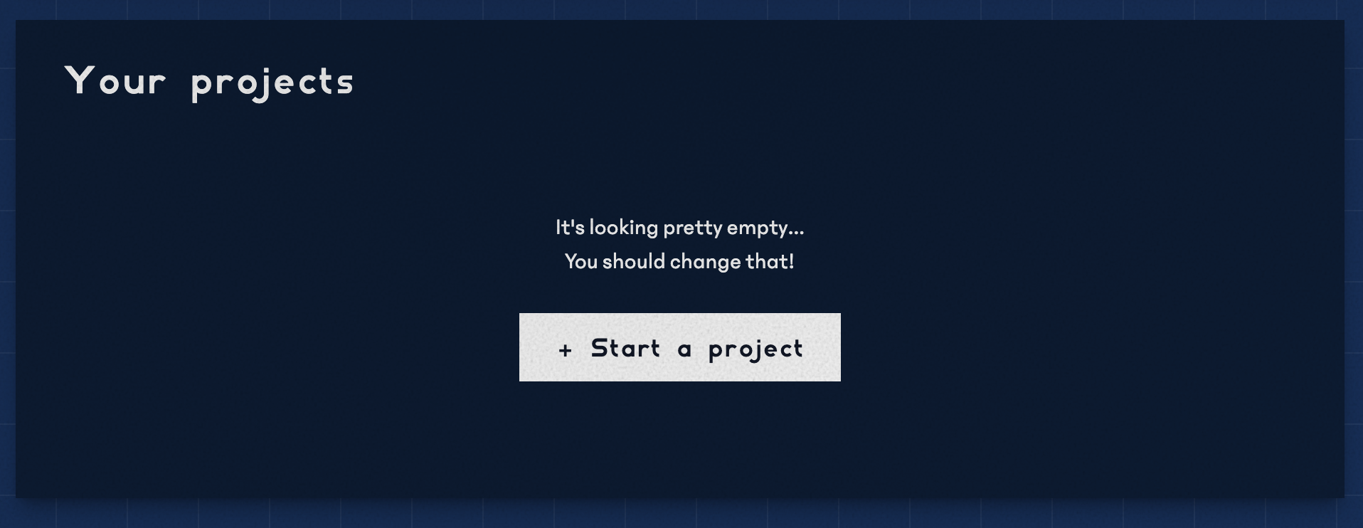
First, head on over to the "dashboard" page and scroll down. You'll see a "my projects" tab! Click "Create new project"
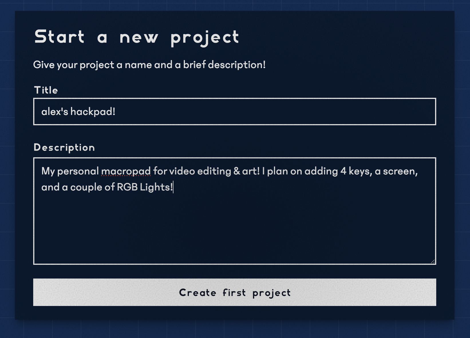
Then, fill in a title + description for your project:
After that, come back here! You're officially done all the setup, so now we can move onto...
Designing your PCB
We're going to be using KiCAD for this part of the guide! Make sure you have it open
To start, we're going to have to install a KiCAD library. We are going to use the following respository:
There are many tutorials on how to install libraries! Google is your best friend here :)
@Cyao in the slack did make an awesome tutorial though! Here it is:
Drawing the Schematic
Start by opening up KiCad, a window will pop up, create a new project then click on the "Schematic Editor" button:

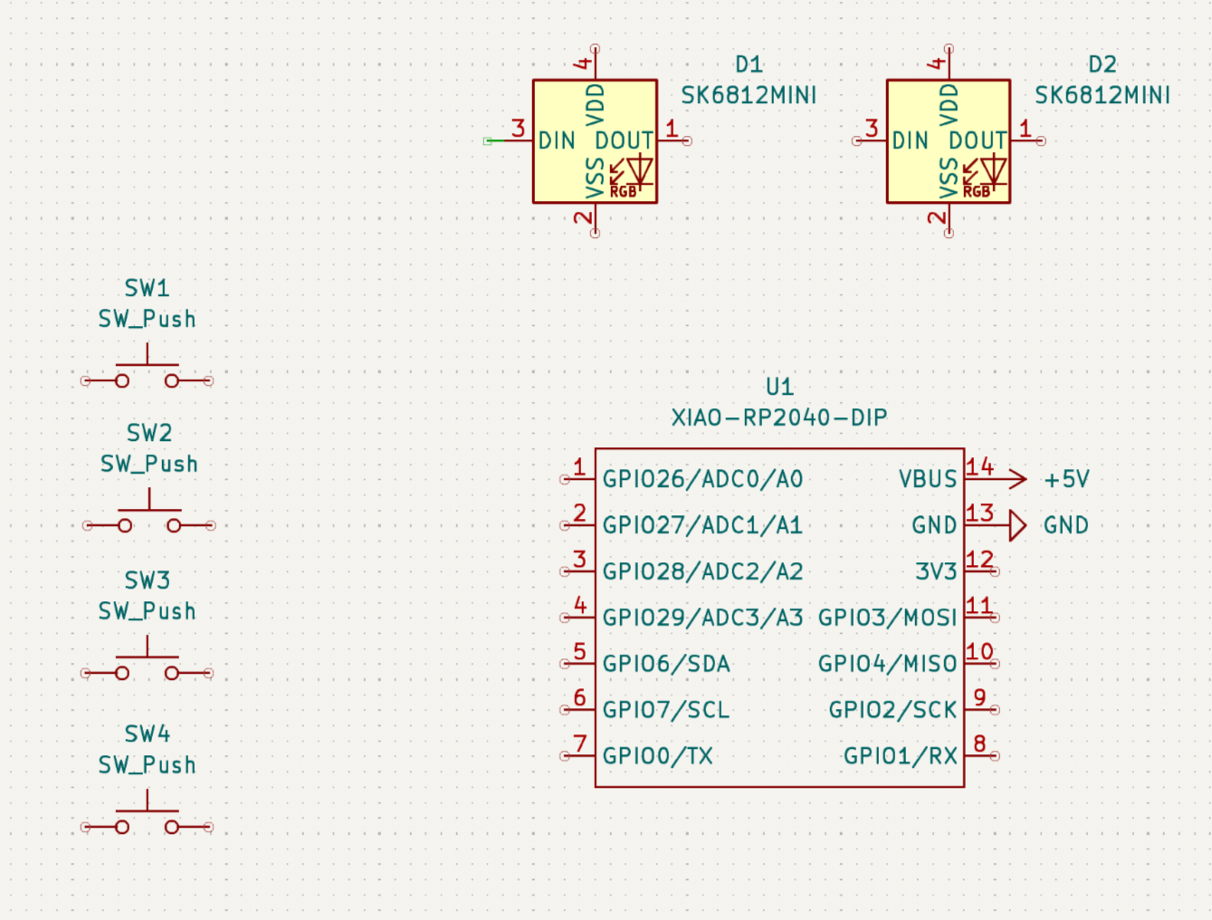
This should open up a new window with your schematic editor! Once you're in, press the A key on your keyboard. This should open up a menu where you can add symbols for your different components! Search for the following to add them:
- XIAO-RP2040-DIP (your microcontroller)
- SW_Push (This will be our keyboard switch! Copy and paste this 4 times)
- SK6812 MINI LED (it's an RGB LED, also known as neopixels - I will be using 2 of these!)
Start by placing these symbols down. They don't have to be in any particular order, but place them somewhat close together.
To rotate the symbols, click R. And to mirror them, click X.
Afterwards, it should look something like this ^^
Now it's time to start wiring. Hit the W key on your keyboard to start wiring! This should make a green wire appear. Connect your components like so:
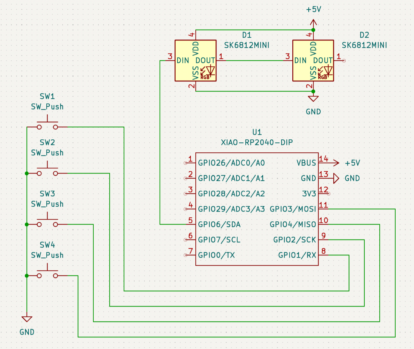
Don't forget to add the GND and +5V symbols! Press P and search for it.
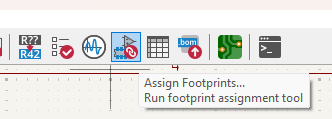
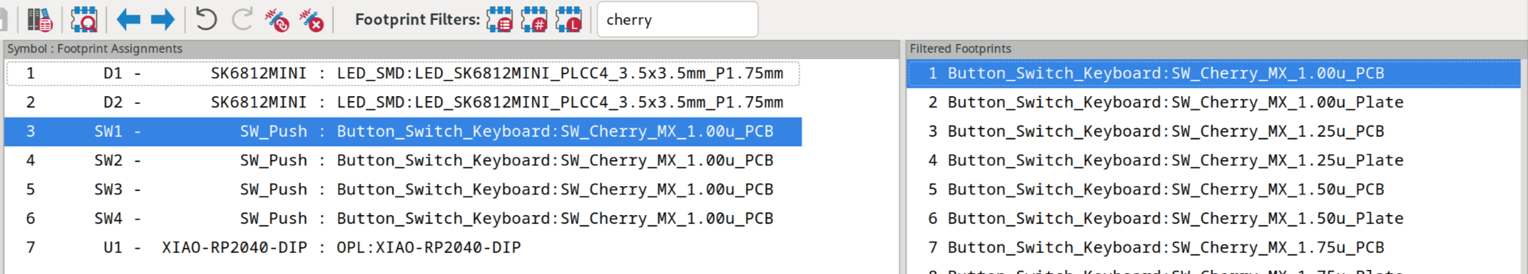
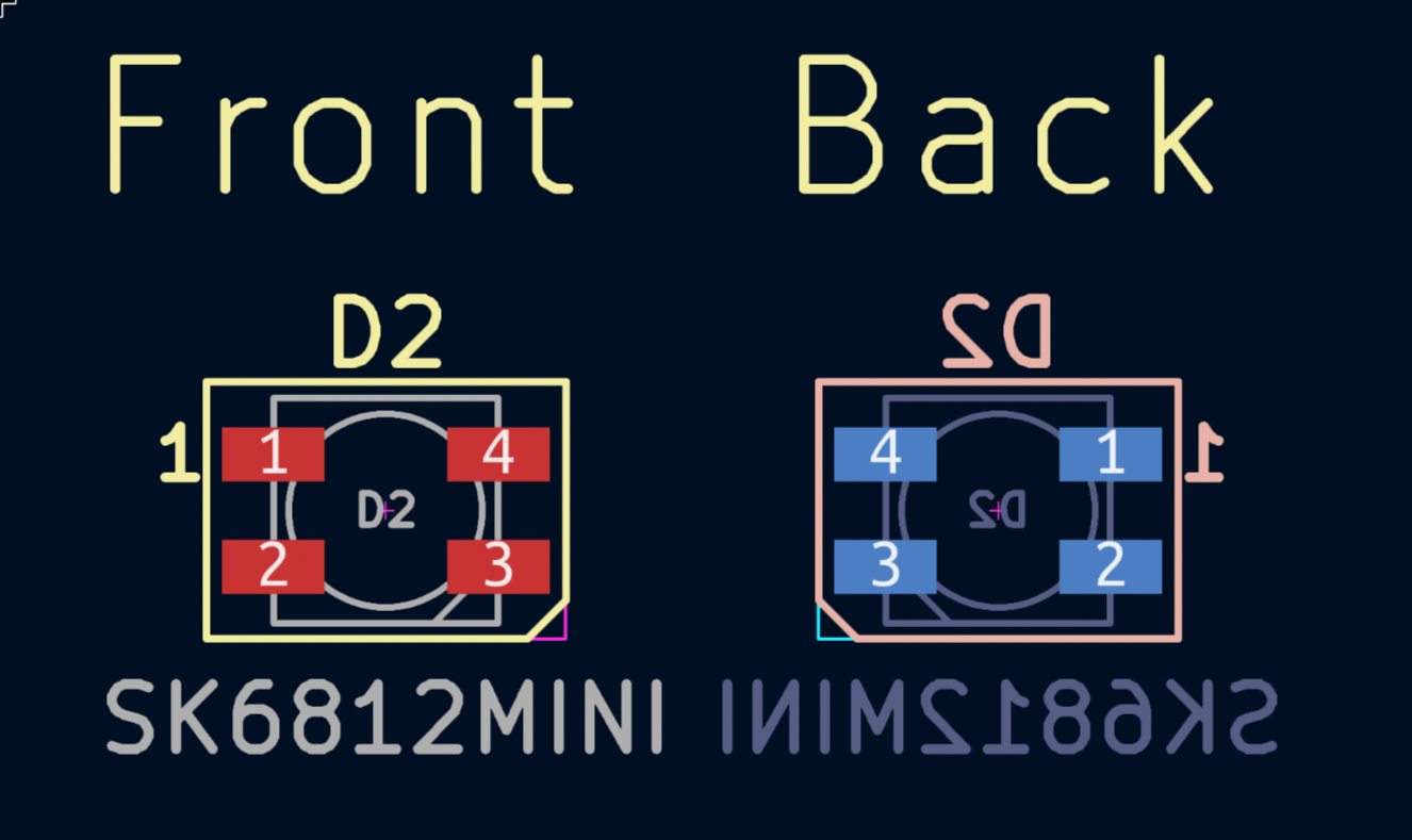
Once all the components are connected, we can start assigning footprints to the symbols we have here. Footprints are what gets physically drawn on the PCB. To do this, click the "run footprint assignment tool" in the top right.
This should open up a window where you can assign different footprints to your components! Assign them based on the image below:
Once you're done, you can hit apply & save schematic. We're now officially done with the schematic! Onto making the pcb itself:
Routing the PCB
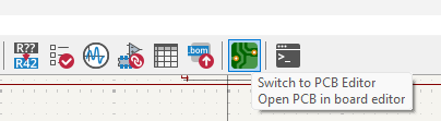
Great job on finishing the schematic! Hit this button to open the PCB editor:
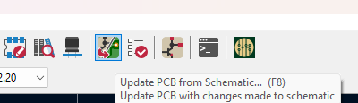
Hit the "Update PCB from schematic" button in the top right. This will bring in all your parts!
Click anywhere on your screen to place your components down, it should look something like this:
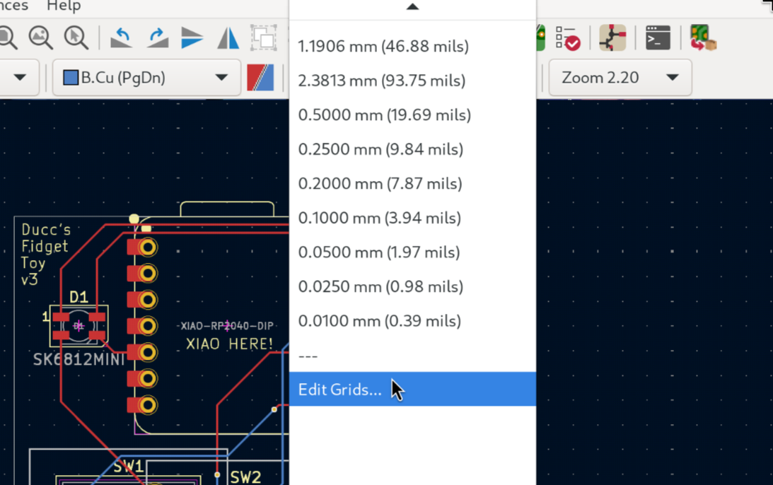
First, to be able to better place the components, we would need to change the grid.
Grids are used to allow efficient placement, movement and connection between symbols and wires. It defines what is the spacing of the grid, which components will snap to.
Select the button at the top that says "1.2700 mm (50 mils)". You can use this menu to change what grid you are on. Then click on Edit Grids...
You should have the following menu open:
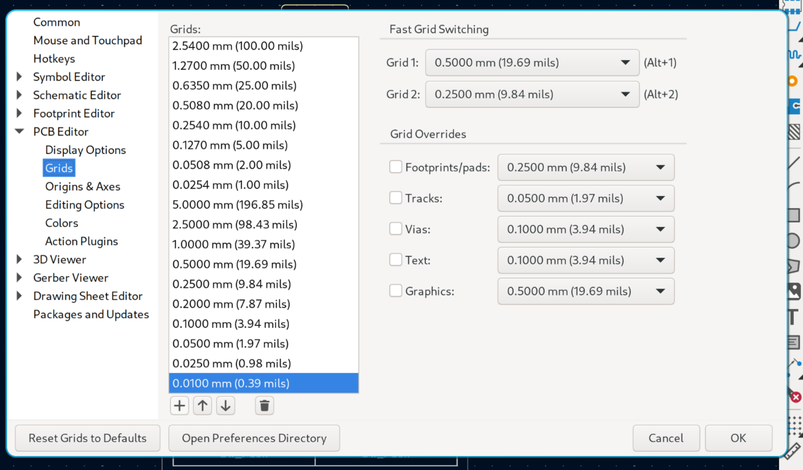
Now click on the + button at the bottom left, and enter "2.38125" in the field named "X". Press Ok, then click on Ok again. Now you have defined a custom grid!
(this is the distance between the switches divided by 8. 19.05mm / 8 = 2.38125mm)
We now need to place the components:
Select a footprint, drag it around to move it (Or if you prefer, click a component to select it, press M to move it and click again to put it down). To rotate the footprint, press R when selecting it.
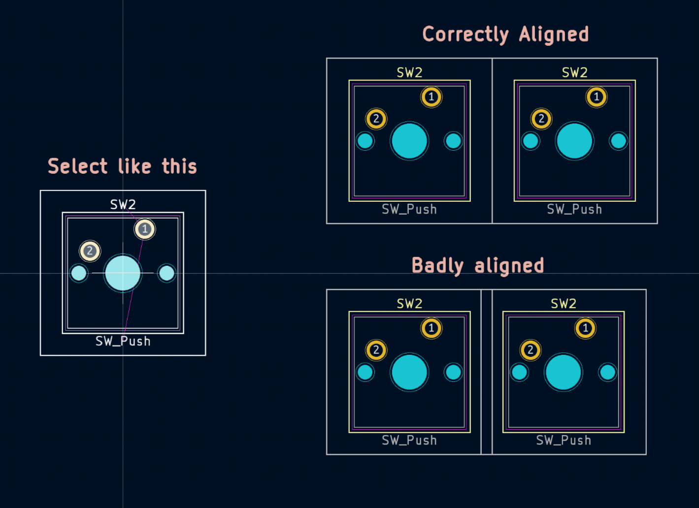
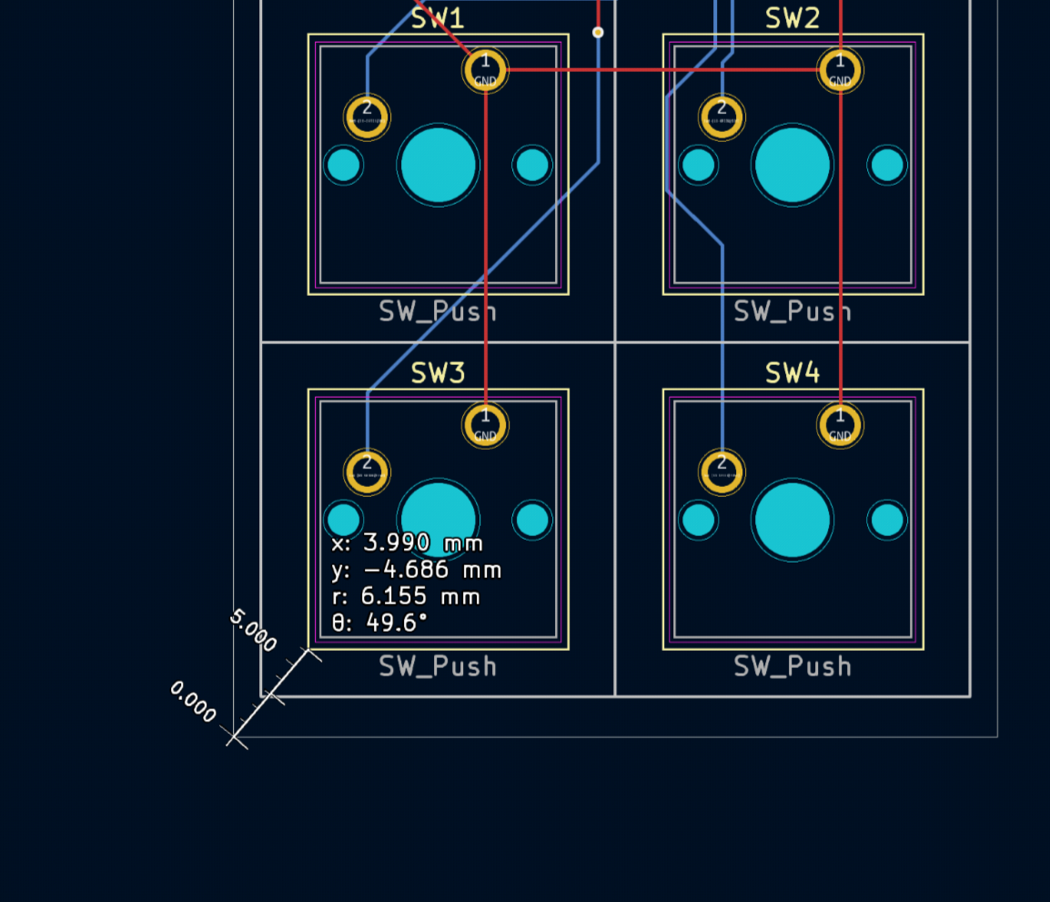
When placing the switches, I recommend you to use the newly defined grid of 2.38125 mm (Select it in the menu), and for placing other components, I recommend a grid of 0.10000 mm. Important: While moving the switches, select the blue circle at the center, this will make sure all the switches are alighed properly. You should align the outer while lines of the switches as so:
There is a front side and back side of the board. You can tell them apart by color
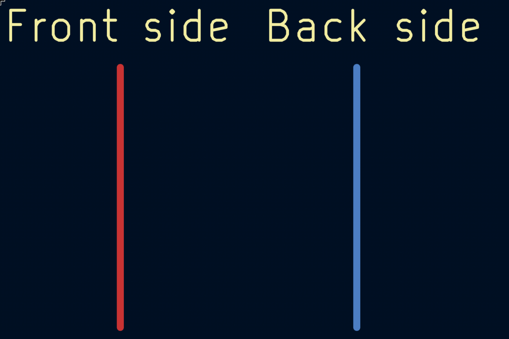
If you want to put the footprint on the back side, press F. Here is what the footprints look like on different sides:
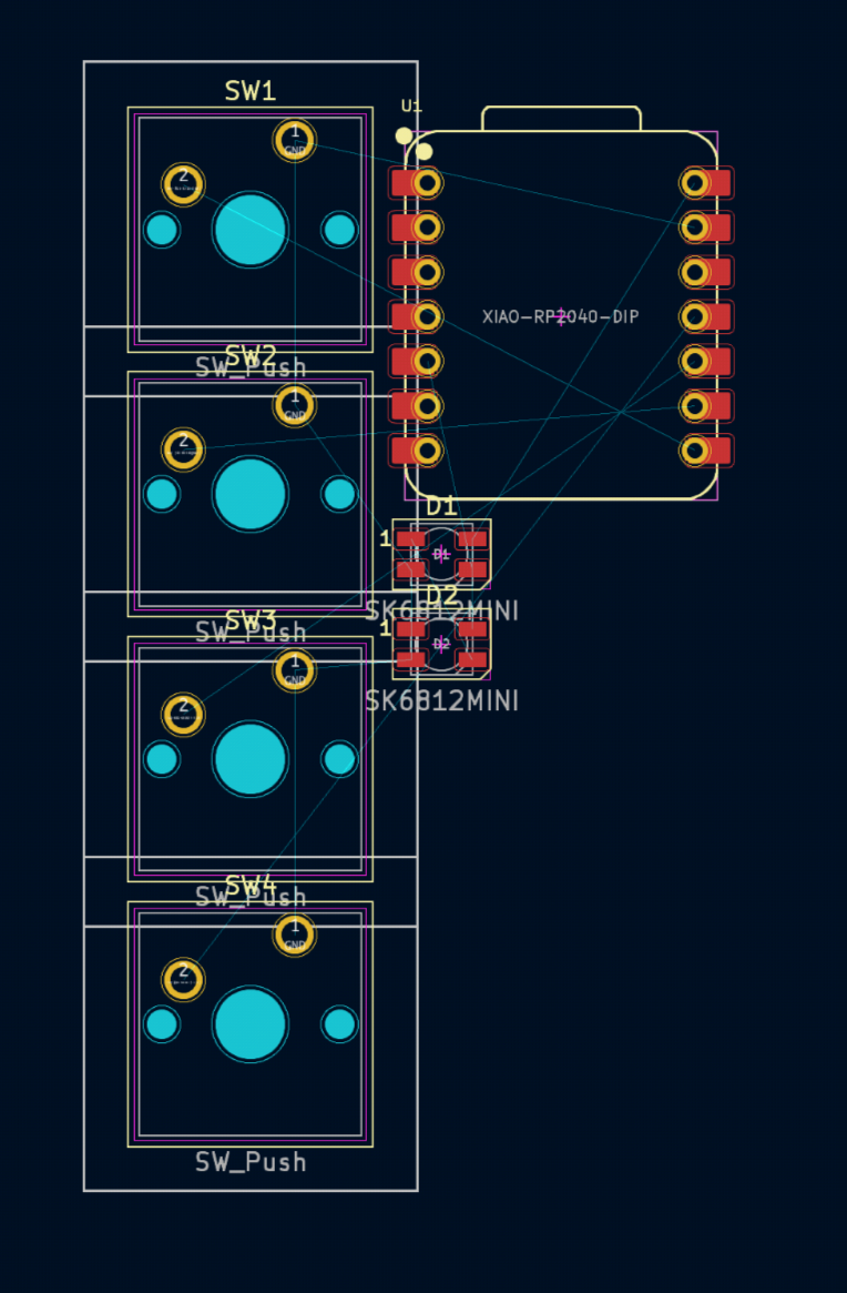
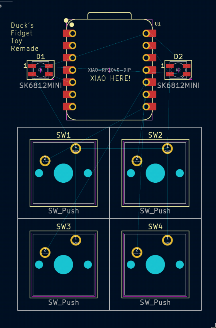
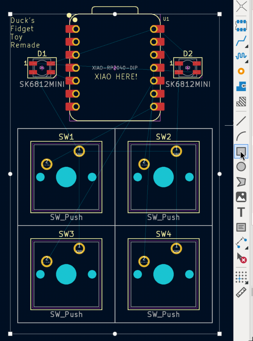
Move, rotate and flip your footprints into a design that you like! It should look something like this:
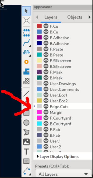
You need to define the outline of the board. Select the Edge.Cuts layer on the right toolbar.
Now, you can use the "Draw Rectangle" button to draw the boarders of the board:
This shall be the size of your physical board.
IMPORTANT! Remember to have the head of the XIAO poking out of the Edge.Cuts rectangle. This is mandatory to be able to plug your USB cable in.
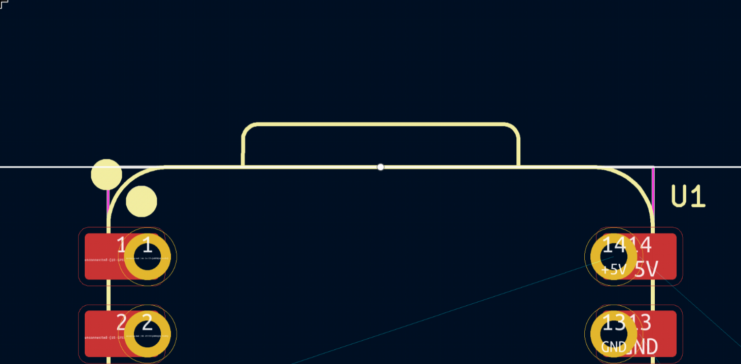
Now it's time to route the PCB! Hit X on your keyboard and hit any golden pad with a thin blue line poking out of it. It should dim the entire screen, show you which direction you need to go with a thin blue line and highlight the destination:
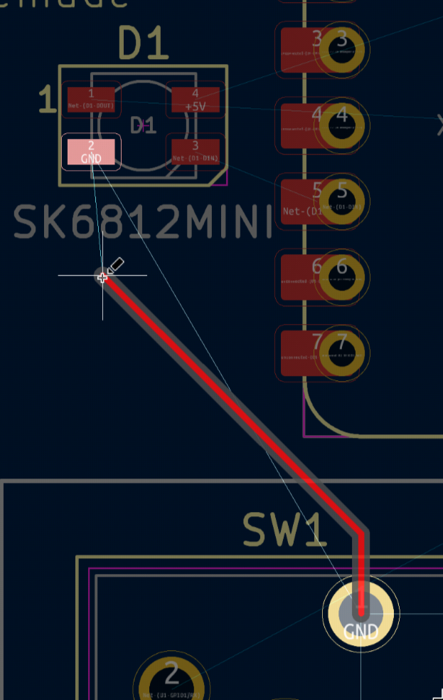
Join the highlighted pads together. If there isn't enough space on the front side, or there is a trace already present that is blocking you, you can route on the back side by clicking B.Cu on the right toolbar. At the same time, if you want to change sides during routing, press V and a via shall be added, which will transfer your trace to the other side of the board:
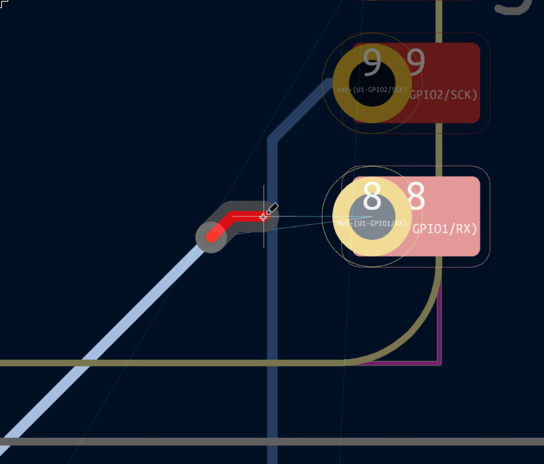
Attention! Wires and pads of different colors (except golden) can't be connected together directly! You must via to the other side.
Continue until there are no thin blue lines on the screen! Your final product should look something like this:
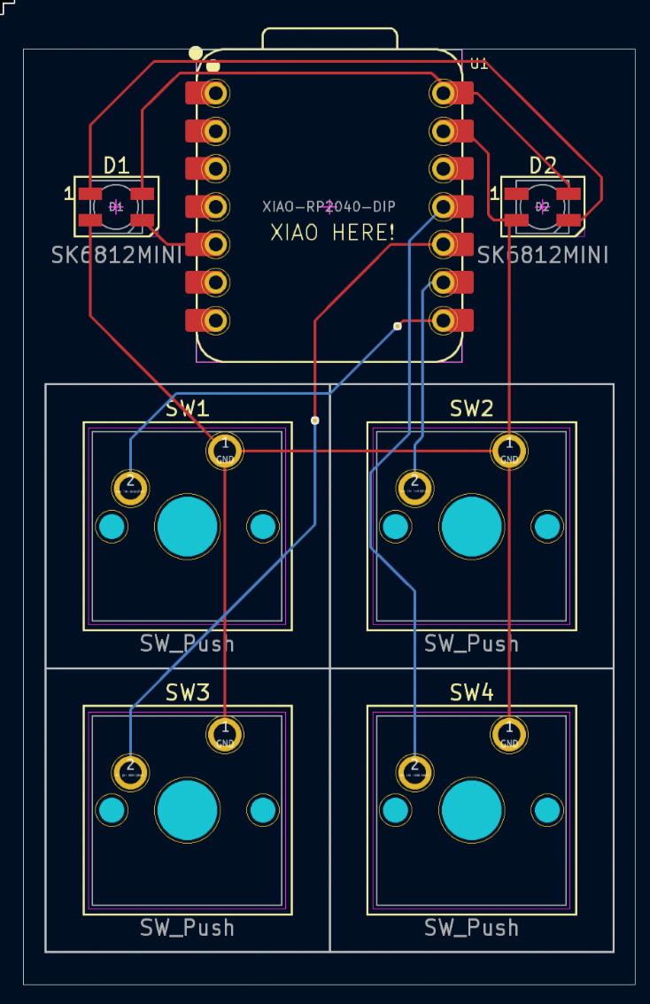
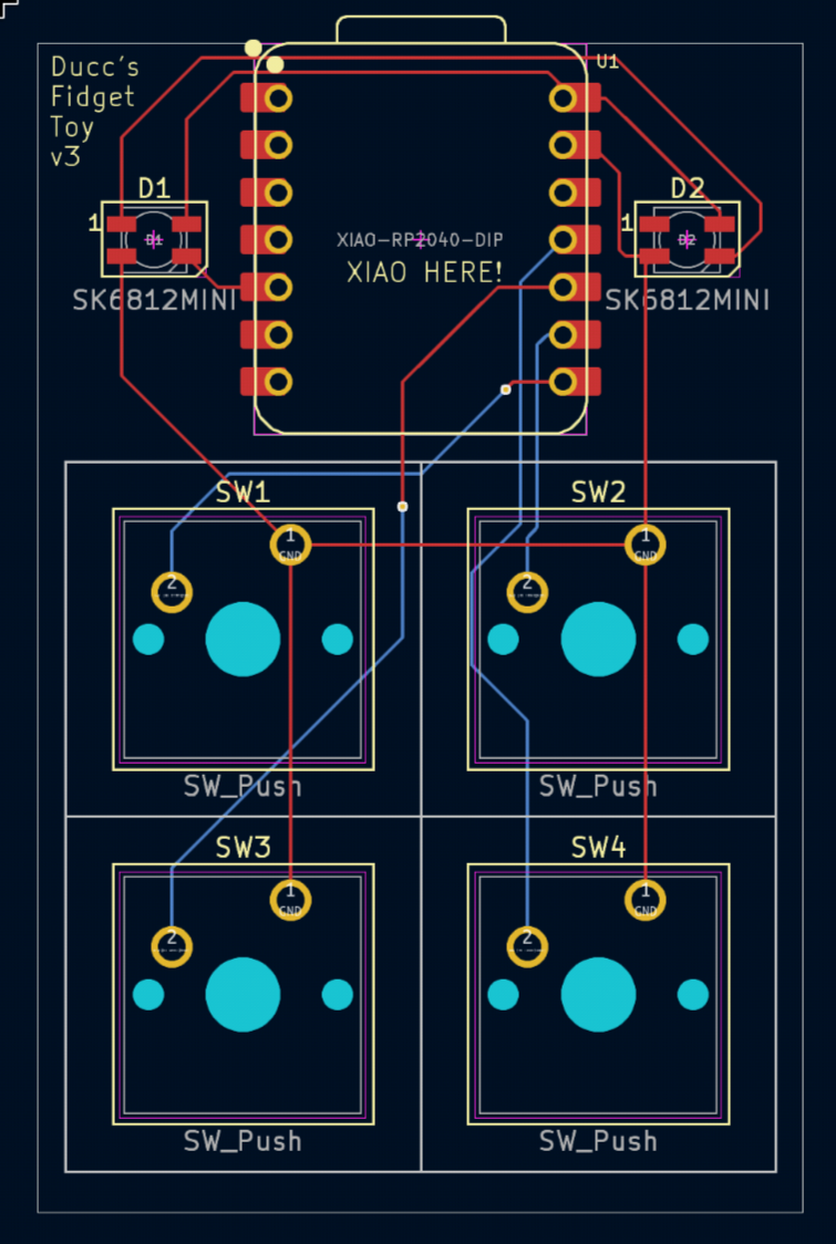
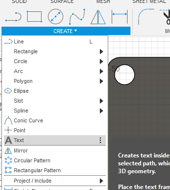
Also, it is VERY IMPORTANT that you brand your hackpad! Put the name of your hackpad on any silkscreen of your PCB. Do this by using the text tool. Also, write "XIAO HERE" on the side you would like your XIAO to be placed on.
To do this select F.Silkscreen (If your xiao is on the back side, use B.Silkscreen when placing the "XIAO HERE" text), and click on the add text button:
Enter your text and place it down!
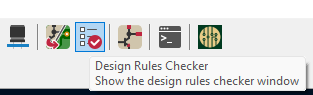
Good work! You're almost done with the PCB. Let's run the DRC to make sure the PCB works. The silkscreen warnings you see are okay, make sure there are no more errors!
PS. You might need to change tabs to see all errors. (Click on "Unconnected Items")
Thats all for your PCB! Great job.
Creating your case
This guide uses Fusion360 for designing the case. You can use other software, but it may be harder to follow along!
First thing first, go to ai03's plate generator.
Then, open keyboard-layout-editor.com in a new tab.
On the top left you should see a small keyboard. Now click the keys that doesn't match your macropad and press "Delete Keys". And if you need more keys, press the "Add keys button". The text displayed on the keys have no importance.
After you made the layout match your macropad, switch to the "Raw Data" tab in the middle:
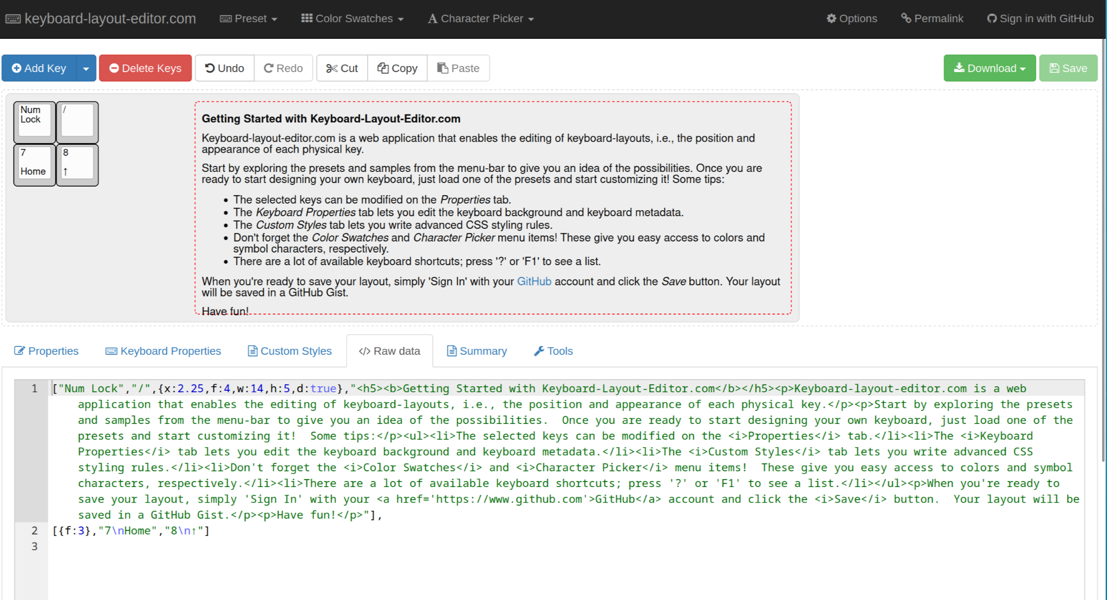
Copy the text inside the textbox, and paste it into ai03's plate generator.
After that, scroll down, look at the preview to verify if it conforms to your macropad, and then press download DXF.
Creating your case in Fusion360
Fusion360 has a free plan for students, you can create a education account. You can also use Autodesk Fusion for personal use After you have your account, either download the native Fusion360 application, or use this magic link to launch it directly in your browser :D
If you are using the browser version, don't forget to save regularly, since your session will close if you leave it alone for too long.
I strongly recommend you use the desktop application if you are on a supported platform, since the web one is buggy and super slow.
Creating the bottom
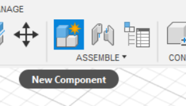
Start by creating a new project, and a new component, this is better for organization.
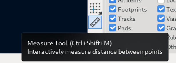
Now go back to KiCAD PCB editor and click on your Edge.Cuts outline. In the bottom left of your screen, you can find the length and widgth of your PCB. Alternatively, measure the dimensions of your board with the ruler tool. Click on one end of your Edge.Cuts and click again on the other end.
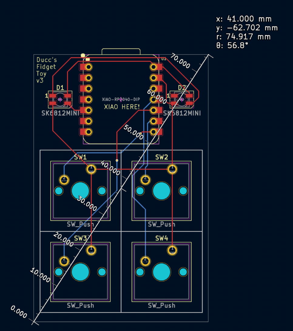
If you used the Edge.Cuts outline, the width and height of your board are the widgth and height listed.
If you used the ruler tool, the width of the board is the absolute value of x (41mm in my case), and the height is the absolute value of y (62.702mm) in my case.
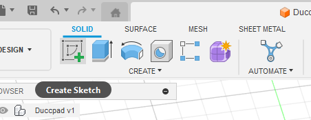
Next, create a sketch by by pressing the green + button on the top left, then clicking the bottom orange retangle at the center of the screen.
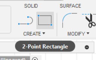
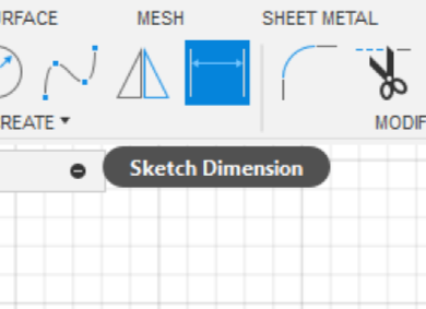
Create a rectangle that is 1mm bigger than your hackpad's PCB. For example, my PCB is 41mm x 62.7mm, I added 1mm to each size on the sketch. To set the size of a rectangle, click on the Sketch dimension button (You might need to expand the "Create" menu to see it, or press the D key), then click on the edge you want to define the length.
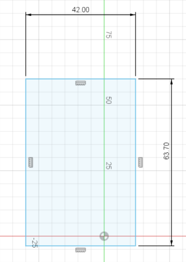
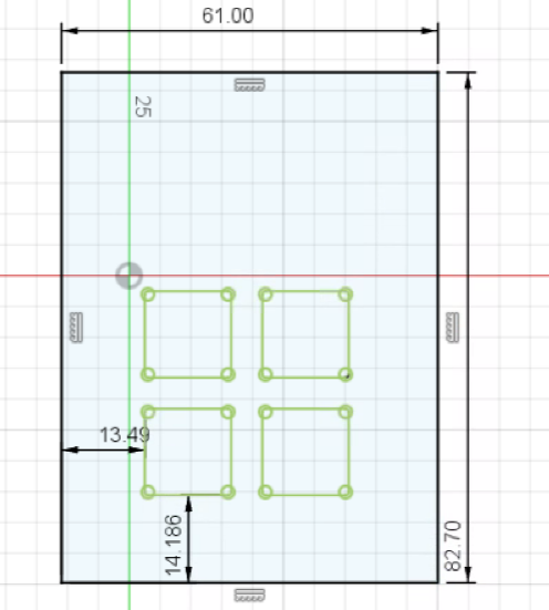
Create another rectangle with 20mm extra on each dimension! (I will have 61mm x 82.7mm):
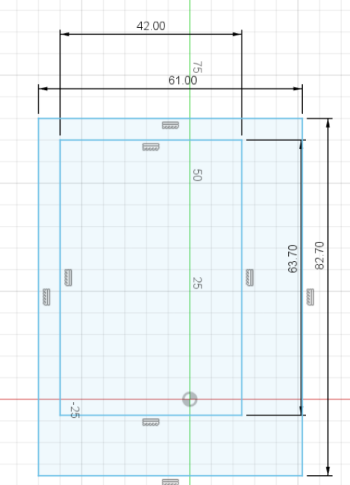
Center this rectangle by pressing the Sketch Dimension button, press one edge of the small rectangle then the corresponding edge of the big rectangle and setting the values to 9.5mm. (You only need to constrain one of the horizontal edges, and one of the vertical edges)
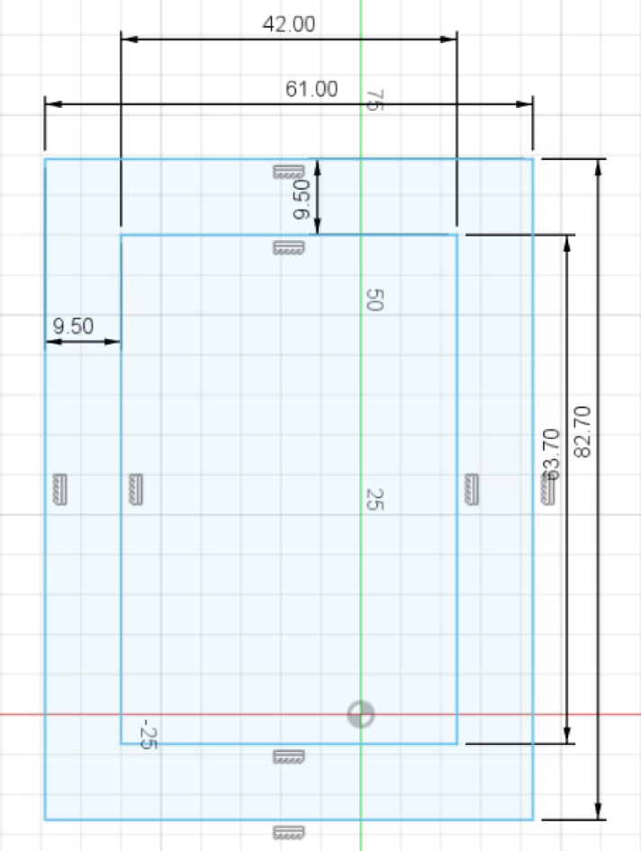
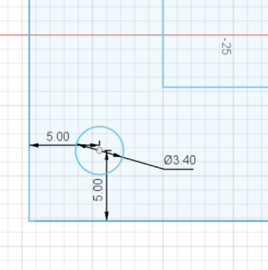
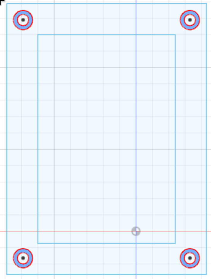
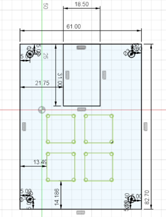
Now use the circle tool to draw 4 circles, one at each corner of the larger rectangle. Set the diameter to 3.4mm when creating the circle, or use the sketch dimension tool to set their size to 3.4mm. Then, use the dimension tool to set their distance to their corresponding edges to 5mm (by clicking on their centers, then the corresponding edge):
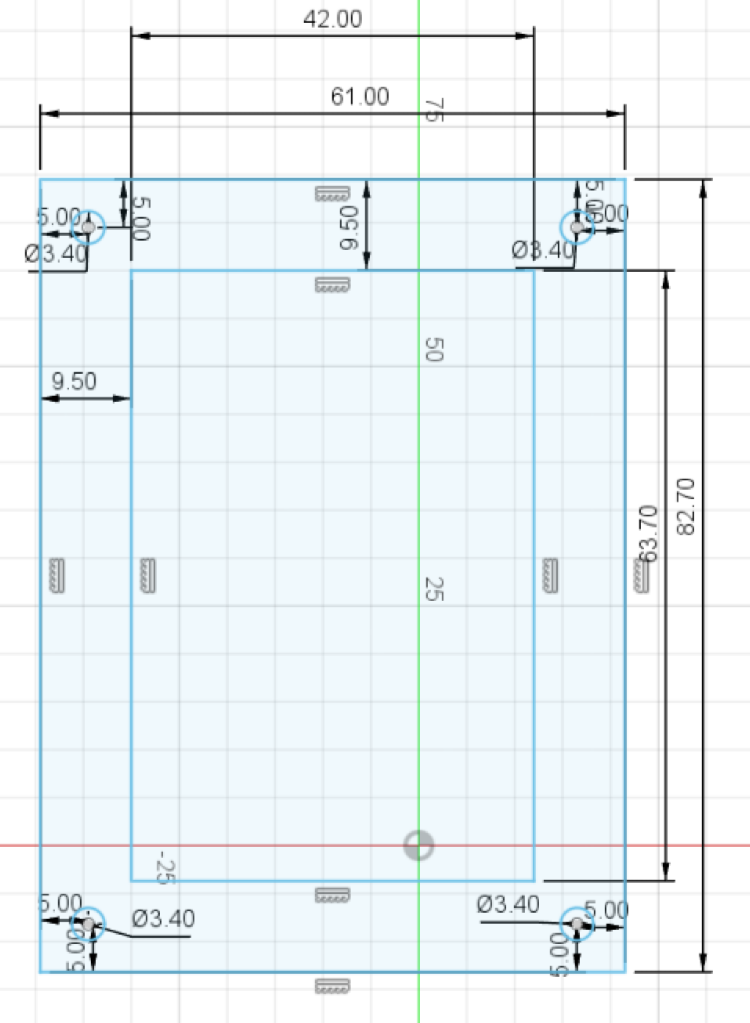
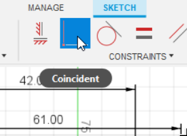
Now add 4 more circles, this time with a diameter of 6mm. Select the center of the small circle when you place the larger circle's center point, or select the coincident tool, and click on the centers of corresponding circles to align them.
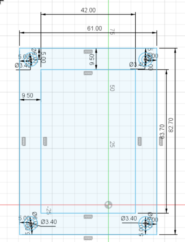
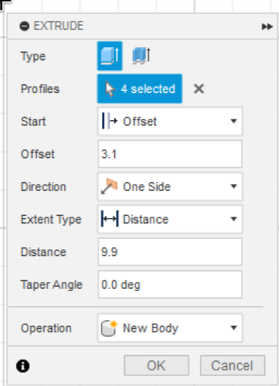
Press "Finish sketch" (green checkmark at top right of screen), then select all the outer circles (shift click) and press extrude (E key or the button at the top). In the extrude menu, select Offset in Start, and enter 3.1mm as the Offset, then enter 9.9 mm in the Distance field and click ok:
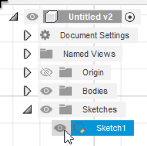
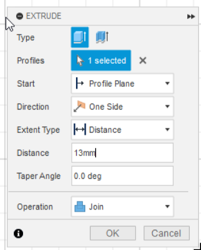
Now, you must re-show the object be opening the Sketches folder on the left, and clicking the eye icon to the left of Sketch1. Then select the outer rectangle and press extrude. This time the Start shall be "Profile Plane" (and will be this for all future extrudes), and set the distance to 13mm:
Now, click the center square, and extrude it by 3mm. You can move arround and you will see something like this:
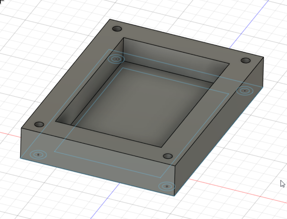
That's the base of your case done!
Now go to kicad and measure the distance from the edge of the PCB to the USB port using the ruler tool
Now select the top of the case:
And create a new sketch (Create Sketch button). Draw a rectangle at the top, and place your starting point on the top edge, and ending point on the inner top edge. Now define it's width to 18.5mm (You can define it by clicking on the left edge, then the right edge with the distance tool). After that, set the distance from the left of the rectangle to the left edge of the case to xdistancein_kicad+5.75mm:
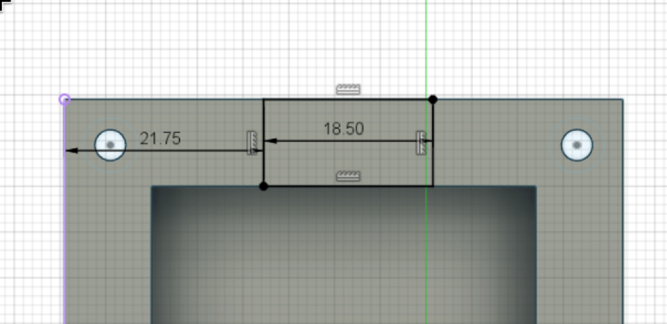
Click finish sketch, select the rectangle we just drew and press extrude. This time set the distance to -7.5mm
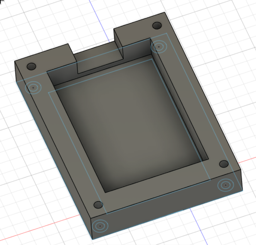
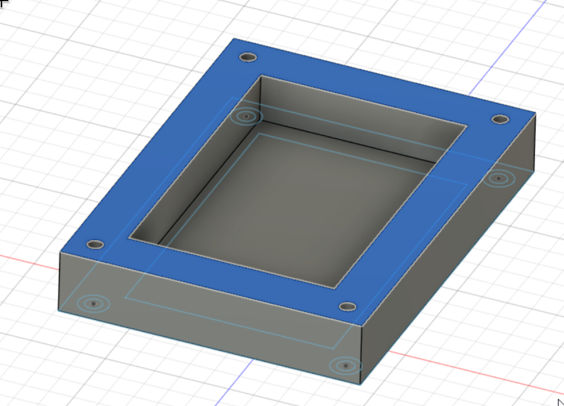
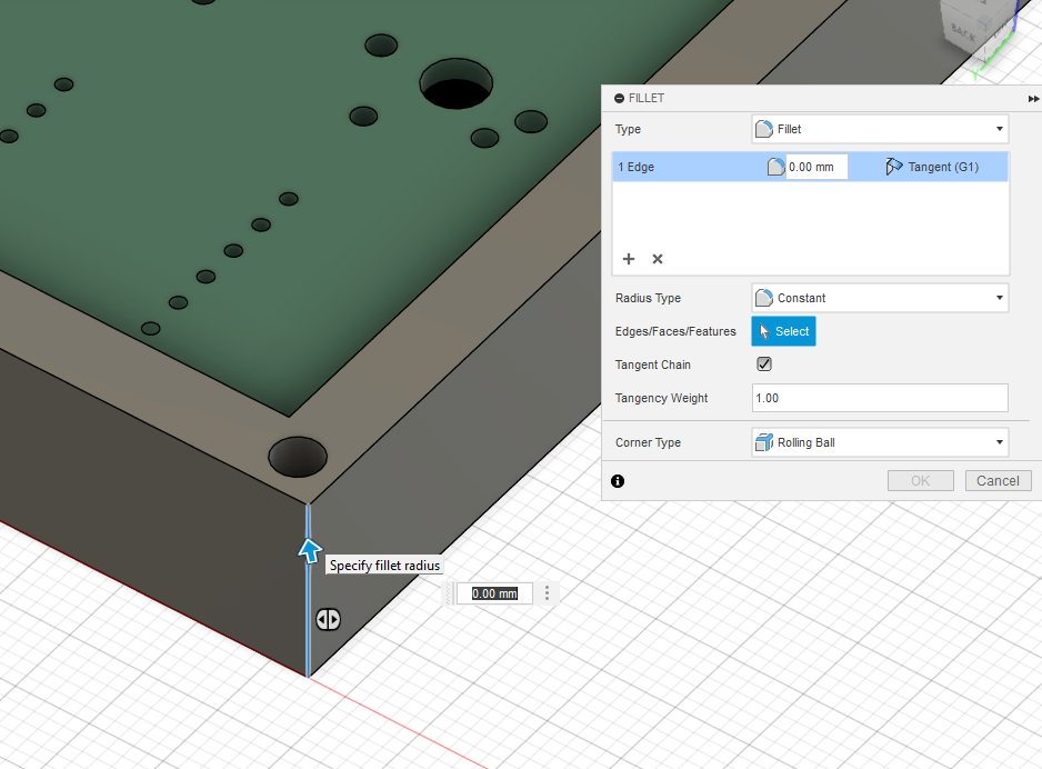
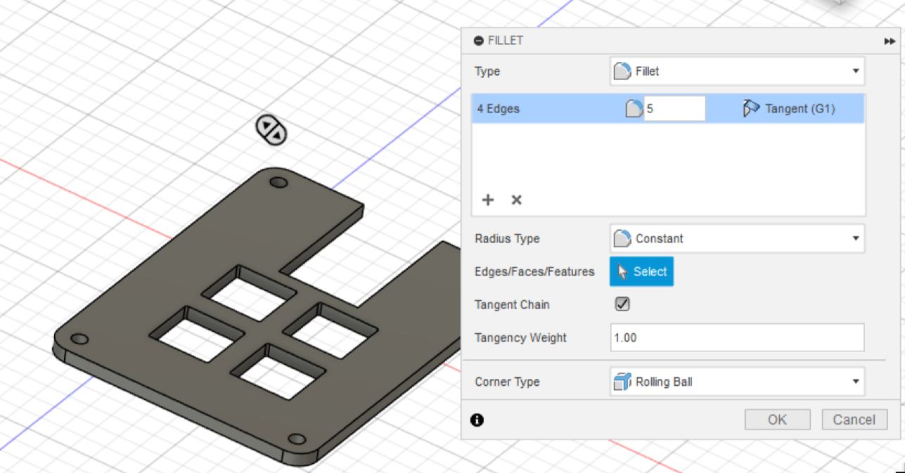
Right now our case looks a little ugly, it's so blocky! Lets round the vertical edges, press the Fillet button found in the top, click on each edge and make it 5mm. Should look as such:
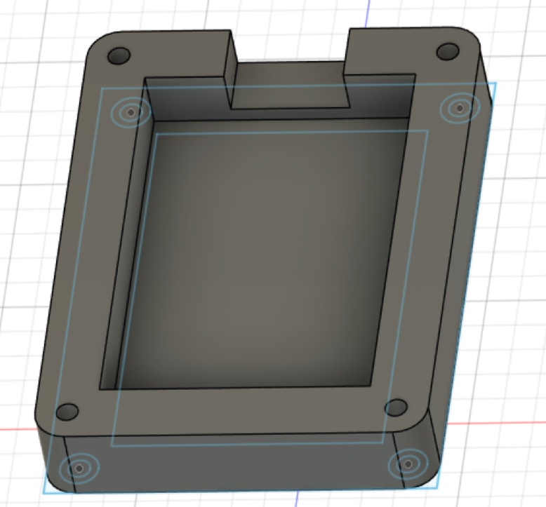
Now we finished the bottom case! Congratulations!
You can now export the model by clicking File > Export... at the top left, and selecting STEP Files as the Type.
To download the resulting STEP file on the web, go to https://myhub.autodesk360.com/, go to your project and click the download icon.
Creating the top
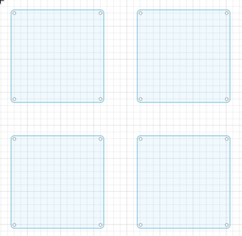
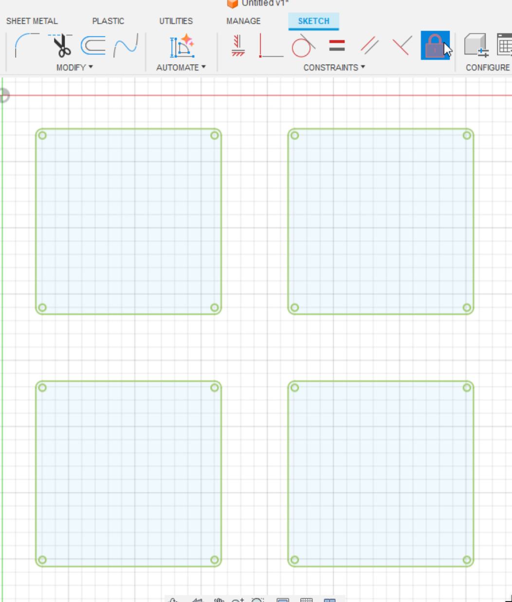
Next, we will make the other half of our case. Start by clicking new design.
Now go to the INSERT menu, expand it and click "Insert DXF". Select the dxf file we generated at the start (in the web you need to first click Upload from Fusion Team..., upload it from there, click refresh then select the file), and click ok. Now delete the outer lines surrounding the keyholes. You should have something like this:
Now select everything and click on the Lock button
Go back to KiCAD PCB editor and measure the dimensions of your board with the ruler tool. Click on one end of your Edge.Cuts and click again on the other end. You can also select your Edge.Cuts and find the width and height in the bottom right.
Now lets create a new rectangle, define it's width and height be the same as the size of the top plate. Set the distance between the left keyhole end and the left rectangle edge the x distance you just measured + 9.5 (for me it's 3.99+9.5). Same for the bottom edge of the keyhole and bottom edge of the rectangle, y distance + 9.5.
Add another rectangle, this time with it's start starting on the top line of our rectangle. Set it's width to 18.5mm and height to 31mm. After that use the distance tool to set the distance from the left of the innder rectangle to the left edge of the outer rectangle to xdistancein_kicad+5.75mm
Add 4 more circles of 3.4mm and set their position to 5mm from the edges with the distance tool:
Click finish sketch, and pad out the main part by 1.5mm.

But currently the plate is kinda ugly. Do the same things with the fillet as the case:
You finished your plate!! Congrats 🎉
Finishing Touches
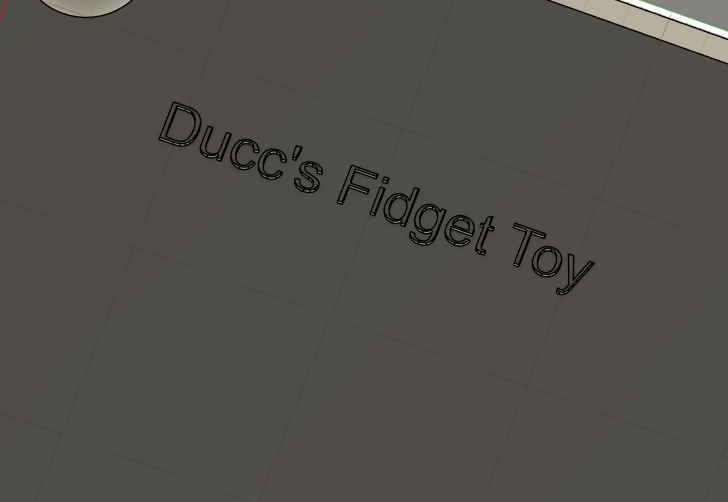
Next, we will brand our case! This part will not be seen and is for us to be able to keep track of who's submission is whos. Go to the bottom of the case, or somewhere that won't be seen, and create a new sketch. Make a text box, and enter the name of your hackpad on it.
Extrude this sketch 0.2mm INTO the case, don't worry about the overhang! If you are getting an error when extruding, keep the font as Arial.
Thats it! Your case is now done.
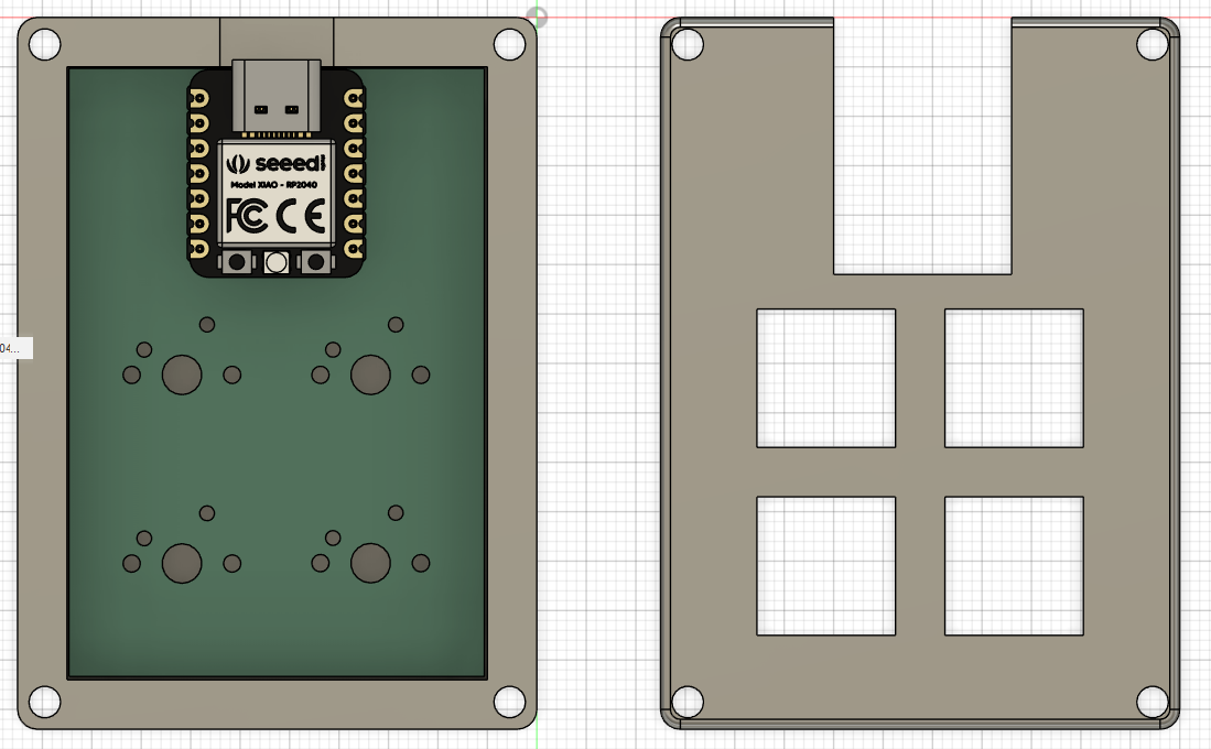
I would also recommend importing 3d models of all your components to test fit everything:
Firmware
You can use the QMK firmware project as firmware! You can find out how to port your keyboard here: \
QMK Porting Guide
Or if you wish, you can use kmk. It's made in python and can be hot reloaded.
Here is the starter code, with explanations in the comments:
# You import all the IOs of your board
import board

# These are imports from the kmk library
from kmk.kmk_keyboard import KMKKeyboard
from kmk.scanners.keypad import KeysScanner
from kmk.keys import KC
from kmk.modules.macros import Press, Release, Tap, Macros

# This is the main instance of your keyboard
keyboard = KMKKeyboard()

# Add the macro extension
macros = Macros()
keyboard.modules.append(macros)

# Define your pins here!
PINS = [board.D3, board.D4, board.D2, board.D1]

# Tell kmk we are not using a key matrix
keyboard.matrix = KeysScanner(
    pins=PINS,
    value_when_pressed=False,
)

# Here you define the buttons corresponding to the pins
# Look here for keycodes: https://github.com/KMKfw/kmk_firmware/blob/main/docs/en/keycodes.md
# And here for macros: https://github.com/KMKfw/kmk_firmware/blob/main/docs/en/macros.md
keyboard.keymap = [
    [KC.A, KC.DELETE, KC.MACRO("Hello world!"), KC.Macro(Press(KC.LCMD), Tap(KC.S), Release(KC.LCMD)),]
]

# Start kmk!
if __name__ == '__main__':
    keyboard.go()
If you have something more advanced on your PCB, look inside the kmk docs for how to add it!
Save it in a main.py file in the firmware folder of your repo
Now after you received you macropad, plug it in and hold the bootloader button and press reset. You should see a external drive on your PC, download circuitpython and drag the file onto the drive.
The board should automatically restart and be recognised as a new external drive. Now download kmk, unzip it and copy the KMK folder and the boot.py file to the root of the external drive. Then create copy your main.py file over. And voila you got your macropad!
Next steps
We just made a pretty cool macropad, but obviously there's a lot of cooler stuff out there - that's up to you to figure out! Again, don't copy this guide 1:1, add your own design into it.
Want some resources and tips? Check this out!
Or maybe do you think you are done? Check out how to submit here