AngstromIO, a devboard the size of a USB-C connector (+ the programmer, & another CH32v003 devboard)
AngstromIO is one of the smallest devboards out there, barely longer than a USB-C connector, based on the ATtiny1616 MCU (16kB flash). It comes with 2 Addressable RGB LEDs, and 2 GPIOs as well as I2C lines are broken out. I made a dual CH340 programming board too, both for UPDI programming and debugging (one way Serial Communication). The third PCB is a cost effective, USB-C devboard based on the CH32v003 (QFN) with a small 5x4 charlieplexed LED matrix.
Created by
 Clém
Clém
Tier 4
1673 views
8 followers
 cubit010 ⚡
approved AngstromIO, a devboard the size of a USB-C connector (+ the programmer, & another CH32v003 devboard) ago
cubit010 ⚡
approved AngstromIO, a devboard the size of a USB-C connector (+ the programmer, & another CH32v003 devboard) ago
Tickets awarded: 281 tickets
Tier: 3
this is amazing and very well polished
good work!
 chris
gave kudos to AngstromIO, a devboard the size of a USB-C connector (+ the programmer, & another CH32v003 devboard) ago
chris
gave kudos to AngstromIO, a devboard the size of a USB-C connector (+ the programmer, & another CH32v003 devboard) ago
https://www.cnx-software.com/2026/03/26/angstromio-a-tiny-9-0-x-8-9-mm-attiny1616-board-that-fits-on-top-of-a-usb-c-connector/ Found something
Clém
submitted AngstromIO, a devboard the size of a USB-C connector (+ the programmer, & another CH32v003 devboard) for ship review ago
 CAN ⚡🚀
approved AngstromIO, a devboard the size of a USB-C connector (+ the programmer, & another CH32v003 devboard) ago
CAN ⚡🚀
approved AngstromIO, a devboard the size of a USB-C connector (+ the programmer, & another CH32v003 devboard) ago
Tier approved: 4
Grant approved: $0.00
Awesome project!
Clém
submitted AngstromIO, a devboard the size of a USB-C connector (+ the programmer, & another CH32v003 devboard) for ship review ago
Clém
added to the journal ago
Assembling the CH32 devboard
I assembled one CH32 devboard, and adding the solder paste on all the pads was a tedious task, since I don't have any stencil. I think that for bigger LED matrices, I'll definitely buy a stencil. Anyway. I then placed all the components, making sure the 20 0402 LEDs were in the right orientation, and after reflow soldering the board, I tested it with the custom firmware right away: And I was really happy to see that everything worked first try! Even the Charlieplexed LED matrix! yay! ... when trying to hook the WCH Link-E to the devboard, I just noticed that I didn't had the TX UART pin broken out (I used it for the LED matrix), so I won't be able to get any Serial communication.
I then soldered pin headers (yeah, I know, the solder joins aren't perfect, especially for the PWR pins, but I forgot to add thermal reliefs, so it was kinda hard to get the solder to melt...)...
Anyway:
The board was ready for a small photoshoot...
Gallery
.jpg)
.jpg)
.jpg)
.jpg)
.jpg)
.jpg)
.jpg)
.jpg)
.jpg)
.jpg)
Small game: Can you spot the differences? 😂
.jpg)

Clém
added to the journal ago
Coding the CH32 devboard demo
I coded the Demo code for CH32 devboard, which mainly consisted of handling the 5x4 charlieplexed LED matrix. I took a few functions from my IOX-77 project for the CH32, this way I could just focus on handling the matrix with the pinMode(), digitalWrite() and digitalRead() functions. Developing the code for the charlieplexed matrix was kinda mind-bending, but thanks to bitluni's explanation, I was able to create the required code for my 5x4 LED matrix... or at least I think it'll work as expected...
So basically, I've got a set of arrays, some containing the different LEDs configurations (like digits from 0 to 9), or an all-white and all-black array), which are used by the function updateDisplay() to display the image. it scans the display columns by columns (setting the corresponding column to LOW), and each row is driven simultaneously (HIGH or HI-Z)in accordance with the array in parameter. Each column is updated every DELAY_FRAME milliseconds, 2ms here, and the process is repeated over and over the number of times required to last duration ms.
I've created a small demo which uses all the features of this devboard: The orange LED on PC0 blinks until the button (PD0) is pressed, and then a countdown from 9 to 0 starts, ticking down every 1s. It then blinks the digit 0 two times before lighting all the LEDs up, to ensure they are all working correctly.

Clém
added to the journal ago
Assembling the AngstromIO and programmer
I finally received the PCB and components, and just realized how tiny they were... I mean, I knew the mini devboard would be smaller than 1cm², but it always looks bigger on the design on the screen, so... Anyway that is so cool!


I started assembling 2 AIO on one panel, carefully adding small blobs of solder paste with the seringe onto each pad (I didn't bought a stencil), and I add to make a few retouches with some tweezers and a small bit of tissue to remove the excess paste on some pads. I checked multiple times with my phone, realizing that with a 8x zoom, it can give pretty good results, a bit like a digital microscope, or at least it's still better than looking to the naked eye. Once I was satisfied, I populated 2 devboards, checking on the design files the orientation of the 1.5 by 1.5mm addressable LEDs (one of the two is rotated 90°) and added the few components on the top side (MCU (QFN20), resistors and capacitors (0402))

I then reflow soldered the boards on my hot plate, and had to use the tip of my soldering iron to remove the few solder bridges on the QFN IC. I really wanted to test the board before soldering the USB C on the other side, so... I assembled the programmer too. This time I snapped it directly from the panel, but other than that, it was the same process that followed: adding solder paste, placing the components while checking the orientation of the 0402 LEDs, reflow solder the boards, and retouch the solder bridges on the ICs (I had to remove one CH340 IC before putting it back on the PCB to get rid of the solder bridge on the D+ and D-, but it turned out easier that I thought, considering the legs on the MSOP-10 are quite long and close to each other).
I plugged the programmer on the computer, and it was recognized on the computer. Nice. After detaching the boards from the panel and sanding down the mouse bites, I then soldered thin-yet-bulky-compared-to-the-AIO cables to the mini devboard, on VBUS, GND and UPDI to try it right away, and uploaded the Arduino demo sketch on the AIO, and was really happy to see that it worked well, lighting up the 2 LEDs, meaning that the soldering process went really smoothly. Hurray!
.jpg)
.jpg)
.jpg)
Now that the top side is correctly soldered, I dealt with the other side, that while only having 3 discrete components, still scared me a bit because heating the bottom side up with the air gun could, and turned out it happened with an LED, make the components fall from the other side so I had to resolder it after (that's why double sided assembled PCB is usually done with two different solder paste, one with a higher temp that the other...)
Eventually I got the 2 AIO soldered, and finished the build by hand soldering the 4 legs USB-C, and that's where you understand why JLCPCB provides a 'Castellated holes' option, since the castellated holes made with the default process didn't turned out great... There were bits of copper everywhere in the hole but on the edges, but I still managed to solder the USB-C properly, even though the solder joins looked a bit weird with the tin sticking to the excess copper bits.
On one AIO, I ended up connecting wires on all the tightly packed solder pads, making it kinda breadboard friendly while completely defeating the purpose of having a small devboard, but I don't care since I'll certainly use this setup for prototyping with the ATtiny1616, so it's easier with the pins accessible. I kept the second AIO without any soldered wires, because it'll be used that way, and once the board is powered via the USB-C, it will be possible to program it directly by pressing a jumper wire to the UPDI pin, without any soldered programming wires... As long as there are common grounds, i.e. the devboard is connected via USB to the same device (laptop or power source) that the programmer.
.jpg)
... Actually you may remember that for the programmer to be powered, the 'Serial' (UART) side has to be connected to the PC, since it's the only USB-C providing power, so it means that with the AngstromIO connected too, I'll need 3 available USB ports on the host (the computer) for programming... So I might need to use a USB hub for my laptop...
And, that's official, I've measured the AIO dimensions. It's indeed 9mm long, but for the width, it's more 9.5 (instead of the 8.9) advertised, but it's just the solder join being too thick. I think that with the other boards I should be able to obtain the 9mm wide, using solder paste intead of manually soldering the 4 USB C legs.
.jpg)
.jpg)
Anyway that's enough talking, I'll let you appreciate this cute lil devboard, laying down on my index...

Gallery:
.jpg)
.jpg)
.jpg)
.jpg)
.jpg)
.jpg)

.jpg)
.jpg)
.jpg)
.jpg)
.jpg)
 kanokid
gave kudos to AngstromIO, a devboard the size of a USB-C connector (+ the programmer, & another CH32v003 devboard) ago
kanokid
gave kudos to AngstromIO, a devboard the size of a USB-C connector (+ the programmer, & another CH32v003 devboard) ago
This looks awesome! I like the way you paneled and how tiny you could make the AngstromIO.
Clém
added to the journal ago
AngstromIO demo code
I just needed a small demo code, that I could run on the AIO as soon as the boards are soldered, but the advantage of being Arduino compatible (thanks to megaTinyCore), is that with the right libraries, the code is really easy. So I made a quick demo code using the tinyNeoPixel.h library (the Neopixel library adapted for megaTinyCore).
The code is pretty straightforward, it simply test the Serial Communication and run a custom function, which lit the 2 RGB LEDs with different colors. obviously (and I'm mentally prepared for what is coming...), the CH32V003 devboard code difficulty will be on another level...

Clém
added to the journal ago
The Pinout:
Any development board, most importantly than any other electronic breakout board, requires a pinout documentation. So I made a documentation for the AngstromIO, CH32 devboard and UPDI/Serial Programmer, explaining the functions (and alternate functions) of each pin, as well as some comments on what each components does:


Clém
added to the journal ago
Rendering the programmer and CH32 devboard
I did the same thing for the programmer and CH32 devboard, exporting from EasyEDA, manually adding the few missing components (USB C, 0603 caps, SOT23, and the 2 CH340), adding the tinned pads, changing the appearance...
For the CH32 devboard, I also added the header pins, breadboard and USB C cable, because this board is meant for prototyping on a breadboard.
And once again, I let Fusion 360 cook my CPU at 96°C...
Seeing it thermal throttle at 3.8GHz instead of the full 4.8GHz was heartbreaking 😔🤣...
At least it was worth it:


Clém
added to the journal ago
The first render...
Like any other of my projects, I wanted to make a few renders, so I started with AngstromIO. After creating a new PCB and copy pasting just the AIO board (I only had the panel), I exported it and opened it on Fusion360. However, the USB-C wouldn't export in EasyEDA, so I searched only a replacement 3D model. I ended up choosing a rather simplified, but fairly correct considering the dimensions and overall shape on Grabcad, and placed it on the PCB on Fusion 360. I also modified the CAD to reduce the thickness of the PCB to 1.0mm, and changed the soldermask color too.
Before making some renders, I wanted to try to 'lit up' the addressable LEDs, so I tried adding as small cube, (like the die in LEDs), and changing its material to 'emissive', with a blue light. I also changed the material on the 'epoxy cover' to frosted glass, and I played around a bit with the settings, but I'm not completely satisfied with the result: It's a bit too dim, even though the brightness is maximum, so I'll probably try tweaking a few other things, like the dimensions of the cube (maybe it does smth?), the environment brightness...
I'm not done yet, I still need to change a bit the CAD (like adding all the tinned pads) but I wanted to make a render anyway, so here it is:

While I was working on the journal, I let Fusion 360 run in the background doing its rendering stuff, with the larger cube, and scene overall brightness reduced, so the LED is way more visible, but then the PCB is darker and less noticeable... It's a different style, but I think it's not visible enough, so I'll stick to the previous settings:

Updates: Finishing the CAD:
As I said, I needed to change a few things, so I finished the LEDs (adding the 3 dies, R, G and B on both LEDs) and 'tinned' the pads. It's way better now, and I think I won't go any further here because it's just for illustration purposes, so I won't spend another 30 minutes just to ensure the USB is beautifully 'soldered'... I'll let this CAD as is. I also made a few more experiments with the renders, and by reducing the scene brightness while increasing the exposure, the overall PCB didn't changed much, but the LEDs were way brighter. Perfect!
Now, I'll just let my PC running, granting fusion 360 the right to make my CPU suffer from generating those images:
Gallery :


 tap
gave kudos to AngstromIO, a devboard the size of a USB-C connector (+ the programmer, & another CH32v003 devboard) ago
tap
gave kudos to AngstromIO, a devboard the size of a USB-C connector (+ the programmer, & another CH32v003 devboard) ago
woahhh this looks really neat!
Clém
added to the journal ago
Panelized the 3 designs
I manually panelized the board, with the 3 differents designs, 3 of the CH32 devboard, 3 Programmers, and 8 AIO devboards. This way, I'll get 15 CH32 devboards, 15 programmers and 40 AIO! Considering there are 3 designs, It'll be a bit more expensive, $12, but with coupons, it shouldn't be too expensive either. Normally not more than $8 shipping included...


Edit: as the coupons are not compatible with the $1.5 Global standart direct line shipping offer, it was a bit more expensive than expected: $12.60...
Anyway, it's still worth it, so I'm happy with that.

Clém
added to the journal ago
Working on the silkscreen... (the most important part! 😁)
Once again, I cleaned the silkscreen and customized it: With white and silverish text, inverted or not.
I also added, like for the CH32 devboard, the wavy pattern. (customized in inkscape to ensure the mask don't overlap with the solderable pads or other silkscreen text)
I'm really happy of how it turned out. Take a look at it:


Silkscreen mask:

Clém
added to the journal ago
Programmer PCB Part 2: adding the copper planes
I added the copper planes on all the PWR lines, and it's already looking better now. I finished the electrical design by adding two GND copper pours on both the top and bottom sides, and as always, I had to add prohibited regions to keep the copper pour from flowing everywhere even when it shouldn't...
I also changed a bit the board outline to give enough space for a finger to toggle the switch on the side.
And... Here is the result:


Clém
added to the journal ago
Programmer PCB Part 1
I started the PCB, laying down the components on the 25 by 25mm PCB (no need to be small here 😅) and routed the signal traces. I also drawn a few Power traces, but it's just a template, a way to ensure everything can be connected, because I'll then add copper planes for each power line. Even though the current flowing through it will be negligeable, I think it's a great habit to add copper planes when it comes to power traces... and it looks cool anyway, so...

Clém
added to the journal ago
Programmer schematic Part 2
I finished the schematic for the programmer. I changed something for the power management: to avoid any voltage source conflicts, only the USB C for serial Com provides 5V (VBUS). The VBUS pin on the other USB C is left floating.
Other than that, this is just a basic schematic for both the CH340 as a SerialUPDI programmer, and as a USB to UART controller:

Clém
added to the journal ago
Programmer schematic Part 1
I started the schematic for the programmer. I'll need 2 CH340E, one for programming (as a SerialUPDI programmer) to program the ATtiny1616, and another one for serial communication (the pin TX, PB2 is broken out). I'll only use the serial communication in one way, I mainly (if not always) only use the serial com for debugging, so the ATtiny1616 sends info to the serial monitor.
I prefer having 2 ICs (and 2 USB C ports) because this way I can do everything with one setup, I don't need to switch from programming to Serial com, like when you program an arduino UNO.

 Tanuki ⚡🚀
gave kudos to AngstromIO, a devboard the size of a USB-C connector (+ the programmer, & another CH32v003 devboard) ago
Tanuki ⚡🚀
gave kudos to AngstromIO, a devboard the size of a USB-C connector (+ the programmer, & another CH32v003 devboard) ago
this is so cool!!!!
Clém
added to the journal ago
I shrank AngstromIO even more...
I recently found better components to reduce even more AngstomIO footprint: I had in mind that for MLCCs, the dielectric prevented them from being too small, for a relatively big capacitance, so I thought that for 10µF or 22µF, I couldn't go any smaller than 0805. It turns out I was wrong, since I found 0402 10µF X5R MLCCs, by Samsung Electro-Mechanics on LCSC (C315248), so even though their voltage rating is lower (10V) that usual, yet still high enough, they still embed a 10µF capacitance. However, their voltage derating might be higher due to the smaller package, I don't really know to be honest, but I'm pretty sure it'll work as bulk capacitors for a devboard.
Now that I have a 10µF 0402 MLCC, finding a 100nF 0402 one won't be a problem either...
So I updated the schematic with the new components, and completely rearranged the components with the new 0402 footprints, and I was able to shrank the AIO down to 8.9mm wide by 9mm long, USB C included!
I reoriented a few components, and I then routed everything, with two GND plane on the top and bottom sides. I also had to change a few footprints (changing the pads lenghts...)
Here is AnsgtromIO (V2):

Gallery:


V1 => V2 size comparison:


Clém
added to the journal ago
I brought AngstromIO back to life...
As I said previously, I wanted to make a itty bitty devboard, the smallest I can do while still having a USB C connector, based on the low power yet powerful enough ATtiny1616 MCU. I made the schematic, with the USB C management, Attiny1616 bare minimum, and 2 SK6805-EC15 addressable LEDs. I then designed the PCB, and I managed to put everything on a PCB barely bigger than the USB C connector: a 9mm by 10.5mm PCB. I couldn't break out every GPIO, but in any case, at this scale, you don't need a lot of IOs. I just added the I²C lines, Pwr pins, (5V and GND), UPDI for programming, and 2 GPIOs. The pads are quite small, but with patience, soldering wires to them shouldn't be too much of an issue... On a small PCB like this one, I couldn't afford 2.54mm header pins 😅...
I started routing everything, and at the moment it looked good and compact enough, I noticed I forgot to add a decoupling cap, a 10 or 22µF MLCC... I had to move things around a bit in order to place the 0805 capacitor, but eventually, changing the footprint of the USB C connector (I modified one of the EP pins) I freed enough space for it (yeah, I also had to shrink a bit the 0805 footprint... no... I mean, I just shortened the pads... but it should still work well and at least it fits)
I arranged the silskcreen layer, and attached this 'module' to the other PCB with mousebites.
I think it's so cute: Have a look at it:

Schematic:

Gallery:


Clém
added to the journal ago
Finished the PCB
I added the few power planes (VIN, 3.3V, GND), with the required prohibited areas so it's clean, and the electrical part was done. As always, I cleaned the silkscreen by removing all the unnecessary stuff (like lines around the components, I know how to place them without a guide 😂) and added my own silkscreen: naming the pins, adding custom decorations... I also wanted to add a background design, with abstract lines waving everywhere, but it wasn't possible to add this background only on specific areas on EasyEDA pro, so it overlapped with everything... But I have a trick: by importing an image of the PCB on Inkscape, and adding on another layer the desired pattern, I could simply add black rectangles on top of the 'prohibited silkscreen regions', and when exporting the patter in PNG, I could then load it in easyEDA, and arranging the mask on the PCB.

I'm really happy with how it turned out, and I think I'll keep using this technique in the future:


Clém
added to the journal ago
Routed the PCB: Part 1
I started routing the PCB, with the LED matrix and signal traces. I had to use a few vias, and sometime change a bit the emplacement of some components, but at least everything fits nicely. I just need to add the power planes, and the electrical part will be done.


Clém
added to the journal ago
Started the PCB: placing the components
So, I arranged the components on a 18.8mm by 23.4mm PCB, adding a few headers pads, 2.54mm spaced, in two 15.24mm spaced rows, so that it's breadboard friendly. Now let's try routing this:


Clém
added to the journal ago
I started the PCB, but...
I started the PCB, but I quickly realised that it won't fit onto this small board. either I make the PCB bigger, either I get rid of the LED matrix, but...


You know what? Let's scrap this idea, I've got a better idea... I mean, I'll still make this multiplexed LED Matrix CH32v003 combo, but on a bigger PCB, (everything will fit on the top layer this time), and even if it's no longer 'angstrom sized', I'll make another itty bitty devboard, even smaller that that, but only with the bare minimum: USB C, CH32V003, 5 or 6 GPIOs... So I'm renaming this project... hum... lemme call that 'LEDino'? yeah, I don't know how to name stuff, but let's say it's fine... And this way I keep the ÅngstromIO name for one of the 'world smallest devboards' ...
At some point, it's only the IC on a PCB with a USB C on it, but that's still cool to have a really small devboard if you only need a few GPIOs.
Clém
added to the journal ago
Schematic Part 2
I finished the schematic, adding the USB C, the Charlieplexed LED matrix, Switch...
I hope I didn't messed up the schematic of the 5x4 LED matrix, because it has a weird shape... I guess it's like every charlieplexed matrix, so 🤷♂️...

Clém
added to the journal ago
Started the schematic : the CH32v003 and 3.3V LDO
I added the first components: the ch32v003 with an onboard orange 0603 LED, a 5V to 3.3V LDO (AP2127) with it's decoupling caps. I also added a RESET push button:

In the meantime, I played around a bit building a PCB with the LED and USB C placement: I think it would look something like this: a 13 by 18mm PCB, the 5 by 4, 0402 Red LEDs matrix, and the USB C on the top side, and everything else on the bottom side.

Clém
started AngstromIO, a devboard the size of a USB-C connector (+ the programmer, & another CH32v003 devboard) ago
1/31/2026 - Started the schematic : the CH32v003 and 3.3V LDO
I added the first components: the ch32v003 with an onboard orange 0603 LED, a 5V to 3.3V LDO (AP2127) with it's decoupling caps. I also added a RESET push button:
In the meantime, I played around a bit building a PCB with the LED and USB C placement: I think it would look something like this: a 13 by 18mm PCB, the 5 by 4, 0402 Red LEDs matrix, and the USB C on the top side, and everything else on the bottom side.
2/1/2026 11 AM - Schematic Part 2
I finished the schematic, adding the USB C, the Charlieplexed LED matrix, Switch...
I hope I didn't messed up the schematic of the 5x4 LED matrix, because it has a weird shape... I guess it's like every charlieplexed matrix, so 🤷♂️...
2/1/2026 12 PM - I started the PCB, but...
I started the PCB, but I quickly realised that it won't fit onto this small board. either I make the PCB bigger, either I get rid of the LED matrix, but...
You know what? Let's scrap this idea, I've got a better idea... I mean, I'll still make this multiplexed LED Matrix CH32v003 combo, but on a bigger PCB, (everything will fit on the top layer this time), and even if it's no longer 'angstrom sized', I'll make another itty bitty devboard, even smaller that that, but only with the bare minimum: USB C, CH32V003, 5 or 6 GPIOs... So I'm renaming this project... hum... lemme call that 'LEDino'? yeah, I don't know how to name stuff, but let's say it's fine... And this way I keep the ÅngstromIO name for one of the 'world smallest devboards' ...
At some point, it's only the IC on a PCB with a USB C on it, but that's still cool to have a really small devboard if you only need a few GPIOs.
2/2/2026 - Started the PCB: placing the components
So, I arranged the components on a 18.8mm by 23.4mm PCB, adding a few headers pads, 2.54mm spaced, in two 15.24mm spaced rows, so that it's breadboard friendly. Now let's try routing this:
2/3/2026 - Routed the PCB: Part 1
I started routing the PCB, with the LED matrix and signal traces. I had to use a few vias, and sometime change a bit the emplacement of some components, but at least everything fits nicely. I just need to add the power planes, and the electrical part will be done.
2/4/2026 - Finished the PCB
I added the few power planes (VIN, 3.3V, GND), with the required prohibited areas so it's clean, and the electrical part was done. As always, I cleaned the silkscreen by removing all the unnecessary stuff (like lines around the components, I know how to place them without a guide 😂) and added my own silkscreen: naming the pins, adding custom decorations... I also wanted to add a background design, with abstract lines waving everywhere, but it wasn't possible to add this background only on specific areas on EasyEDA pro, so it overlapped with everything... But I have a trick: by importing an image of the PCB on Inkscape, and adding on another layer the desired pattern, I could simply add black rectangles on top of the 'prohibited silkscreen regions', and when exporting the patter in PNG, I could then load it in easyEDA, and arranging the mask on the PCB.
I'm really happy with how it turned out, and I think I'll keep using this technique in the future:
2/5/2026 - I brought AngstromIO back to life...
As I said previously, I wanted to make a itty bitty devboard, the smallest I can do while still having a USB C connector, based on the low power yet powerful enough ATtiny1616 MCU. I made the schematic, with the USB C management, Attiny1616 bare minimum, and 2 SK6805-EC15 addressable LEDs. I then designed the PCB, and I managed to put everything on a PCB barely bigger than the USB C connector: a 9mm by 10.5mm PCB. I couldn't break out every GPIO, but in any case, at this scale, you don't need a lot of IOs. I just added the I²C lines, Pwr pins, (5V and GND), UPDI for programming, and 2 GPIOs. The pads are quite small, but with patience, soldering wires to them shouldn't be too much of an issue... On a small PCB like this one, I couldn't afford 2.54mm header pins 😅...
I started routing everything, and at the moment it looked good and compact enough, I noticed I forgot to add a decoupling cap, a 10 or 22µF MLCC... I had to move things around a bit in order to place the 0805 capacitor, but eventually, changing the footprint of the USB C connector (I modified one of the EP pins) I freed enough space for it (yeah, I also had to shrink a bit the 0805 footprint... no... I mean, I just shortened the pads... but it should still work well and at least it fits)
I arranged the silskcreen layer, and attached this 'module' to the other PCB with mousebites.
I think it's so cute: Have a look at it:
Schematic:
Gallery:
2/14/2026 - I shrank AngstromIO even more...
I recently found better components to reduce even more AngstomIO footprint: I had in mind that for MLCCs, the dielectric prevented them from being too small, for a relatively big capacitance, so I thought that for 10µF or 22µF, I couldn't go any smaller than 0805. It turns out I was wrong, since I found 0402 10µF X5R MLCCs, by Samsung Electro-Mechanics on LCSC (C315248), so even though their voltage rating is lower (10V) that usual, yet still high enough, they still embed a 10µF capacitance. However, their voltage derating might be higher due to the smaller package, I don't really know to be honest, but I'm pretty sure it'll work as bulk capacitors for a devboard.
Now that I have a 10µF 0402 MLCC, finding a 100nF 0402 one won't be a problem either...
So I updated the schematic with the new components, and completely rearranged the components with the new 0402 footprints, and I was able to shrank the AIO down to 8.9mm wide by 9mm long, USB C included!
I reoriented a few components, and I then routed everything, with two GND plane on the top and bottom sides. I also had to change a few footprints (changing the pads lenghts...)
Here is AnsgtromIO (V2):
Gallery:
V1 => V2 size comparison:
2/18/2026 - Programmer schematic Part 1
I started the schematic for the programmer. I'll need 2 CH340E, one for programming (as a SerialUPDI programmer) to program the ATtiny1616, and another one for serial communication (the pin TX, PB2 is broken out). I'll only use the serial communication in one way, I mainly (if not always) only use the serial com for debugging, so the ATtiny1616 sends info to the serial monitor.
I prefer having 2 ICs (and 2 USB C ports) because this way I can do everything with one setup, I don't need to switch from programming to Serial com, like when you program an arduino UNO.
2/21/2026 1 AM - Programmer schematic Part 2
I finished the schematic for the programmer. I changed something for the power management: to avoid any voltage source conflicts, only the USB C for serial Com provides 5V (VBUS). The VBUS pin on the other USB C is left floating.
Other than that, this is just a basic schematic for both the CH340 as a SerialUPDI programmer, and as a USB to UART controller:
2/21/2026 12 PM - Programmer PCB Part 1
I started the PCB, laying down the components on the 25 by 25mm PCB (no need to be small here 😅) and routed the signal traces. I also drawn a few Power traces, but it's just a template, a way to ensure everything can be connected, because I'll then add copper planes for each power line. Even though the current flowing through it will be negligeable, I think it's a great habit to add copper planes when it comes to power traces... and it looks cool anyway, so...
2/21/2026 1 PM - Programmer PCB Part 2: adding the copper planes
I added the copper planes on all the PWR lines, and it's already looking better now. I finished the electrical design by adding two GND copper pours on both the top and bottom sides, and as always, I had to add prohibited regions to keep the copper pour from flowing everywhere even when it shouldn't...
I also changed a bit the board outline to give enough space for a finger to toggle the switch on the side.
And... Here is the result:
2/21/2026 3 PM - Working on the silkscreen... (the most important part! 😁)
Once again, I cleaned the silkscreen and customized it: With white and silverish text, inverted or not.
I also added, like for the CH32 devboard, the wavy pattern. (customized in inkscape to ensure the mask don't overlap with the solderable pads or other silkscreen text)
I'm really happy of how it turned out. Take a look at it:
Silkscreen mask:
2/22/2026 - Panelized the 3 designs
I manually panelized the board, with the 3 differents designs, 3 of the CH32 devboard, 3 Programmers, and 8 AIO devboards. This way, I'll get 15 CH32 devboards, 15 programmers and 40 AIO! Considering there are 3 designs, It'll be a bit more expensive, $12, but with coupons, it shouldn't be too expensive either. Normally not more than $8 shipping included...
Edit: as the coupons are not compatible with the $1.5 Global standart direct line shipping offer, it was a bit more expensive than expected: $12.60...
Anyway, it's still worth it, so I'm happy with that.
2/25/2026 - The first render...
Like any other of my projects, I wanted to make a few renders, so I started with AngstromIO. After creating a new PCB and copy pasting just the AIO board (I only had the panel), I exported it and opened it on Fusion360. However, the USB-C wouldn't export in EasyEDA, so I searched only a replacement 3D model. I ended up choosing a rather simplified, but fairly correct considering the dimensions and overall shape on Grabcad, and placed it on the PCB on Fusion 360. I also modified the CAD to reduce the thickness of the PCB to 1.0mm, and changed the soldermask color too.
Before making some renders, I wanted to try to 'lit up' the addressable LEDs, so I tried adding as small cube, (like the die in LEDs), and changing its material to 'emissive', with a blue light. I also changed the material on the 'epoxy cover' to frosted glass, and I played around a bit with the settings, but I'm not completely satisfied with the result: It's a bit too dim, even though the brightness is maximum, so I'll probably try tweaking a few other things, like the dimensions of the cube (maybe it does smth?), the environment brightness...
I'm not done yet, I still need to change a bit the CAD (like adding all the tinned pads) but I wanted to make a render anyway, so here it is:
While I was working on the journal, I let Fusion 360 run in the background doing its rendering stuff, with the larger cube, and scene overall brightness reduced, so the LED is way more visible, but then the PCB is darker and less noticeable... It's a different style, but I think it's not visible enough, so I'll stick to the previous settings:
Updates: Finishing the CAD:
As I said, I needed to change a few things, so I finished the LEDs (adding the 3 dies, R, G and B on both LEDs) and 'tinned' the pads. It's way better now, and I think I won't go any further here because it's just for illustration purposes, so I won't spend another 30 minutes just to ensure the USB is beautifully 'soldered'... I'll let this CAD as is. I also made a few more experiments with the renders, and by reducing the scene brightness while increasing the exposure, the overall PCB didn't changed much, but the LEDs were way brighter. Perfect!
Now, I'll just let my PC running, granting fusion 360 the right to make my CPU suffer from generating those images:
Gallery :
2/28/2026 1 PM - Rendering the programmer and CH32 devboard
I did the same thing for the programmer and CH32 devboard, exporting from EasyEDA, manually adding the few missing components (USB C, 0603 caps, SOT23, and the 2 CH340), adding the tinned pads, changing the appearance...
For the CH32 devboard, I also added the header pins, breadboard and USB C cable, because this board is meant for prototyping on a breadboard.
And once again, I let Fusion 360 cook my CPU at 96°C...
Seeing it thermal throttle at 3.8GHz instead of the full 4.8GHz was heartbreaking 😔🤣...
At least it was worth it:
2/28/2026 6 PM - The Pinout:
Any development board, most importantly than any other electronic breakout board, requires a pinout documentation. So I made a documentation for the AngstromIO, CH32 devboard and UPDI/Serial Programmer, explaining the functions (and alternate functions) of each pin, as well as some comments on what each components does:
3/3/2026 - AngstromIO demo code
I just needed a small demo code, that I could run on the AIO as soon as the boards are soldered, but the advantage of being Arduino compatible (thanks to megaTinyCore), is that with the right libraries, the code is really easy. So I made a quick demo code using the tinyNeoPixel.h library (the Neopixel library adapted for megaTinyCore).
The code is pretty straightforward, it simply test the Serial Communication and run a custom function, which lit the 2 RGB LEDs with different colors. obviously (and I'm mentally prepared for what is coming...), the CH32V003 devboard code difficulty will be on another level...
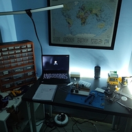
3/18/2026 - Assembling the AngstromIO and programmer
I finally received the PCB and components, and just realized how tiny they were... I mean, I knew the mini devboard would be smaller than 1cm², but it always looks bigger on the design on the screen, so... Anyway that is so cool!
I started assembling 2 AIO on one panel, carefully adding small blobs of solder paste with the seringe onto each pad (I didn't bought a stencil), and I add to make a few retouches with some tweezers and a small bit of tissue to remove the excess paste on some pads. I checked multiple times with my phone, realizing that with a 8x zoom, it can give pretty good results, a bit like a digital microscope, or at least it's still better than looking to the naked eye. Once I was satisfied, I populated 2 devboards, checking on the design files the orientation of the 1.5 by 1.5mm addressable LEDs (one of the two is rotated 90°) and added the few components on the top side (MCU (QFN20), resistors and capacitors (0402))
I then reflow soldered the boards on my hot plate, and had to use the tip of my soldering iron to remove the few solder bridges on the QFN IC. I really wanted to test the board before soldering the USB C on the other side, so... I assembled the programmer too. This time I snapped it directly from the panel, but other than that, it was the same process that followed: adding solder paste, placing the components while checking the orientation of the 0402 LEDs, reflow solder the boards, and retouch the solder bridges on the ICs (I had to remove one CH340 IC before putting it back on the PCB to get rid of the solder bridge on the D+ and D-, but it turned out easier that I thought, considering the legs on the MSOP-10 are quite long and close to each other).
I plugged the programmer on the computer, and it was recognized on the computer. Nice. After detaching the boards from the panel and sanding down the mouse bites, I then soldered thin-yet-bulky-compared-to-the-AIO cables to the mini devboard, on VBUS, GND and UPDI to try it right away, and uploaded the Arduino demo sketch on the AIO, and was really happy to see that it worked well, lighting up the 2 LEDs, meaning that the soldering process went really smoothly. Hurray!
Now that the top side is correctly soldered, I dealt with the other side, that while only having 3 discrete components, still scared me a bit because heating the bottom side up with the air gun could, and turned out it happened with an LED, make the components fall from the other side so I had to resolder it after (that's why double sided assembled PCB is usually done with two different solder paste, one with a higher temp that the other...)
Eventually I got the 2 AIO soldered, and finished the build by hand soldering the 4 legs USB-C, and that's where you understand why JLCPCB provides a 'Castellated holes' option, since the castellated holes made with the default process didn't turned out great... There were bits of copper everywhere in the hole but on the edges, but I still managed to solder the USB-C properly, even though the solder joins looked a bit weird with the tin sticking to the excess copper bits.
On one AIO, I ended up connecting wires on all the tightly packed solder pads, making it kinda breadboard friendly while completely defeating the purpose of having a small devboard, but I don't care since I'll certainly use this setup for prototyping with the ATtiny1616, so it's easier with the pins accessible. I kept the second AIO without any soldered wires, because it'll be used that way, and once the board is powered via the USB-C, it will be possible to program it directly by pressing a jumper wire to the UPDI pin, without any soldered programming wires... As long as there are common grounds, i.e. the devboard is connected via USB to the same device (laptop or power source) that the programmer.
... Actually you may remember that for the programmer to be powered, the 'Serial' (UART) side has to be connected to the PC, since it's the only USB-C providing power, so it means that with the AngstromIO connected too, I'll need 3 available USB ports on the host (the computer) for programming... So I might need to use a USB hub for my laptop...
And, that's official, I've measured the AIO dimensions. It's indeed 9mm long, but for the width, it's more 9.5 (instead of the 8.9) advertised, but it's just the solder join being too thick. I think that with the other boards I should be able to obtain the 9mm wide, using solder paste intead of manually soldering the 4 USB C legs.
Anyway that's enough talking, I'll let you appreciate this cute lil devboard, laying down on my index...
Gallery:
3/21/2026 - Coding the CH32 devboard demo
I coded the Demo code for CH32 devboard, which mainly consisted of handling the 5x4 charlieplexed LED matrix. I took a few functions from my IOX-77 project for the CH32, this way I could just focus on handling the matrix with the pinMode(), digitalWrite() and digitalRead() functions. Developing the code for the charlieplexed matrix was kinda mind-bending, but thanks to bitluni's explanation, I was able to create the required code for my 5x4 LED matrix... or at least I think it'll work as expected...
So basically, I've got a set of arrays, some containing the different LEDs configurations (like digits from 0 to 9), or an all-white and all-black array), which are used by the function updateDisplay() to display the image. it scans the display columns by columns (setting the corresponding column to LOW), and each row is driven simultaneously (HIGH or HI-Z)in accordance with the array in parameter. Each column is updated every DELAY_FRAME milliseconds, 2ms here, and the process is repeated over and over the number of times required to last duration ms.
I've created a small demo which uses all the features of this devboard: The orange LED on PC0 blinks until the button (PD0) is pressed, and then a countdown from 9 to 0 starts, ticking down every 1s. It then blinks the digit 0 two times before lighting all the LEDs up, to ensure they are all working correctly.
3/22/2026 - Assembling the CH32 devboard
I assembled one CH32 devboard, and adding the solder paste on all the pads was a tedious task, since I don't have any stencil. I think that for bigger LED matrices, I'll definitely buy a stencil. Anyway. I then placed all the components, making sure the 20 0402 LEDs were in the right orientation, and after reflow soldering the board, I tested it with the custom firmware right away: And I was really happy to see that everything worked first try! Even the Charlieplexed LED matrix! yay! ... when trying to hook the WCH Link-E to the devboard, I just noticed that I didn't had the TX UART pin broken out (I used it for the LED matrix), so I won't be able to get any Serial communication.
I then soldered pin headers (yeah, I know, the solder joins aren't perfect, especially for the PWR pins, but I forgot to add thermal reliefs, so it was kinda hard to get the solder to melt...)...
Anyway:
The board was ready for a small photoshoot...
Gallery
Small game: Can you spot the differences? 😂