DJI mic mini compatible usb c adaptor
replacement DJI mic mini usb C adaptor
Created by
 William 🚀
Tier 5
9 views
0 followers
 m0.hid ⚡
approved DJI mic mini compatible usb c adaptor ago
m0.hid ⚡
approved DJI mic mini compatible usb c adaptor ago
Tier approved: 5
Grant approved: $23.00
Great work on this, I love the animation that you made!
William 🚀
submitted DJI mic mini compatible usb c adaptor for ship review ago
 1mon ⚡
requested changes for DJI mic mini compatible usb c adaptor ago
1mon ⚡
requested changes for DJI mic mini compatible usb c adaptor ago
really cool project, its so compact, and great job on the journaling! your cart screenshots should include all of them items you are buying, please update this so we can see it! currently, the last screenshot doesnt show what the items are. please check out the submission guidelines https://blueprint.hackclub.com/about/submission-guidelines to make sure you are good to resubmit!
William 🚀
submitted DJI mic mini compatible usb c adaptor for ship review ago
William 🚀
added to the journal ago
Finished up the github repo
Wrote a hopefully ok GitHub readme

made sure I aligned all the images so it didn't look too clunky
Made another little animation to help with assembly
https://youtu.be/_XwIinutsPc
Also chose to add a licence, initially it was for the purpose of protecting me from liability if it doesn't work as intended and damages anything, originally the MIT licence was my go to but the GNU 3.0 licence ensuring that it stays open source is a cool little addon.
William 🚀
added to the journal ago
Errors, uh oh
From the top of the PCB it looks great

from the bottom it doesnt

those are some unhappy nets
Im tempted to remove the holes
and just SMD the terminal to the board instead of doing throughole
its not an idea situation
i should use this instead of butchering the THT into an SMD part

It looks good as a terminal

however, the inner gap between the posts looks like its around 4mm
which isnt enough to keep using the mounting mechanism i used to join the two halves
its also taller than the other part, by 1.2mm , which would mean the case has to be taller and wouldn't fit into the storage case
so I'm going to need to butcher the THT ones into being SMD
If I cut off the pink parts, it should behave like an SMD part

then this footprint should work

Ive updated the gerbers since making the changes
I also updated the PCB in CAD because the previous version had holes because of the THT components.
I also realised i could export the pads aswell so there are some extra angles


All I have left now is to create a BOM + a README.md
William 🚀
added to the journal ago
Polished CAD
I made the following changes
- rounded out the CAD with chamfers
- shortened the M3 bolt
- new way the case splits up
- made trimmed and untrimmed versions of the terminal
- created renders + animation


https://youtu.be/Vbs5DWWPDMo
it also loops in a cool way :3
William 🚀
added to the journal ago
Started work on creating a housing for the project
started off by importing the PCB from kicad as a .step

Then I opened the datasheet for the usb port and the terminal and used those to create a model for each of those


I used a pair of callipers to measure and model the screws i plan to use

putting it all together

well ,that looks like a problem.
yep it was an issue in the footprint, a quick adjustment and rotation later now it looks correct

There we go that looks a lot better

well i haven't seen fusion do that before

first finished CAD mock up


It prints in two parts
However it could do with some refinement and polish, i want to redesign the back end a bit so there arent still bits exposed on the sides,
The next version should have:
- correct length screws
- chopped and unchopped legs for the terminal
- chamfers on the outside to make it look cleaner
- a better way to clean up the outside
And optionally i could add a little logo that you could print with a multimaterial/colour 3d printer
William 🚀
added to the journal ago
More footprint work
fixing errors

I remembered that I couldnt leave all the pins as pin 1, that wouldnt be good
wooo fixed

back to working on the footprint for the other port
thought I was done at this point, but there are two rows of pins, oops

putting in two rows means my big pads don't exactly fit perfectly.

It looks like offsetting the pads works
andddd that looks good to me

onto the schematic
I plan to have the hole to have either of the configuration on 1 PCB, then you just solder 1, and maybe scratch off the unneeded traces


Turns out the space constraints wont let me have two connectors on one board
I also realised a fatal flaw with the USB-C connector sticking out at 90degrees
it wont fit in the case, which i think means i need to kill that off.
that leaves us with this
DRC comes out pretty clean

ive chosen to ignore a bunch of barely off edge clearances

this is the only problematic edge clearance, 0.13mm

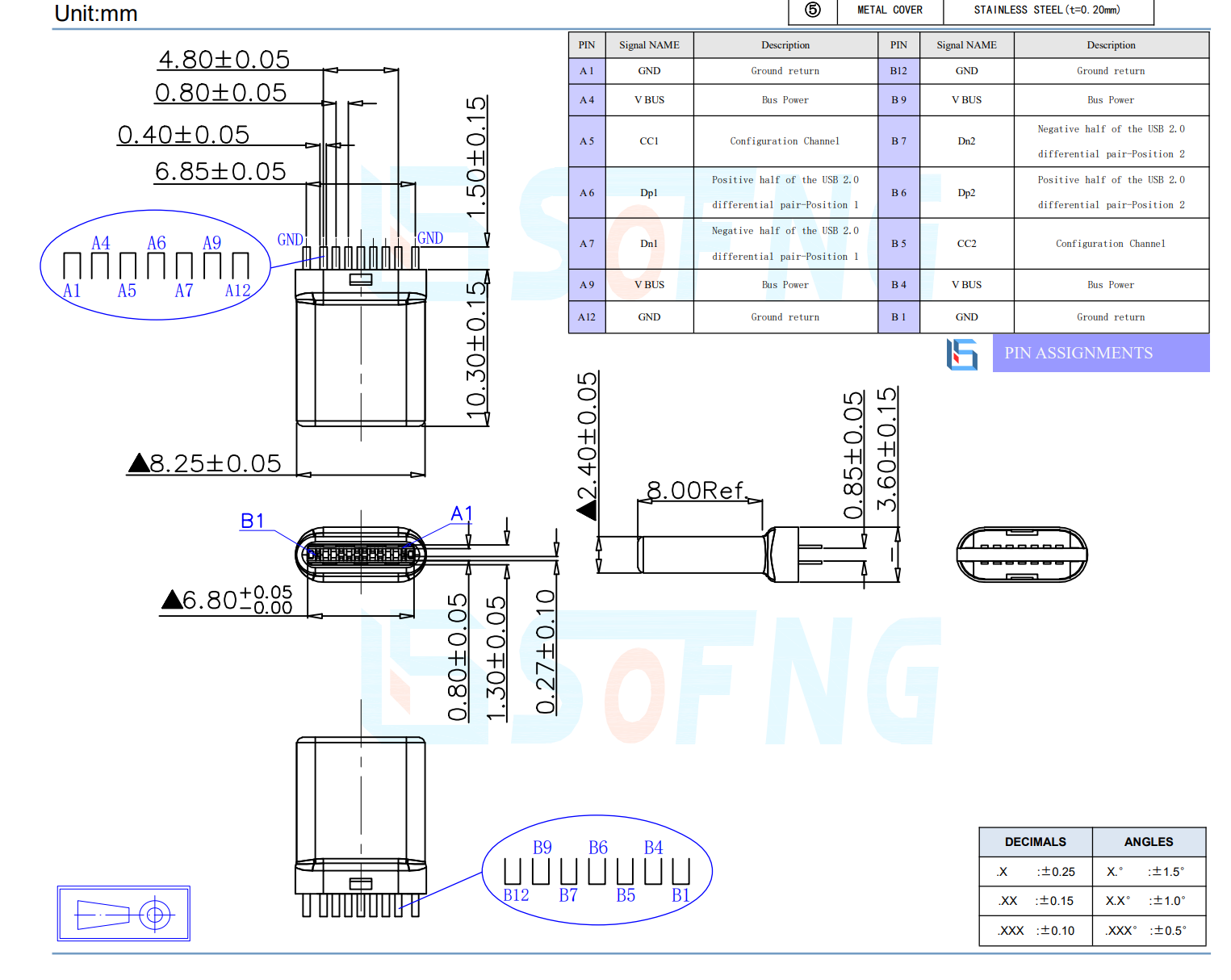
I remembered I should use a differential pair for D+ and D-

But I had so many issues with not being able to get kicad to do what I wanted I ended up manually matching the traces lengths to +-0.02mm , which is good enough for usb 2.0 spec


PCB looks pretty good now anyway
I also found this part, which has an M3 threaded hole

Its meant for terminals
However if i cut the legs short so they dont stick out the other side, then it works as a perfect way to attach things to my PCB


Then to screw into that I have these m3x6 wafer head bolts already on hand

William 🚀
added to the journal ago
Starting things in Kicad
Made the symbol + footprint for the connector in Kicad


thinking a bit about the pin i thought was NC
Im used to just chucking a 5.1K pull down resistor on each of the CC lines
Thinking about it a bit more its probably VCONN, and the one i marked as CC1 is the one thats used for configuration.
As to why they would would have it and add an extra pin i can only assume that one of the following situations is true
- its required for the apple lightning adaptor as that might require the 5v from VCONN to do some active circuitry, would also perhaps explain the price of that dongle
- someone at DJI preferred an even number of pins
- maybe its for some future expansion? although if it was needed for active circuitry, why not just piggy back of the 5v from VBUS ? Surely the DJI mic mini only requests 5V, adding PD would add complexity, its not like the mic mini could need more than 5V 3A.
Anyway
getting back to the design of the adaptor
i wanted to pick a USB connector that was ideally
- easy to solder
- cheap
- STRONG
I found some great options like this on LCSC


however it was the first two that stuck out to me. Their footprints seemed easier to solder, and i want to keep this project as accessible as possible.
making the footprint for the flat usb port
This took an embarrassing amount of time ( ~45min, I kept making mistakes and struggling to read the data sheet of it

I kept thinking the pin pitch was 0.59mm instead of 0.65mm, which then caused things to not align correctly and REALLY confuse me
here is the data sheet i was trying to follow for that

I ended up drawing it out and trying to solve the gaps

I was very confused ,but anyway,
as soon as I realised my mistake and set the pin pitch to 0.65mm it worked perfectly
making the the footprint for the other usb port option

for the vertical USB-C male port I chose a through hole design. The logic behind that decision was hopefully its harder to rip that out than ripping a pad off and SMD variant
The only cons of the specific connector I chose were :
- expensive for a usb port $0.4 for low quanities ( other ports ive bought in the past have been $0.10 )
- no recommended footprint
plenty of ways to connect them to things
- via a 3.5mm aux cable
- via a female usb port
- via a male usb attachment
A lovely range of connectivity
however that male port can be "tricky"


you might notice my dongle port not exactly being straight

when you plug it into a phone like intended its QUITE easy to accidentally donk it.
Best case you have a bent the the USB receptacle.
Worst case you have a dysfunctional or dismembered USB receptacle.
And if you want to buy a replacement
DJI don't sell them on their own

some third parties do, but $10-20 feels pretty expensive
my dongle got bonked, it looks like this


It shouldn't look like that.
However I'm lucky that mine still works, i want to reverse engineer it and make my own.
First step to trying to reverse engineering is working out what on earth is going on inside.
Since there isn't an apparent way to non-destructively open it up, a multimeter + continuity checkers was a good start.


This is what I believe the pinout is

there is also a resistance of 3.1ohms between gnd and cc1, which means that if they are using a 5.1k pulldown resistor, its in the receiver not in the little adaptor.
this means in theory all i need to do is create some sort of PCB that interfaces with the pogo pins and have a male USB type C port and it should work
My next step was trying to measure out what i need

A flatbed scanner gets me that wonderful hopefully orthograph photo of the dongle.
With a an easy to measure flat to flat measurement with callipers i can scale the image to know what outline my PCB should have
Currently making a rough mesh with meshroom as well as im interested what that will look like
William 🚀
started DJI mic mini compatible usb c adaptor ago
2/7/2026 - Did some stuff
just going to write a quick breakdown of the problem
recently i bought DJI mic minis
they are great!
Tiny size, tiny weight, massive battery battery life, sound good.
I love them.
plenty of ways to connect them to things
- via a 3.5mm aux cable
- via a female usb port
- via a male usb attachment
A lovely range of connectivity
however that male port can be "tricky"
you might notice my dongle port not exactly being straight
when you plug it into a phone like intended its QUITE easy to accidentally donk it.
Best case you have a bent the the USB receptacle.
Worst case you have a dysfunctional or dismembered USB receptacle.
And if you want to buy a replacement
DJI don't sell them on their own
some third parties do, but $10-20 feels pretty expensive
my dongle got bonked, it looks like this
It shouldn't look like that.
However I'm lucky that mine still works, i want to reverse engineer it and make my own.
First step to trying to reverse engineering is working out what on earth is going on inside.
Since there isn't an apparent way to non-destructively open it up, a multimeter + continuity checkers was a good start.
This is what I believe the pinout is
there is also a resistance of 3.1ohms between gnd and cc1, which means that if they are using a 5.1k pulldown resistor, its in the receiver not in the little adaptor.
this means in theory all i need to do is create some sort of PCB that interfaces with the pogo pins and have a male USB type C port and it should work
My next step was trying to measure out what i need
A flatbed scanner gets me that wonderful hopefully orthograph photo of the dongle.
With a an easy to measure flat to flat measurement with callipers i can scale the image to know what outline my PCB should have
Currently making a rough mesh with meshroom as well as im interested what that will look like
2/9/2026 - Starting things in Kicad
Made the symbol + footprint for the connector in Kicad
thinking a bit about the pin i thought was NC
Im used to just chucking a 5.1K pull down resistor on each of the CC lines
Thinking about it a bit more its probably VCONN, and the one i marked as CC1 is the one thats used for configuration.
As to why they would would have it and add an extra pin i can only assume that one of the following situations is true
- its required for the apple lightning adaptor as that might require the 5v from VCONN to do some active circuitry, would also perhaps explain the price of that dongle
- someone at DJI preferred an even number of pins
- maybe its for some future expansion? although if it was needed for active circuitry, why not just piggy back of the 5v from VBUS ? Surely the DJI mic mini only requests 5V, adding PD would add complexity, its not like the mic mini could need more than 5V 3A.
Anyway
getting back to the design of the adaptor
i wanted to pick a USB connector that was ideally
- easy to solder
- cheap
- STRONG
I found some great options like this on LCSC
however it was the first two that stuck out to me. Their footprints seemed easier to solder, and i want to keep this project as accessible as possible.
making the footprint for the flat usb port
This took an embarrassing amount of time ( ~45min, I kept making mistakes and struggling to read the data sheet of it
I kept thinking the pin pitch was 0.59mm instead of 0.65mm, which then caused things to not align correctly and REALLY confuse me
here is the data sheet i was trying to follow for that
I ended up drawing it out and trying to solve the gaps
I was very confused ,but anyway,
as soon as I realised my mistake and set the pin pitch to 0.65mm it worked perfectly
making the the footprint for the other usb port option
for the vertical USB-C male port I chose a through hole design. The logic behind that decision was hopefully its harder to rip that out than ripping a pad off and SMD variant
The only cons of the specific connector I chose were :
- expensive for a usb port $0.4 for low quanities ( other ports ive bought in the past have been $0.10 )
- no recommended footprint
![image](/user-attachments/blobs/proxy/eyJfcmFpbHMiOnsiZGF0YSI6MTAxMzExLCJwdXIiOiJibG9iX2lkIn19--35c3852122c45967841b34d216c690ae2b242c61/image.png
trying tyo make a footprint from this doesnt look fun
2/10/2026 8 PM - More footprint work
fixing errors
I remembered that I couldnt leave all the pins as pin 1, that wouldnt be good
wooo fixed
back to working on the footprint for the other port
thought I was done at this point, but there are two rows of pins, oops
putting in two rows means my big pads don't exactly fit perfectly.
It looks like offsetting the pads works
andddd that looks good to me
onto the schematic
I plan to have the hole to have either of the configuration on 1 PCB, then you just solder 1, and maybe scratch off the unneeded traces
Turns out the space constraints wont let me have two connectors on one board
I also realised a fatal flaw with the USB-C connector sticking out at 90degrees
it wont fit in the case, which i think means i need to kill that off.
that leaves us with this
DRC comes out pretty clean
ive chosen to ignore a bunch of barely off edge clearances
this is the only problematic edge clearance, 0.13mm
I remembered I should use a differential pair for D+ and D-
But I had so many issues with not being able to get kicad to do what I wanted I ended up manually matching the traces lengths to +-0.02mm , which is good enough for usb 2.0 spec
PCB looks pretty good now anyway
I also found this part, which has an M3 threaded hole
Its meant for terminals
However if i cut the legs short so they dont stick out the other side, then it works as a perfect way to attach things to my PCB
Then to screw into that I have these m3x6 wafer head bolts already on hand
2/10/2026 9 PM - Started work on creating a housing for the project
started off by importing the PCB from kicad as a .step
Then I opened the datasheet for the usb port and the terminal and used those to create a model for each of those
I used a pair of callipers to measure and model the screws i plan to use
putting it all together
well ,that looks like a problem.
yep it was an issue in the footprint, a quick adjustment and rotation later now it looks correct
There we go that looks a lot better
well i haven't seen fusion do that before
first finished CAD mock up
It prints in two parts
However it could do with some refinement and polish, i want to redesign the back end a bit so there arent still bits exposed on the sides,
The next version should have:
- correct length screws
- chopped and unchopped legs for the terminal
- chamfers on the outside to make it look cleaner
- a better way to clean up the outside
And optionally i could add a little logo that you could print with a multimaterial/colour 3d printer
2/11/2026 10 PM - Polished CAD
I made the following changes
- rounded out the CAD with chamfers
- shortened the M3 bolt
- new way the case splits up
- made trimmed and untrimmed versions of the terminal
- created renders + animation
https://youtu.be/Vbs5DWWPDMo
it also loops in a cool way :3
2/11/2026 11 PM - Errors, uh oh
From the top of the PCB it looks great
from the bottom it doesnt
those are some unhappy nets
Im tempted to remove the holes
and just SMD the terminal to the board instead of doing throughole
its not an idea situation
i should use this instead of butchering the THT into an SMD part
It looks good as a terminal
however, the inner gap between the posts looks like its around 4mm
which isnt enough to keep using the mounting mechanism i used to join the two halves
its also taller than the other part, by 1.2mm , which would mean the case has to be taller and wouldn't fit into the storage case
so I'm going to need to butcher the THT ones into being SMD
If I cut off the pink parts, it should behave like an SMD part
then this footprint should work
Ive updated the gerbers since making the changes
I also updated the PCB in CAD because the previous version had holes because of the THT components.
I also realised i could export the pads aswell so there are some extra angles
All I have left now is to create a BOM + a README.md
2/12/2026 - Finished up the github repo
Wrote a hopefully ok GitHub readme
made sure I aligned all the images so it didn't look too clunky
Made another little animation to help with assembly
https://youtu.be/_XwIinutsPc
Also chose to add a licence, initially it was for the purpose of protecting me from liability if it doesn't work as intended and damages anything, originally the MIT licence was my go to but the GNU 3.0 licence ensuring that it stays open source is a cool little addon.