Meko V2
A high definition music player with bluetooth support, which has an e paper display and a physical wheel V2
Created by
 koeg 🚀
Tier 1
152 views
8 followers
 alexren ⚡🚀
approved Meko V2 ago
alexren ⚡🚀
approved Meko V2 ago
Tickets awarded: 1329 tickets
Tier: 1
AWESOME JOB WOW HOLY SHIT KOEG
koeg 🚀
submitted Meko V2 for ship review ago
koeg 🚀
added to the journal ago
Made a ui

With a lot of help from copilot, I through to get her this ui, that allows you to select songs, see your progress, and pause your music. There was a reccuring error where something always made the ISR stack overflow, and make the program crash at runtime, this was really hard to figure out, it was something with how the display updates were handled. A lot of time was spent waiting for the bug to happen, and the interesting part was, when I was using my debugger to setup though the code, the error never came up.
Also you may notice that my cas doesn't look like shi anymore. I realized that I could print it at 45°, with minimal supports, and a really good surface finish.
I had to remodel how the display was retained, because how FDM printers print sharp corners, turns out they are not sharp, they are allowed rounded, and didn't allow the display to fit nice in it's place. The first image is the before, and the second is the after:


koeg 🚀
added to the journal ago
Got first working case

After a lot of failed version, most of them because clearance/tolerance issues, I got a case the works nicely, and fits all of the parts correctly, as expected
koeg 🚀
added to the journal ago
Got my dac finnally working!! And finished case in fusion
Electronics
I thought that I might have fried one of the output channels of my DAC, so I used one of my handy test pads on the other side of the PCB to use one of the unused output channels, I used the lead of a resistor as a bodge wire, because I didn't have anything else on hand:


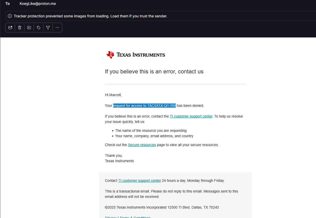
Right after this I reached out to TI's support again, because I have been waiting for their response on my request for their DAC config software. Turns out TI only gives out their proprietary software to companies and schools, so I needed to create a new TI account with my school email, and I got my request for the config software approved instantly!
The software is a GUI that generates the i2c commands to set up the DAC a certain way, but I think I'm not allowed to share screenshots because there was an NDA. But I think I can get away with this much:

Now I could pinpoint where I messed up in my driver code, and figure out why my right channel wasn't working.
Turns out, that by default the DAC doesn't send anything to the right channel, so I didn't burn out any output pin, I was just not routing the audio signal correctly. Now that I tested the new configuration, my audio sample played in both the left and right channels!!!!
Finally, all of my hardware works!
The case
I also finished redesigning the case:

The major issues I fixed, compared to the previous design, are that now there is enough space for the e-ink display's flex cable, I simplified the mounting of the display by not having a backplate, I switched to a larger cube magnet instead of the small round magnet, because the hall effect sensor was flaky, and left enough space for the battery by not using one of the mounting holes for screws.
Also, fusion is awesome! I can reference geometry from other bodies in sketches, and the software is a lot nicer to use all in all, and I can design a lot more quickly in fusion than in FreeCAD.
All I need to do now is to print out the case
I don't need AC coupling caps????!!!
I did some more research and my DAC had an output mode called pseudo-differential, which is almost the same as the single-ended mode, but the ground is not the system ground, instead a ground generated by the DAC, so in this mode, AC coupling caps are not needed:

This is great news, because I don't need to used giant 2200uF caps in V3, if that ever happens
koeg 🚀
added to the journal ago
Lots of small stuff
Finally decided to switch back to windows, Linux was just not working, I can just use WSL2 👍, and now I don't have to run a VM to use TI's software (I didn't count the time it took to install windows)

On the note of TI's software, they still didn't give me access to their gated ass software
I also tried out zephyrs threads, and put every separate hardware test in their own task. Also tried the partial update feature of my display, it works, but everything except the thing I'm updating fades. this may be because I'm still using the wrong inductor value.

I also tried to use LVGL PRO, a visual editor by lvgl, but it's really buggy, and just doesn't work, I wasted a lot of time with this. Along the journey of trying to get this thing working, I found out that the creator of lvgl is also Hungarian. I also tried SquareLine Studio, but that doesn't work with nordic chips.
Also, I made my inductor lie flat, instead of standing up, so I could make the final player thinner, I used the two wires of a tht resistor, to connect the inductor to the pads


I realized that I needed to adjust the dimensions of the case, to fit the new inductor, and to fix my misjudgments about how big the display's flexcable's stiffener would be. But every time I tried to change my design in freecad, even by 0.1mm, my assembly broke, or the program crashed. So I decided to redesign the case in fusion. I thought about using onshape, but in the future I want to use the generative design workbench of fusion for other projects, which onshape doesn't have.
koeg 🚀
added to the journal ago
TI and their gated software
Now that I'm 90% sure that I have a software problem with my DAC, I need to debug my driver. Turns out TI has software for configuring/testing their DACs/other audio stuff, it's called PUREPATHCONSOLE, it's like a launcher for other apps related to TI audio.
The only problem is that it is gated, you have to apply for you to download it. I got lucky and they accepted my request. Only problem is, that I still only had access to the "launcher" and none of the apps I wanted:

I wasn't as lucky with the actual app, they rejected my request:

And here is how I did it, see the missing caps and resistors?

But the datasheet doesn't give example values for these passives. So I took to electronics stackexchange, where I got some really helpful responses:


I learned that this cap acts like a high pass filter, so it filters out bass frequencies, and to decrease the amount of bass that is filtered out, you have to increase the size of the capacitor. And the cutoff frequency also depends on what the impedance of your load is, the smaller the impedance, like with headphones, the larger the cap.
Because this is a mp3 player, I'm mainly aiming to drive IEMs and headphones, so my cap has to be around 1000-4000uF to get a decent bass response, these large caps are usually really large, and only available in electrolytic types. Here comes in the humble Tantalum - Polymer Capacitor, these types of caps are really compact, and are great for audio, but relatively expensive.

Also did some research on what those resistors connected to ground do, and they are for mitigating popping sounds, and to bring the side of the caps connected to the headphones to ground.
For now, I can use a lot smaller caps for testing, my base response will be ass, but it will work. So I used an exacto knife to cut the traces that directly connected my DAC to the headphone jack. And I added some caps and resistors:


But the issues persisted, my PMIC still shut off when both of my IEMs were plugged in. So desoldered the left cap, and the right side played a white noise, with a hint of the sine wave.
So my next target was those ESD diodes, I removed those:

This solved one of my issues, the PMIC didn't shut off when both of my IEMs were plugged in. But the right IEM still didn't play the sine wave.
I used a small breadboard jumper to connect the left and right side of the DAC output, to see if I wired up the audio jack correctly, and both IEMs played the signwave, so my issue now is in software
koeg 🚀
added to the journal ago
The screen now actually works!
My new caps finally arrived from AliExpress, they are now actually rated for 25V, and are 4.7uF. I also stole the inductor off of my sister's Athena badge, because I also messed up the value of the inductor. I desoldered everything that I messed up:
 .
.
And then soldered the new components on (not my best works💀):

And now the screen isn't flaky, and works correctly:

koeg 🚀
added to the journal ago
Got output from the DAC!!
After I finished a testable version of the driver, this was mostly wrapping my head around how i2c works and how to configure the dac, I uploaded the firmware plugged int my IEMs, and... The MCU powered on, I heard a loud pop, and my PMIC restarted, and repeat
I tried messing with the sine wive that the DAC should have output, still the same issue.
I tried lowering the digital volume, still 😤
Finally, I disconnected the right side of my IEMs, and the sine wave actually played in the left bud!!!! So, now I tried only with the right bud, but heard nothing.
Now came a bunch of software debugging the didn't lead anywhere
The next step will be to look at my hardware at a deeper level, and figure out, if that's causing the problem!

koeg 🚀
added to the journal ago
Fighting with zephyr
I'm really struggling with writing this damn DAC driver, especially with the build system part, the actual C code isn't that hard, but all the surrounding tooling is killing me. It took me 2.5h to include my driver in my main application, make intellisense work and add it to the device tree.

Mentioning the device tree, I also added the LDO for the dac:

I also continued to write the actual code part of the DAC driver, I'm still at the configuration function, but now I kinda understand how zephyr handles stuff. Also, TI has excellent datasheets, with examples on how to get a working config, which I'm using as reference:


P.S. I wrote those comments, not ai
koeg 🚀
added to the journal ago
Started writitng the custom DAC driver

Turns out that writing a good driver in zephyr is really hard. There are literary no docs on how you should implement an audio driver, so you have to comb through other drivers to learn how you should write your own.
Also turns out that the DAC driver only configures the DAC, and you have to manage playback over i2s in your application code.
I started to write the initialization function, this sets up what audio format should the dac expect, what word length etc.
Created a new repo for the driver, and then I used zephyr's package manager to include it in my workspace. This is really fire because both my application code and driver code is in the same place, but in separate repos. The driver repo needed to be a zephyr module, so that took some time to figure out.
Without copilot/gemeni I couldn't have gotten this far, the docs are so ass 😭
koeg 🚀
added to the journal ago
Switched to a west workspace

Since I have to write my own driver for my DAC, switching to a west workspace is one of the easiest ways to separate out the driver into a separate repo, so other people can also use it, this also comes with the added benefit of the project managing what dependencies it needs, just like NPM, but for C.
This took some time, because the container that I was developing in just snapped out of existence, so I had to set that up again, I had made an image, but I didn't update that with my changes, so it was easier to just make a new one.
Also, the west workspace broke some stuff, like the build system not picking up my board definitions and zephyr not finding some libraries.
Copilot comes in clutch with decoding the 1000+ line error messages
koeg 🚀
added to the journal ago
Ordered a new display and capacitors

I ordered a new e ink display,so that I can be sure that my PCB was at fault, and new 4.7uF caps that are actually rated for 25V. They are already at the airport.
After I ordered them, I realized that I also messed up the inductor
value for the display, as in the inductance is correct, but the saturation current isn't, I used a 170mA inductance one instead of a 500mA inductance one. But I'm going to order this with the new hardware grant in the shop
koeg 🚀
added to the journal ago
READING!!!!


I started to dive into how zephyr handels device drives, because I need to write a driver for my DAC (TAD5212). Without Nordic's courses, I would be cooked, zephyr has ass docs.
I also started looking into how the TAD handles registers. Bad news there are like 250 of them💀
I also read how zephyr handles DFU, and multi threading on a more advanced level, and read some parts of the ble course
koeg 🚀
added to the journal ago
SD card works

I used a bunch of example from Nordic to get this working. I formatted the SD card to use the FAT file system, and put a simple text file onto it. And then used the sd_card_list_files function to get the files on the card. But nothing showed up, so I spent a lil bit of time debugging the firmware, and still nothing. Turns out the file system on the SD card got corrupted, so I formatted it again, put another file on there, and now it worked.
I think I should buy a book on zephyr, because there are a lot of universal APIs that are not explained really well, but are really powerful, and a good book would solve this, if it even exists.
koeg 🚀
added to the journal ago
Got the hall sensor working

Luckily zephyr already had a driver for this IC, but it can't read the output pin of the sensor , only read the i2c register, so I will have to rewrite this later. But it was pretty easy to implement, it uses zephyr's standardized sensor API
koeg 🚀
added to the journal ago
Display is really flaky
Right after I made the journal entry about the display working, it started to show the exact same behavior

After a lot of changing around small stuff in the code, I realized that I messed up a value of a cap in the boost converter section of the display's supporting circuitry, I used a 1uF/10V cap instead of a 4.7uF/25V cap. Luckily I had 4.7uF caps from Meko V1. So I took off the 0603 1uF cap and soldered in its place a 4.7uF cap (It's the one between the transistor and a diode):

But just after I soldered it one, I checked if the voltage rating was above 25V. It wasn't...
So I checked both the designs of Meko V1 and my split keyboard, if I used 1uF or 4.7uF caps that were rated above 25V. I didn't :yay:
Just for testing, I powered on the PCB a few times, and one time it worked, but then right after it returned to being borked:

Also I tested if prevgh and prevgl were the right voltage, the were at -+19V, which is in range. Shout out to MPK for suggesting this test.
But there is still a chance that my display is broken, so I will buy another one just in case.
But for now, I will continue work on other part's of the firmware
koeg 🚀
added to the journal ago
The EPD works

I found an example on how to configure RTT logging properly with the Segger Jlink, and when I applied these changes the screen turned black, which means it was working???? IDK what's the connection between logging and the screen driver, but I'm really happy that it works. I still had to mess around a bit, and learn how LVGL actually works, because at first as mentioned, the EPD turned fully black, I had to actually check if I could output text to the display.
In conclusion, if you do your configuration right with zephyr, everything works like a charm, but if you mess something up, you are up for a ride.
The next low hanging fruit is the hall effect sensor, and then the SD card, but it should be pretty easy to check if they are working.
Also, bad news, it turns out that there is no zephyr driver for my DAC. So I started researching on other implementations of this driver, that are not for zephyr. The first result that came up was from the Linux kernel, so that might be worth investing further. But other than that, the rest of the results were not as useful.
koeg 🚀
added to the journal ago
Got my pmic working

Got my PMIC up and running, I can communicate with it, control the regulators, control the LEDs, etc. It was pretty easy
On another note, I got a reply on the EPD support ticket, so I will have to try out what the agent said.
On another another note, turns out my vibration motor was sucking a lot of power, so I literally turned my DC 3V3 rail into a 2.5-3v3 AC line 💀 So I thought that's why my EPD stopped working, so I tried turning of the motor, and using the EPD, still nothing, and no response from the screen. So it's still dead
koeg 🚀
added to the journal ago
This epd is killing me

It turns out that I got that weird error because my epd (e-paper display) wasn't actually connected to my PCB, and that causes an error in the TF-M core, in a thousand years wouldn't have I thought that that could have been the cause. Now that I could run code with the display driver not messing with things, so I tried using LVGL to put a simple line of text on the screen. This sounds simple, but the universe hates me IG and if I tried to interact with the display my program just crashed in an unknown place :yay: One time though It put some random dots on the screen, see image. After like 4 hours of debugging and changing/checking my code line by line, I might have broken my display, because code that worked previously just doesn't work. Also, there was a side quest where zephyr didn't print to the console, so that was fun, and I still don't know the full cause, life is fun isn't it.
I will try some new stuff tomorrow to see if I actually killed the screen, but w'ill see.
Also, I continued to read the Nordic zephyr guide

koeg 🚀
added to the journal ago
Finshed lesson 7 on nordic dev academy

In this lesson I learned how zephyr handles basic multithreaded applications, the basics of how the scheduler works, and when and how to use work queues to not starve other threads.
koeg 🚀
added to the journal ago
Started implementing the npm1300 pmic
The situation is very similar to other drivers in zephyr, no docs, I made a kinda ok device tree structure, ̶b̶u̶t̶ ̶I̶ ̶c̶a̶n̶'̶t̶ ̶s̶e̶e̶m̶ ̶t̶o̶ ̶f̶i̶n̶d̶ ̶h̶o̶w̶ ̶t̶o̶ ̶u̶s̶e̶ ̶t̶h̶e̶ ̶l̶o̶a̶d̶ ̶s̶w̶i̶t̶c̶h̶ ̶f̶e̶a̶t̶u̶r̶e̶ ̶o̶f̶ ̶t̶h̶e̶ ̶n̶p̶m̶1̶3̶0̶0̶ so I made a support ticket for this issue as well, this service of nordic is awesome!!!
EDIT: Found the option

koeg 🚀
added to the journal ago
I think I'm going to jump off a bridge
With the vibration motor working, I wanted to tackle something bigger, so I started implementing the e-ink display. It turned out that zephyr already had a driver implementation for my display :yay: . This meant that I didn't have to muck around with implementing the driver myself. The problem was that zephyr doesn't have that great of a documentation for drivers, almost literally none, so I spent a long time figuring out how the device tree node worked and what was needed to get LVGL working with my display. After 4 hours, I had a minimal device tree setup, and I went to flash the new firmware to my PCB.

After I flashed it, the vibration motor didn't start vibrating, which it was supposed to do, WTF. I flashed it again, but in debug mode, to see what was happening:

An exception was thrown in the TF-M side of the firmware (on modern arm SoCs there is a feature called Trust Zone which splits up your firmware into two parts, a secure one, where sensitive info and cryptography lives, and an unsecure one, where your application code, RTOS and BLE stack lives, this is the recommended way to build firmware, TF-M is the zephyr implementation of Trust Zone).
When this happened, I didn't know anything about TF-M or WTF was happening, so it took me a really long time to understand all TS. The most likely cause of this is that the display node in my device tree messes with the application configuration, and the stack sizes, or causes a stack overflow, TBH IDK, I submitted a ticket on Nordic's support platform.
I also tried to build without TF-M, but that also didn't work, but IDK if I messed something up while I configured this new build.
I'm putting the e-ink screen on pause for now, and starting to implement my power management IC
koeg 🚀
added to the journal ago
Got zephyr up and running
Containers, Containers, and Containers
Turns out that in Bazzite if you want to do anything, you have to use a container, I know about this, but didn't know that it would go to this extent. When I first tried to install the nRF connect SDK, not in a container, it just gave me an error, this is because Bazzite is immutable. The solution: Run an Ubuntu container in which you install all the dependencies of your project, and forward the USB programmer to the container.

In hindsight this may sound simple, but I spent 2.5 hours figuring this out, along the way I learned what podman is, it's like docker just a lil bit different, and Bazzite runs on TS.
The zephyr experience
Zephyr is HARD, I had to reread the docs soooo many times, but once you understand it, it's GOATed. The nRF connect SDK is amazing, "it just works" TM. It has a bunch of devtools, and you can visualize your device tree:

Getting the vibration motor and buttons working
Now with my new-found knowledge of zephyr, it was time to do some testing, so I got the vibration motor working. This was a huge win for me, this was the first time I put my own code on my own custom PCB!

koeg 🚀
added to the journal ago
THE PCB ARRIVED!!!


The only thing I needed to do now is test it out! I needed to solder the 5x2 SWD programming header. But there is a problem, the pitch is 1.27mm, which is minuscule, so I did a few practice runs on the non assembled PCBs:

All of them I failed. There was always some tiny speck of solder connecting two pins. The solution: Don't solder the header.
I put the header in the JLink cable, and put that in the holes in my PCB, and twisted it, so there was some tension, so all the pins connected with the pads.

I downloaded the JLink software again (switched to Bazzite from Fedora), and tried to connect to my MCU.
Connection failed...
Turns out I didn't apply enough tension to make good contact with all the pins. And now... Successful connection

koeg 🚀
added to the journal ago
Realized that I dont know C
While I continued to read the Nordic dev academy course, I realized that I don't know C. I know a bit of C++, but it turns out that they do a lot of things very differently in C, so I started to watch a C course. I'm currently watching it a 1.75x speed 💀 because the guide goes over very beginner stuff as well.
The guy mentioned the natural logarihum function, so I also learned what e is, and what the natural logarithm is, and then went deeper in the rabbit hole and learned what Euler's identity is. 

koeg 🚀
added to the journal ago
3D printed the case for visualization


So far I have only seen the case on a computer screen, so I quickly 3D printed one on my FDM printer. The tolerances aren't quite there, but this is expected.The final part will be resin printed
 Josh
gave kudos to Meko V2 ago
Josh
gave kudos to Meko V2 ago
Cool idea!
koeg 🚀
added to the journal ago
Getting sponsored by JCL?? (and that's not a typo)
This all started when I asked for a design review on the r/PrintedCircuitBoard subreddit, and a Redditor replied in broken English that they will manufacture my PCB for free. (The mods have removed the comments since then)

I was really hesitant at first, they DMed me on Reddit, and asked for my phone number so we can continue on WhatsApp. Now I thought, this 100% must be a scam, but I continued. I didn't give them my phone number, just my email. In the email convo I found out that this is in fact a real company in China, and that they have an Alibaba store, and that they would give me free PCBs, assembly and shipping, I just needed to pay for the parts. They wanted my to use their Alibaba store to place an order, which was nice since if it was a scam, I could just ask for my money back.
So just a recap, someone in broken English replied to my Reddit post, and now I'm getting free pcbs??? WTF
This doesn't end here. My contact Elle, really nice person, offered me to do some design jobs, crazy. I declined these though, because the wage was really low.
Today they sent out the pcbs:

koeg 🚀
added to the journal ago
Learinig zephyr

Finished lesson 2 and 3. Zephyr seems really powerful, but it's really complex. I still have not grasped all the core concepts in the guide, the device tree is hard.
koeg 🚀
added to the journal ago
Learning zephyr

Started learning zephyr, to be more specific the nRF SDK, they have excellent docs, but it introduces a lot of new concepts, so I'm slowly reading through it.
Also, my J-LINK arrived. Thanks Niko from Segger for sending it out!!!!
 CAN ⚡🚀
approved Meko V2 ago
CAN ⚡🚀
approved Meko V2 ago
Tier approved: 1
Grant approved: $281.00
Holy this is so fire
koeg 🚀
submitted Meko V2 for ship review ago
koeg 🚀
added to the journal ago
Made new renders, removed some load caps
I updated the old renders, with the new pcb and case. Also realized that i could remove the load caps from my 32MHz crystal, because the nrf53 has ones built in. I also changed out the 32.878kHz crystal, to one that has a 7pF load capacitance, the prev one had 12pF, and the nrf53 only has 5pF, 7pF and 9pF internal load caps.

 nimit ⚡🚀
requested changes for Meko V2 ago
nimit ⚡🚀
requested changes for Meko V2 ago
Awesome project and absolutely lovely renders! I hate to ask this, but could you please add your schematic and PCB screenshots to the README? A significant part of the design was put there and it's required in the README! Just go through the submission guidelines to find everything you need.
koeg 🚀
submitted Meko V2 for ship review ago
koeg 🚀
added to the journal ago
Reduced BOM, fixed clearance issue

While getting a quote at jlc, I noticed that the footprint for my motor was misleading, and its courtyard wasn't as big as it was supposed to be, so it interfered with a resistor, so i moved that.
Also switched out a bunch of passives from the extended lib to the basic library as requested. It reduced the BOM by 22$.
CAN ⚡🚀
requested changes for Meko V2 ago
Is it all possible to use components for economic rather than standard PCBA? it is much much cheaper
koeg 🚀
submitted Meko V2 for ship review ago
koeg 🚀
added to the journal ago
Removed nRF DK from bom
I removed the nRF DK from the BOM, because tools aren't allowed. I'm gonna be bankrupt after TS😭 But I hope that it will last a long time and I can use it in the future .jpeg)
 technical_.
requested changes for Meko V2 ago
technical_.
requested changes for Meko V2 ago
Returned due to EVAL board in cart.
koeg 🚀
submitted Meko V2 for ship review ago
koeg 🚀
requested changes for Meko V2 ago
Didn't upload all cart screenshots
koeg 🚀
submitted Meko V2 for ship review ago
koeg 🚀
added to the journal ago
Added missing links to bom
Added missing links to bom for the NRF54L15-DK from Digikey, and the IDC cable for SWD debugging and flashing from AliExpress, that I will connect to my PCB and the nrf dk.

 Shaurya Bisht
requested changes for Meko V2 ago
Shaurya Bisht
requested changes for Meko V2 ago
can you add sources in your bom
koeg 🚀
submitted Meko V2 for ship review ago
koeg 🚀
added to the journal ago
Prepped for blueprint submition
Added LCSC part numbers, and updated outdated mrf part numbers. Updated the bom and readme. Changed out a few parts, like some inductors, and capacitors.

koeg 🚀
added to the journal ago
Modified case and pcb
I realized that I didnt place the power button and audio jack in the correct place, so i moved them. Updated the case with the new mouting hole, sd card, and jack positions.


koeg 🚀
added to the journal ago
Datasheet reading
Most of my was spent rereading all the datasheets. Along the way I found a small issue in the hall effect IC circuit, was a quick fix, just had to connect the 5v and 3v inputs. Also, someone pointed out that in the nrf53 reference pcb layout, there is a cutout in the GND plane beneath the feed line, turns out this is to make the feedline thicker, while keeping the impedance at 50 ohms. This is good to make the feedline thickness closer to the width of the pads of the matching components, so there is less impedance mismatch, also it reduces resistance. Also found out that the nrf53 has internal load capacitors for its crystals, so you can tune the values without needing to resolder the caps, which is nice for RF.


koeg 🚀
added to the journal ago
Finished routing traces pcb

I placed all the testpoints, added some 3d models. I still have to add the rest of the 3d models. I had to reroute some of the traces, cuz of the tespoints
koeg 🚀
added to the journal ago
Finished routing traces

Finished routing rest of the traces, changed recalculated the antenna trace impedance, still need to place testpoints and assign some 3d models, placed stiching vias
koeg 🚀
added to the journal ago
Routed more traces

Only 26 unrouted traces left, and placing the testpoints
Laid out the antenna, asked about on the kicad discord, discussing it right now, might have to move stuff around
koeg 🚀
added to the journal ago
bunch of routing


Did a bunch of routing. Redid the layout of the analog section for easier routing as well, routeated the dac 45 degrees so the two analog sides can be on the analog side of the via fence and the two digital on the digital side of the via fence.
Moved a bunch of pin assignments on the nrf for easier routing
koeg 🚀
added to the journal ago
Routed a bunch of traces

I routed a bunch of traces, including usb, microsd, and the display. I moved pins around on the mcu so it's easier to route.
Furthermore, I also choose the stack up, I'm going with a 6 layer board, the jlc basic one with two cores, so my stackup is sig/gnd/sig/gnd/gnd/sig, so every layer has a close GND layer.
I also turned on teardrops, and test the curvy traces plugin and it looks awesome

koeg 🚀
added to the journal ago
removed caps from software controlled buttons, placed jumper
I saw a video that said controlled buttons debouncing caps are useless at best and shorten the lifespan of your buttons at worst, so i removed all the caps from the software controlled buttons. Also laid out the rest of the jumpers, only the testpontints left, th
at I'm going to leave to the end
koeg 🚀
added to the journal ago
finished first pass of rough layout


i still need to add 3d models, and place all the testpoints, some jumpers and the swd connector
I will stay with this package i think, it will be fun to be able to use small vias like ts
 Tanuki ⚡🚀
gave kudos to Meko V2 ago
Tanuki ⚡🚀
gave kudos to Meko V2 ago
This is sick
koeg 🚀
added to the journal ago
Almost finished with basic layout


This is a rough layout, just to help me visualize how I should proceed
Still contemplating using a module for the nrf53, seems easier, and if i want to sell this later on i wouldn't have to get rf certification
koeg 🚀
added to the journal ago
Changed out the parts that were not avalibile on lcsc


I still had some parts that were not avalabile on lcsc from v1, so i looked for new parts, I changed out the usb port, display fpc port, vibration motor
koeg 🚀
added to the journal ago
Added a butt ton of testpoints

I also added a bunch of jumper pads on the i2c lines, so i can isolate one component if i want too. In the same way I also added jumper pads on the power of the chips, so i can just disconnect them

Im staying with the nrf53, because the nrf54l doesn't have audio pll, so small vias it is
I found a bug, I connected the i2c address pad of the dac to a gpio, now i have two options for and address

koeg 🚀
added to the journal ago
Rethinking how to make this prototype PCB
I was worried on the size of the pcb, make it as small as possible. With V1, this came to my demise. In v2 the main goal will be to be able to fix mistakes that I made, so I will leave spacing between components, put a bunch of test pints and bridgeable/cuttable test pads, and not worry myself about the size of the final product. If this prototype works, I will shrink everything down for production.
I'm also reconsidering the nrf54l, which is available in a qfn package, but most likely I will stay with the nrf53

koeg 🚀
added to the journal ago
Chat I might be cooked
My pmic is not available in a qfn package at lcsc, only in bga😭 First bga that I will use every, so I watched a bunch of altium academy videos about bga design. Also I need 0.2/(0.3)mm vias for both the pmic and the nrf53, so 5 PCBs will cost around 69$ (nice). I also checked how much would double sided PCBA will cost, it's around 210$ USD for two PCBs. So tier 1 here I come!
I'm pretty scared that this won't work like V1, so I'm putting extra effort in to quadruple-check everything. I will also place a frick ton of test points.

koeg 🚀
added to the journal ago
added leds to the pmic


Made final touches to the schematic, added leds to the pmic, double-checked everything one more time. Added some more testpoints, but i will add a lot more.
I'm debating doing double-sided pcba, but IDK if I will fit in the budget
koeg 🚀
added to the journal ago
Switched out DACs


I posted my design on the kicad discord for review, and the people there pointed me in the right direction about my DAC. The ESS DAC that I was using was expensive and hard to implement, I switched to the TI TAD5212 which has the same performance, and is a lot easier to implement, and has a bunch more features, and it's half the price at $5, and it's also available at lcsc, so I can get PCBA.
I spent a lot of time reading the datasheet
I also switched out some parts from v1 that were not available at lcsc that are available.
The schematic is almost done, the last thing i might add are some charging indicator LEDs to the pmic.
koeg 🚀
added to the journal ago
Many small changes
I went over the schematic again, fixed some stuff.
I used mouser for v1, and i plan to use lcsc for v2, so i replaced the parts that lcsc doesn't have, except my amp/dac, I will solder that to the PCB using hot air reflow. Furthermore, I also moved from an externally powered oscillator to a plain old crystal for my dac, it's just simpler this way. Changed footprints from 0402 to 0603 for better debugging
koeg 🚀
added to the journal ago
Finshed rough shematic

I finished the power train. Connected everything to the soc. Removed/separated a bunch of nets from v1, where I was in a shortage of pins, so i combined reset pins and similar things. Switched over to spi from sdio for the sd card. Made the schematic prettier
koeg 🚀
added to the journal ago
Reread the datasheet of my AMP/DAC chip
In v1 i used 1mm1mm power regulators for my audio chip, which were hell to debug/hand solder. SO this time I'm using almost the same regulator from TI, but in a 3mm3mm sot-23-5 footprint. I reread the datasheet of my audio chip, and realized that I don't actually need one of those regulators, so I'm now two regulators down, the other that I removed was my general 3.3v regulator, because the npm1300 has one built in.

Also, my hall effect sensor for my dial draws a lot of idle current, so I utilized one of the load switches of the npm1300(my beloved) to no give power to it when the device is in sleep mode
koeg 🚀
added to the journal ago
Started to redo schematic
Deleted a whole bunch of components. Added in the nrf5340 and all of its surrounding circuitry. Also added the npm1300, I'm so excited to use this bms btw (≧▽≦) removed the old BMS, some of the regulators, because the BMS has built in ones. IDK if I should use 1.8V logic or 3.3V logic though


koeg 🚀
added to the journal ago
Found my dream BMS
I just found out that Nordic makes BMSs specially for the nrf5 series, it's called the npm1300, so they have full example schematics of the two working tougher!! It also has fuel gauge functionality, and is able to monitor every voltage in the system. It has two voltage regulators built in, that you can also control with i2c. It has native support for USB power negotiation. It also seems pretty easy to implement.

Most of my devlogs so far have been doing research😭
koeg 🚀
added to the journal ago
Realized that the nrf5340 exists
Realized that nrf has much better documentation, more examples and a better rtos. It has less ram than the stm32, but it is much more power efficient.
I have worked with the nrf52840 before, and it is almost the same. I'm just worried about routing the second row/layer of pins on the package

koeg 🚀
added to the journal ago
Looking for an SoC that has bulilt in USB controller
V1 had a few issues, one of them that there had to be a whole separate chip to convert from usb to uart for the esp32 (gen 1), and in general it is kinda hard to flash a first gen esp32.
But the problem is that from my research the only SoC that has Bluetooth audio, and wifi is the first gen esp. So v2 probably won't have Wi-Fi, so no Spotify/other streaming. Which is kinda sad, but I rather have a less feature packed project, then a project that is not in a working condition like v1.
So far I have landed on the STM32WBA65CI, it has ble 6.0 and audio support, its beefy, has plenty of io, and most importantly an integrated usb controller. Maybe for a next version I will add an esp32c3 has a Wi-Fi module, but first this has to work
Also, some other stuff that I have been thinking on changing/leaving for v2:
- I will not use 0402 components, and other small components in general, it's just a pain to debug and work with, once I have a working prototype, I can do a version with small components
- Simplify the power and battery systems, I won't use a power path and a fuel gauge chip, just a tp bms and a voltage divider for the battery percentage
- I am leaving the DAC/AMP chip, and all the surrounding circuitry, except I'm using larger package sizes for the accompanying components

koeg 🚀
started Meko V2 ago
9/30/2025 - Looking for an SoC that has bulilt in USB controller
V1 had a few issues, one of them that there had to be a whole separate chip to convert from usb to uart for the esp32 (gen 1), and in general it is kinda hard to flash a first gen esp32.
But the problem is that from my research the only SoC that has Bluetooth audio, and wifi is the first gen esp. So v2 probably won't have Wi-Fi, so no Spotify/other streaming. Which is kinda sad, but I rather have a less feature packed project, then a project that is not in a working condition like v1.
So far I have landed on the STM32WBA65CI, it has ble 6.0 and audio support, its beefy, has plenty of io, and most importantly an integrated usb controller. Maybe for a next version I will add an esp32c3 has a Wi-Fi module, but first this has to work
Also, some other stuff that I have been thinking on changing/leaving for v2:
- I will not use 0402 components, and other small components in general, it's just a pain to debug and work with, once I have a working prototype, I can do a version with small components
- Simplify the power and battery systems, I won't use a power path and a fuel gauge chip, just a tp bms and a voltage divider for the battery percentage
- I am leaving the DAC/AMP chip, and all the surrounding circuitry, except I'm using larger package sizes for the accompanying components
10/8/2025 - Realized that the nrf5340 exists
Realized that nrf has much better documentation, more examples and a better rtos. It has less ram than the stm32, but it is much more power efficient.
I have worked with the nrf52840 before, and it is almost the same. I'm just worried about routing the second row/layer of pins on the package
10/15/2025 - Found my dream BMS
I just found out that Nordic makes BMSs specially for the nrf5 series, it's called the npm1300, so they have full example schematics of the two working tougher!! It also has fuel gauge functionality, and is able to monitor every voltage in the system. It has two voltage regulators built in, that you can also control with i2c. It has native support for USB power negotiation. It also seems pretty easy to implement.
Most of my devlogs so far have been doing research😭
10/16/2025 - Started to redo schematic
Deleted a whole bunch of components. Added in the nrf5340 and all of its surrounding circuitry. Also added the npm1300, I'm so excited to use this bms btw (≧▽≦) removed the old BMS, some of the regulators, because the BMS has built in ones. IDK if I should use 1.8V logic or 3.3V logic though
10/20/2025 9 PM - Reread the datasheet of my AMP/DAC chip
In v1 i used 1mm1mm power regulators for my audio chip, which were hell to debug/hand solder. SO this time I'm using almost the same regulator from TI, but in a 3mm3mm sot-23-5 footprint. I reread the datasheet of my audio chip, and realized that I don't actually need one of those regulators, so I'm now two regulators down, the other that I removed was my general 3.3v regulator, because the npm1300 has one built in.
Also, my hall effect sensor for my dial draws a lot of idle current, so I utilized one of the load switches of the npm1300(my beloved) to no give power to it when the device is in sleep mode
10/20/2025 11 PM - Finshed rough shematic
I finished the power train. Connected everything to the soc. Removed/separated a bunch of nets from v1, where I was in a shortage of pins, so i combined reset pins and similar things. Switched over to spi from sdio for the sd card. Made the schematic prettier
10/21/2025 - Many small changes
I went over the schematic again, fixed some stuff.
I used mouser for v1, and i plan to use lcsc for v2, so i replaced the parts that lcsc doesn't have, except my amp/dac, I will solder that to the PCB using hot air reflow. Furthermore, I also moved from an externally powered oscillator to a plain old crystal for my dac, it's just simpler this way. Changed footprints from 0402 to 0603 for better debugging
10/26/2025 - Switched out DACs
I posted my design on the kicad discord for review, and the people there pointed me in the right direction about my DAC. The ESS DAC that I was using was expensive and hard to implement, I switched to the TI TAD5212 which has the same performance, and is a lot easier to implement, and has a bunch more features, and it's half the price at $5, and it's also available at lcsc, so I can get PCBA.
I spent a lot of time reading the datasheet
I also switched out some parts from v1 that were not available at lcsc that are available.
The schematic is almost done, the last thing i might add are some charging indicator LEDs to the pmic.
10/27/2025 - added leds to the pmic
Made final touches to the schematic, added leds to the pmic, double-checked everything one more time. Added some more testpoints, but i will add a lot more.
I'm debating doing double-sided pcba, but IDK if I will fit in the budget
10/28/2025 1 AM - Chat I might be cooked
My pmic is not available in a qfn package at lcsc, only in bga😭 First bga that I will use every, so I watched a bunch of altium academy videos about bga design. Also I need 0.2/(0.3)mm vias for both the pmic and the nrf53, so 5 PCBs will cost around 69$ (nice). I also checked how much would double sided PCBA will cost, it's around 210$ USD for two PCBs. So tier 1 here I come!
I'm pretty scared that this won't work like V1, so I'm putting extra effort in to quadruple-check everything. I will also place a frick ton of test points.
10/28/2025 11 AM - Rethinking how to make this prototype PCB
I was worried on the size of the pcb, make it as small as possible. With V1, this came to my demise. In v2 the main goal will be to be able to fix mistakes that I made, so I will leave spacing between components, put a bunch of test pints and bridgeable/cuttable test pads, and not worry myself about the size of the final product. If this prototype works, I will shrink everything down for production.
I'm also reconsidering the nrf54l, which is available in a qfn package, but most likely I will stay with the nrf53
10/28/2025 8 PM - Added a butt ton of testpoints
I also added a bunch of jumper pads on the i2c lines, so i can isolate one component if i want too. In the same way I also added jumper pads on the power of the chips, so i can just disconnect them
Im staying with the nrf53, because the nrf54l doesn't have audio pll, so small vias it is
I found a bug, I connected the i2c address pad of the dac to a gpio, now i have two options for and address
10/28/2025 10 PM - Changed out the parts that were not avalibile on lcsc
I still had some parts that were not avalabile on lcsc from v1, so i looked for new parts, I changed out the usb port, display fpc port, vibration motor
11/5/2025 - Almost finished with basic layout
This is a rough layout, just to help me visualize how I should proceed
Still contemplating using a module for the nrf53, seems easier, and if i want to sell this later on i wouldn't have to get rf certification
11/6/2025 - finished first pass of rough layout
i still need to add 3d models, and place all the testpoints, some jumpers and the swd connector
I will stay with this package i think, it will be fun to be able to use small vias like ts
11/12/2025 - removed caps from software controlled buttons, placed jumper
I saw a video that said controlled buttons debouncing caps are useless at best and shorten the lifespan of your buttons at worst, so i removed all the caps from the software controlled buttons. Also laid out the rest of the jumpers, only the testpontints left, th
at I'm going to leave to the end
11/15/2025 10 AM - Routed a bunch of traces
I routed a bunch of traces, including usb, microsd, and the display. I moved pins around on the mcu so it's easier to route.
Furthermore, I also choose the stack up, I'm going with a 6 layer board, the jlc basic one with two cores, so my stackup is sig/gnd/sig/gnd/gnd/sig, so every layer has a close GND layer.
I also turned on teardrops, and test the curvy traces plugin and it looks awesome
11/15/2025 11 PM - bunch of routing
Did a bunch of routing. Redid the layout of the analog section for easier routing as well, routeated the dac 45 degrees so the two analog sides can be on the analog side of the via fence and the two digital on the digital side of the via fence.
Moved a bunch of pin assignments on the nrf for easier routing
11/16/2025 - Routed more traces
Only 26 unrouted traces left, and placing the testpoints
Laid out the antenna, asked about on the kicad discord, discussing it right now, might have to move stuff around
11/18/2025 - Finished routing traces
Finished routing rest of the traces, changed recalculated the antenna trace impedance, still need to place testpoints and assign some 3d models, placed stiching vias
11/19/2025 - Finished routing traces pcb
I placed all the testpoints, added some 3d models. I still have to add the rest of the 3d models. I had to reroute some of the traces, cuz of the tespoints
11/22/2025 7 PM - Datasheet reading
Most of my was spent rereading all the datasheets. Along the way I found a small issue in the hall effect IC circuit, was a quick fix, just had to connect the 5v and 3v inputs. Also, someone pointed out that in the nrf53 reference pcb layout, there is a cutout in the GND plane beneath the feed line, turns out this is to make the feedline thicker, while keeping the impedance at 50 ohms. This is good to make the feedline thickness closer to the width of the pads of the matching components, so there is less impedance mismatch, also it reduces resistance. Also found out that the nrf53 has internal load capacitors for its crystals, so you can tune the values without needing to resolder the caps, which is nice for RF.
11/22/2025 11 PM - Modified case and pcb
I realized that I didnt place the power button and audio jack in the correct place, so i moved them. Updated the case with the new mouting hole, sd card, and jack positions.
11/23/2025 2 PM - Prepped for blueprint submition
Added LCSC part numbers, and updated outdated mrf part numbers. Updated the bom and readme. Changed out a few parts, like some inductors, and capacitors.
11/23/2025 4 PM - Added missing links to bom
Added missing links to bom for the NRF54L15-DK from Digikey, and the IDC cable for SWD debugging and flashing from AliExpress, that I will connect to my PCB and the nrf dk.
11/24/2025 - Removed nRF DK from bom
I removed the nRF DK from the BOM, because tools aren't allowed. I'm gonna be bankrupt after TS😭 But I hope that it will last a long time and I can use it in the future
11/27/2025 - Reduced BOM, fixed clearance issue
While getting a quote at jlc, I noticed that the footprint for my motor was misleading, and its courtyard wasn't as big as it was supposed to be, so it interfered with a resistor, so i moved that.
Also switched out a bunch of passives from the extended lib to the basic library as requested. It reduced the BOM by 22$.
11/29/2025 - Made new renders, removed some load caps
I updated the old renders, with the new pcb and case. Also realized that i could remove the load caps from my 32MHz crystal, because the nrf53 has ones built in. I also changed out the 32.878kHz crystal, to one that has a 7pF load capacitance, the prev one had 12pF, and the nrf53 only has 5pF, 7pF and 9pF internal load caps.
12/9/2025 - Learning zephyr
Started learning zephyr, to be more specific the nRF SDK, they have excellent docs, but it introduces a lot of new concepts, so I'm slowly reading through it.
Also, my J-LINK arrived. Thanks Niko from Segger for sending it out!!!!
12/10/2025 - Learinig zephyr
Finished lesson 2 and 3. Zephyr seems really powerful, but it's really complex. I still have not grasped all the core concepts in the guide, the device tree is hard.
12/13/2025 - Getting sponsored by JCL?? (and that's not a typo)
This all started when I asked for a design review on the r/PrintedCircuitBoard subreddit, and a Redditor replied in broken English that they will manufacture my PCB for free. (The mods have removed the comments since then)
I was really hesitant at first, they DMed me on Reddit, and asked for my phone number so we can continue on WhatsApp. Now I thought, this 100% must be a scam, but I continued. I didn't give them my phone number, just my email. In the email convo I found out that this is in fact a real company in China, and that they have an Alibaba store, and that they would give me free PCBs, assembly and shipping, I just needed to pay for the parts. They wanted my to use their Alibaba store to place an order, which was nice since if it was a scam, I could just ask for my money back.
So just a recap, someone in broken English replied to my Reddit post, and now I'm getting free pcbs??? WTF
This doesn't end here. My contact Elle, really nice person, offered me to do some design jobs, crazy. I declined these though, because the wage was really low.
Today they sent out the pcbs:
12/24/2025 - 3D printed the case for visualization
So far I have only seen the case on a computer screen, so I quickly 3D printed one on my FDM printer. The tolerances aren't quite there, but this is expected.The final part will be resin printed
12/29/2025 - Realized that I dont know C
While I continued to read the Nordic dev academy course, I realized that I don't know C. I know a bit of C++, but it turns out that they do a lot of things very differently in C, so I started to watch a C course. I'm currently watching it a 1.75x speed 💀 because the guide goes over very beginner stuff as well.
The guy mentioned the natural logarihum function, so I also learned what e is, and what the natural logarithm is, and then went deeper in the rabbit hole and learned what Euler's identity is.
12/30/2025 - THE PCB ARRIVED!!!
The only thing I needed to do now is test it out! I needed to solder the 5x2 SWD programming header. But there is a problem, the pitch is 1.27mm, which is minuscule, so I did a few practice runs on the non assembled PCBs:
All of them I failed. There was always some tiny speck of solder connecting two pins. The solution: Don't solder the header.
I put the header in the JLink cable, and put that in the holes in my PCB, and twisted it, so there was some tension, so all the pins connected with the pads.
I downloaded the JLink software again (switched to Bazzite from Fedora), and tried to connect to my MCU.
Connection failed...
Turns out I didn't apply enough tension to make good contact with all the pins. And now... Successful connection
1/1/2026 - Got zephyr up and running
Containers, Containers, and Containers
Turns out that in Bazzite if you want to do anything, you have to use a container, I know about this, but didn't know that it would go to this extent. When I first tried to install the nRF connect SDK, not in a container, it just gave me an error, this is because Bazzite is immutable. The solution: Run an Ubuntu container in which you install all the dependencies of your project, and forward the USB programmer to the container.
In hindsight this may sound simple, but I spent 2.5 hours figuring this out, along the way I learned what podman is, it's like docker just a lil bit different, and Bazzite runs on TS.
The zephyr experience
Zephyr is HARD, I had to reread the docs soooo many times, but once you understand it, it's GOATed. The nRF connect SDK is amazing, "it just works" TM. It has a bunch of devtools, and you can visualize your device tree:
Getting the vibration motor and buttons working
Now with my new-found knowledge of zephyr, it was time to do some testing, so I got the vibration motor working. This was a huge win for me, this was the first time I put my own code on my own custom PCB!
1/3/2026 2 PM - I think I'm going to jump off a bridge
With the vibration motor working, I wanted to tackle something bigger, so I started implementing the e-ink display. It turned out that zephyr already had a driver implementation for my display :yay: . This meant that I didn't have to muck around with implementing the driver myself. The problem was that zephyr doesn't have that great of a documentation for drivers, almost literally none, so I spent a long time figuring out how the device tree node worked and what was needed to get LVGL working with my display. After 4 hours, I had a minimal device tree setup, and I went to flash the new firmware to my PCB.
After I flashed it, the vibration motor didn't start vibrating, which it was supposed to do, WTF. I flashed it again, but in debug mode, to see what was happening:
An exception was thrown in the TF-M side of the firmware (on modern arm SoCs there is a feature called Trust Zone which splits up your firmware into two parts, a secure one, where sensitive info and cryptography lives, and an unsecure one, where your application code, RTOS and BLE stack lives, this is the recommended way to build firmware, TF-M is the zephyr implementation of Trust Zone).
When this happened, I didn't know anything about TF-M or WTF was happening, so it took me a really long time to understand all TS. The most likely cause of this is that the display node in my device tree messes with the application configuration, and the stack sizes, or causes a stack overflow, TBH IDK, I submitted a ticket on Nordic's support platform.
I also tried to build without TF-M, but that also didn't work, but IDK if I messed something up while I configured this new build.
I'm putting the e-ink screen on pause for now, and starting to implement my power management IC
1/3/2026 5 PM - Started implementing the npm1300 pmic
The situation is very similar to other drivers in zephyr, no docs, I made a kinda ok device tree structure, ̶b̶u̶t̶ ̶I̶ ̶c̶a̶n̶'̶t̶ ̶s̶e̶e̶m̶ ̶t̶o̶ ̶f̶i̶n̶d̶ ̶h̶o̶w̶ ̶t̶o̶ ̶u̶s̶e̶ ̶t̶h̶e̶ ̶l̶o̶a̶d̶ ̶s̶w̶i̶t̶c̶h̶ ̶f̶e̶a̶t̶u̶r̶e̶ ̶o̶f̶ ̶t̶h̶e̶ ̶n̶p̶m̶1̶3̶0̶0̶ so I made a support ticket for this issue as well, this service of nordic is awesome!!!
EDIT: Found the option
1/3/2026 6 PM - Finshed lesson 7 on nordic dev academy
In this lesson I learned how zephyr handles basic multithreaded applications, the basics of how the scheduler works, and when and how to use work queues to not starve other threads.
1/5/2026 - This epd is killing me
It turns out that I got that weird error because my epd (e-paper display) wasn't actually connected to my PCB, and that causes an error in the TF-M core, in a thousand years wouldn't have I thought that that could have been the cause. Now that I could run code with the display driver not messing with things, so I tried using LVGL to put a simple line of text on the screen. This sounds simple, but the universe hates me IG and if I tried to interact with the display my program just crashed in an unknown place :yay: One time though It put some random dots on the screen, see image. After like 4 hours of debugging and changing/checking my code line by line, I might have broken my display, because code that worked previously just doesn't work. Also, there was a side quest where zephyr didn't print to the console, so that was fun, and I still don't know the full cause, life is fun isn't it.
I will try some new stuff tomorrow to see if I actually killed the screen, but w'ill see.
Also, I continued to read the Nordic zephyr guide
1/6/2026 - Got my pmic working
Got my PMIC up and running, I can communicate with it, control the regulators, control the LEDs, etc. It was pretty easy
On another note, I got a reply on the EPD support ticket, so I will have to try out what the agent said.
On another another note, turns out my vibration motor was sucking a lot of power, so I literally turned my DC 3V3 rail into a 2.5-3v3 AC line 💀 So I thought that's why my EPD stopped working, so I tried turning of the motor, and using the EPD, still nothing, and no response from the screen. So it's still dead
1/7/2026 - The EPD works
I found an example on how to configure RTT logging properly with the Segger Jlink, and when I applied these changes the screen turned black, which means it was working???? IDK what's the connection between logging and the screen driver, but I'm really happy that it works. I still had to mess around a bit, and learn how LVGL actually works, because at first as mentioned, the EPD turned fully black, I had to actually check if I could output text to the display.
In conclusion, if you do your configuration right with zephyr, everything works like a charm, but if you mess something up, you are up for a ride.
The next low hanging fruit is the hall effect sensor, and then the SD card, but it should be pretty easy to check if they are working.
Also, bad news, it turns out that there is no zephyr driver for my DAC. So I started researching on other implementations of this driver, that are not for zephyr. The first result that came up was from the Linux kernel, so that might be worth investing further. But other than that, the rest of the results were not as useful.
1/9/2026 - Display is really flaky
Right after I made the journal entry about the display working, it started to show the exact same behavior
After a lot of changing around small stuff in the code, I realized that I messed up a value of a cap in the boost converter section of the display's supporting circuitry, I used a 1uF/10V cap instead of a 4.7uF/25V cap. Luckily I had 4.7uF caps from Meko V1. So I took off the 0603 1uF cap and soldered in its place a 4.7uF cap (It's the one between the transistor and a diode):
But just after I soldered it one, I checked if the voltage rating was above 25V. It wasn't...
So I checked both the designs of Meko V1 and my split keyboard, if I used 1uF or 4.7uF caps that were rated above 25V. I didn't :yay:
Just for testing, I powered on the PCB a few times, and one time it worked, but then right after it returned to being borked:
Also I tested if prevgh and prevgl were the right voltage, the were at -+19V, which is in range. Shout out to MPK for suggesting this test.
But there is still a chance that my display is broken, so I will buy another one just in case.
But for now, I will continue work on other part's of the firmware
1/10/2026 8 PM - Got the hall sensor working
Luckily zephyr already had a driver for this IC, but it can't read the output pin of the sensor , only read the i2c register, so I will have to rewrite this later. But it was pretty easy to implement, it uses zephyr's standardized sensor API
1/10/2026 10 PM - SD card works
I used a bunch of example from Nordic to get this working. I formatted the SD card to use the FAT file system, and put a simple text file onto it. And then used the sd_card_list_files function to get the files on the card. But nothing showed up, so I spent a lil bit of time debugging the firmware, and still nothing. Turns out the file system on the SD card got corrupted, so I formatted it again, put another file on there, and now it worked.
I think I should buy a book on zephyr, because there are a lot of universal APIs that are not explained really well, but are really powerful, and a good book would solve this, if it even exists.
1/16/2026 - READING!!!!
I started to dive into how zephyr handels device drives, because I need to write a driver for my DAC (TAD5212). Without Nordic's courses, I would be cooked, zephyr has ass docs.
I also started looking into how the TAD handles registers. Bad news there are like 250 of them💀
I also read how zephyr handles DFU, and multi threading on a more advanced level, and read some parts of the ble course
1/17/2026 4 PM - Ordered a new display and capacitors
I ordered a new e ink display,so that I can be sure that my PCB was at fault, and new 4.7uF caps that are actually rated for 25V. They are already at the airport.
After I ordered them, I realized that I also messed up the inductor
value for the display, as in the inductance is correct, but the saturation current isn't, I used a 170mA inductance one instead of a 500mA inductance one. But I'm going to order this with the new hardware grant in the shop
1/17/2026 11 PM - Switched to a west workspace
Since I have to write my own driver for my DAC, switching to a west workspace is one of the easiest ways to separate out the driver into a separate repo, so other people can also use it, this also comes with the added benefit of the project managing what dependencies it needs, just like NPM, but for C.
This took some time, because the container that I was developing in just snapped out of existence, so I had to set that up again, I had made an image, but I didn't update that with my changes, so it was easier to just make a new one.
Also, the west workspace broke some stuff, like the build system not picking up my board definitions and zephyr not finding some libraries.
Copilot comes in clutch with decoding the 1000+ line error messages
1/21/2026 - Started writitng the custom DAC driver
Turns out that writing a good driver in zephyr is really hard. There are literary no docs on how you should implement an audio driver, so you have to comb through other drivers to learn how you should write your own.
Also turns out that the DAC driver only configures the DAC, and you have to manage playback over i2s in your application code.
I started to write the initialization function, this sets up what audio format should the dac expect, what word length etc.
Created a new repo for the driver, and then I used zephyr's package manager to include it in my workspace. This is really fire because both my application code and driver code is in the same place, but in separate repos. The driver repo needed to be a zephyr module, so that took some time to figure out.
Without copilot/gemeni I couldn't have gotten this far, the docs are so ass 😭
1/28/2026 - Fighting with zephyr
I'm really struggling with writing this damn DAC driver, especially with the build system part, the actual C code isn't that hard, but all the surrounding tooling is killing me. It took me 2.5h to include my driver in my main application, make intellisense work and add it to the device tree.
Mentioning the device tree, I also added the LDO for the dac:
I also continued to write the actual code part of the DAC driver, I'm still at the configuration function, but now I kinda understand how zephyr handles stuff. Also, TI has excellent datasheets, with examples on how to get a working config, which I'm using as reference:
P.S. I wrote those comments, not ai
2/3/2026 9:06 PM - Got output from the DAC!!
After I finished a testable version of the driver, this was mostly wrapping my head around how i2c works and how to configure the dac, I uploaded the firmware plugged int my IEMs, and... The MCU powered on, I heard a loud pop, and my PMIC restarted, and repeat
I tried messing with the sine wive that the DAC should have output, still the same issue.
I tried lowering the digital volume, still 😤
Finally, I disconnected the right side of my IEMs, and the sine wave actually played in the left bud!!!! So, now I tried only with the right bud, but heard nothing.
Now came a bunch of software debugging the didn't lead anywhere
The next step will be to look at my hardware at a deeper level, and figure out, if that's causing the problem!
2/3/2026 9:22 PM - The screen now actually works!
My new caps finally arrived from AliExpress, they are now actually rated for 25V, and are 4.7uF. I also stole the inductor off of my sister's Athena badge, because I also messed up the value of the inductor. I desoldered everything that I messed up:
.
And then soldered the new components on (not my best works💀):
And now the screen isn't flaky, and works correctly:
2/12/2026 9 AM - Learning what a DC-blocking cap is
When I tried to play audio, I only plugged in the left bud, the audio played fine bud, and if I connected the right bud, the DAC created a short/large current draw, and my PMIC shut off, so I had to look deeper. I tried a bunch of software debugging, but that led to nothing.
I realized that I missed some critical components for my DAC, DC-blocking caps. The tad5212 outputs an AC signal at a reference voltage of around 1.6V, think of it like the AC riding on a DC voltage, and if you connect the output of the DAC directly to the headphone, without a cap that blocks this DC, things could go horribly wrong.
Here is how it should have looked:
And here is how I did it, see the missing caps and resistors?
But the datasheet doesn't give example values for these passives. So I took to electronics stackexchange, where I got some really helpful responses:
I learned that this cap acts like a high pass filter, so it filters out bass frequencies, and to decrease the amount of bass that is filtered out, you have to increase the size of the capacitor. And the cutoff frequency also depends on what the impedance of your load is, the smaller the impedance, like with headphones, the larger the cap.
Because this is a mp3 player, I'm mainly aiming to drive IEMs and headphones, so my cap has to be around 1000-4000uF to get a decent bass response, these large caps are usually really large, and only available in electrolytic types. Here comes in the humble Tantalum - Polymer Capacitor, these types of caps are really compact, and are great for audio, but relatively expensive.
Also did some research on what those resistors connected to ground do, and they are for mitigating popping sounds, and to bring the side of the caps connected to the headphones to ground.
For now, I can use a lot smaller caps for testing, my base response will be ass, but it will work. So I used an exacto knife to cut the traces that directly connected my DAC to the headphone jack. And I added some caps and resistors:
But the issues persisted, my PMIC still shut off when both of my IEMs were plugged in. So desoldered the left cap, and the right side played a white noise, with a hint of the sine wave.
So my next target was those ESD diodes, I removed those:
This solved one of my issues, the PMIC didn't shut off when both of my IEMs were plugged in. But the right IEM still didn't play the sine wave.
I used a small breadboard jumper to connect the left and right side of the DAC output, to see if I wired up the audio jack correctly, and both IEMs played the signwave, so my issue now is in software
2/12/2026 5 PM - TI and their gated software
Now that I'm 90% sure that I have a software problem with my DAC, I need to debug my driver. Turns out TI has software for configuring/testing their DACs/other audio stuff, it's called PUREPATHCONSOLE, it's like a launcher for other apps related to TI audio.
The only problem is that it is gated, you have to apply for you to download it. I got lucky and they accepted my request. Only problem is, that I still only had access to the "launcher" and none of the apps I wanted:
I wasn't as lucky with the actual app, they rejected my request:
On the note of TI's software, they still didn't give me access to their gated ass software
I also tried out zephyrs threads, and put every separate hardware test in their own task. Also tried the partial update feature of my display, it works, but everything except the thing I'm updating fades. this may be because I'm still using the wrong inductor value.
I also tried to use LVGL PRO, a visual editor by lvgl, but it's really buggy, and just doesn't work, I wasted a lot of time with this. Along the journey of trying to get this thing working, I found out that the creator of lvgl is also Hungarian. I also tried SquareLine Studio, but that doesn't work with nordic chips.
Also, I made my inductor lie flat, instead of standing up, so I could make the final player thinner, I used the two wires of a tht resistor, to connect the inductor to the pads
I realized that I needed to adjust the dimensions of the case, to fit the new inductor, and to fix my misjudgments about how big the display's flexcable's stiffener would be. But every time I tried to change my design in freecad, even by 0.1mm, my assembly broke, or the program crashed. So I decided to redesign the case in fusion. I thought about using onshape, but in the future I want to use the generative design workbench of fusion for other projects, which onshape doesn't have.
2/26/2026 - Got my dac finnally working!! And finished case in fusion
Electronics
I thought that I might have fried one of the output channels of my DAC, so I used one of my handy test pads on the other side of the PCB to use one of the unused output channels, I used the lead of a resistor as a bodge wire, because I didn't have anything else on hand:
Right after this I reached out to TI's support again, because I have been waiting for their response on my request for their DAC config software. Turns out TI only gives out their proprietary software to companies and schools, so I needed to create a new TI account with my school email, and I got my request for the config software approved instantly!
The software is a GUI that generates the i2c commands to set up the DAC a certain way, but I think I'm not allowed to share screenshots because there was an NDA. But I think I can get away with this much:
Now I could pinpoint where I messed up in my driver code, and figure out why my right channel wasn't working.
Turns out, that by default the DAC doesn't send anything to the right channel, so I didn't burn out any output pin, I was just not routing the audio signal correctly. Now that I tested the new configuration, my audio sample played in both the left and right channels!!!!
Finally, all of my hardware works!
The case
I also finished redesigning the case:
The major issues I fixed, compared to the previous design, are that now there is enough space for the e-ink display's flex cable, I simplified the mounting of the display by not having a backplate, I switched to a larger cube magnet instead of the small round magnet, because the hall effect sensor was flaky, and left enough space for the battery by not using one of the mounting holes for screws.
Also, fusion is awesome! I can reference geometry from other bodies in sketches, and the software is a lot nicer to use all in all, and I can design a lot more quickly in fusion than in FreeCAD.
All I need to do now is to print out the case
I don't need AC coupling caps????!!!
I did some more research and my DAC had an output mode called pseudo-differential, which is almost the same as the single-ended mode, but the ground is not the system ground, instead a ground generated by the DAC, so in this mode, AC coupling caps are not needed:
This is great news, because I don't need to used giant 2200uF caps in V3, if that ever happens
3/3/2026 10 AM - Got first working case
After a lot of failed version, most of them because clearance/tolerance issues, I got a case the works nicely, and fits all of the parts correctly, as expected
3/3/2026 8 PM - Made a ui
With a lot of help from copilot, I through to get her this ui, that allows you to select songs, see your progress, and pause your music. There was a reccuring error where something always made the ISR stack overflow, and make the program crash at runtime, this was really hard to figure out, it was something with how the display updates were handled. A lot of time was spent waiting for the bug to happen, and the interesting part was, when I was using my debugger to setup though the code, the error never came up.
Also you may notice that my cas doesn't look like shi anymore. I realized that I could print it at 45°, with minimal supports, and a really good surface finish.
I had to remodel how the display was retained, because how FDM printers print sharp corners, turns out they are not sharp, they are allowed rounded, and didn't allow the display to fit nice in it's place. The first image is the before, and the second is the after: