Wafer Split Keyboard
Wafer is the custom, ultra-thin mechanical keyboard built on nrf52840, with full NPM1300 integration and (custom spring) PG1316s switches. Built on ultra-efficient Zephyr and ZMK, has an integrated Memory-In-Pixel display, covered in a full CNC milled aluminum case, with only 4-8mm thin. It also features MagSafe magnets to have compatibility with stands or to snap them together and fit in your pocket. I designed Wafer to feel like a finished, professional device rather than a typical DIY keyboard, Reaching this took me endless iterations across hardware design, case prototyping, firmware, and manufacturing, also working directly with Chinese suppliers on custom switches and batteries to fit the thickness and increase battery life whitin my case format
Created by
 Sasha
Sasha
Tier 2
85 views
2 followers
 Oussama NAOUAR
gave kudos to Wafer Split Keyboard ago
Oussama NAOUAR
gave kudos to Wafer Split Keyboard ago
Looks sick 🔥🦾 I'm looking forward to seeing it in the staff picks once you fix your repo ! I can suggest adding your BOM to the Readme
 samliu ⚡🚀
requested changes for Wafer Split Keyboard ago
samliu ⚡🚀
requested changes for Wafer Split Keyboard ago
Hey! Please make sure you fully check over the submission guidelines (https://blueprint.hackclub.com/about/submission-guidelines). Go through the list yourself and check it off one by one.
 tap
gave kudos to Wafer Split Keyboard ago
tap
gave kudos to Wafer Split Keyboard ago
This is actually CRAZY AF!
Sasha
submitted Wafer Split Keyboard for ship review ago
 nimit ⚡🚀
requested changes for Wafer Split Keyboard ago
nimit ⚡🚀
requested changes for Wafer Split Keyboard ago
Nice work on this! Really love the unique design, and using laptop switches (might steal that for my next design). This is genuinely one of the coolest keyboards I have ever seen. However, I cannot approve the full grant simply because we don't approve CNC parts or 6 layer PCBs for projects like this. For example, an NRF52 + 4 layer board would have sufficed. Also, we only allow CNC cases if they are either absolutely necessary, or paid for out of pocket. As a result, I can only approve a lower grant for a similarly sized 4 layer PCB + 3D printed case. It would be helpful if you added an itemized BOM of what you need reimbursement for and we can work from there.
Sasha
submitted Wafer Split Keyboard for ship review ago
Sasha
added to the journal ago
Wafer case Part 3, prepare the model for new wafer layout
The big visible change here is the display pocket + RF cutout, as I don't need to waste so much space to the bare mcu anymore, now im having a tiny SOC instead!


Also, I've increased the size of the standoffs here to match the requirements later.
Bottom cases
Despite I have only shown the top cases as the changes, the bottom also had quite few changes


Added the magsafe magnets to the case
Sasha
added to the journal ago
Wafer case Part 2, fitting everything for CNC
After first "stack-fit" prototypes, where the goal was only PCB + Battery + Display = Physically possible to assemble, I started to shift the cases from shape design, into the feature design.

These are the evolution of the revisions im making, my principle is to add the thickness back to my design, to shape it perfectly to the CNC-ready model.

The new display cutout
The underneath is being much solid now that it was
And another display work to get it to the final shape


The antenna cutout remained the same here, despite I changed it for ISP1807 RF requirements later
Sasha
added to the journal ago
Wafer case, how CNC became an another project, Part 1
When I started the Wafer case, it became absolutely obvious very quickly, this won't be "a box around pcb", and since my goal is CNC aluminum, my whole process became into a chain of decisions where every choice affects the next one.
Since start of the case model, I made 30+ revisions that I 3D printed before I managed to make the first order.

renders of the one of the first iteration of the cases that I posted on ZMK Discord
Basically, the difference between designing part for 3D printing is really simple. 3D printer adds the material, CNC cuts the material out, so your not just drawing a shape, you're mostly preparing a manufacturing process, the geometry with CNC is inseparable from tooling and fixturing.


Fusion has a free CNC simulation tool to prepare the model that helped a lot with understanding how the model will be cut
At the start I had a few zones that I designed for:
- the display (and its real dimension, not only 3D model)
- PCB, battery and a bit of wiring
- magnets/ and how halves snap together for travel
- the soft-off switch access
- screws, bosses and overall look
Princip: make the stack work first
When I started designing I started a version where everything is at least fits and assembles, it was all 3d printed, but back then that is a great way to try fit the components that you already had.


This this the first revision of that case, here I already decided to make the model sloped to preserve the thickness, but the standoff are looking pretty weak and lonely now. I wanted to integrate standoffs to get the screws only on the bottom.

 Iamalive 🚀
requested changes for Wafer Split Keyboard ago
Iamalive 🚀
requested changes for Wafer Split Keyboard ago
As it currently stands, your project can only be a tier 2 project. This is because of a couple things - this project isn't really "from scratch" as you're using another person's design(mikoto) as a basis, the case is cnc/aluminum, and also because you're buying 10+ of each component(although it was jlcpcb's fault for messing up your previous order we can't do anything about that). Please resubmit this project as a t2 and also include the shipping option for this cart sc: [removed by system]
Sasha
submitted Wafer Split Keyboard for ship review ago
Sasha
added to the journal ago
The Firmware, how I implemented custom board with ZMK 4.1
Earlier, I already made a custom wafer shield, back then it was just a nice nano board with custom kscan layout.

I ended up maintaining two repos at once:
wafer-zmk-config is the board config with defs, keymaps, overlays, DTS settings and display C files, and a lot of why is this build failing again?.
my ZMK fork, a Pete Johansson fork that became my base before the official Zephyr 4.1 release, where I had to change ZMK code because Wafer hasn't standard components.
The battery rabbit hole: I needed a battery percentage to show up
Because Wafer uses the nPM1300, I wanted battery reporting that doesn’t rely on a separate “battery device” or an external ADC divider. So I added a new battery fetch mode that reads VBAT directly from the PMIC over I2C
In my ZMK fork, I introduced a new Kconfig option
ZMK_BATTERY_REPORTING_FETCH_MODE_NPM1300_DIRECT (nPM1300 VBAT direct read)
What I changed in battery.c (and why)

1. New fetch mode path
If my config direct mode is enabled, ZMK doesn't try to fetch a battery device, instead it calls my function zmk_npm1300_read_vbat_mv(&mv) and then maps it to % with the existing helper.
2. I kept the logic as it was

I kept the existing approximation, that's already good enough to show the percentage
The core hack npm1300_vbat.c
This file is basically talks to nPM1300 ADC registers

How it works:
- Its using the devicetree PMIC node
DT_NODELABEL(pmic)and grabs the i2c spec from it. - Selects ADC bank
0x05and triggers VBAT measure by writing[bank=0x05, reg=TASKVBATMEASURE(0x00), value=0x01] - Waits a bit of time (Just for safe margin)
- It reads the ADC result over registers MSB and LSB bits separately;
- it combines the results and converts them to millivolts (in the range of 0mV to 5000mV).
Also later I plan to make a custom soft off module so either power button will turn off both of the keeb halves
Sasha
added to the journal ago
Wafer V3: final power design with nPM1300
After the BQ24075 + MAX17048 version and the intermediate nPM1100 idea, I finally got to what I actually wanted, a proper PMIC that handles charging + power rails + battery telemetry all together, and it lets me control all over I2C.

On this Wafer revision the power "heart" is now the Nordic nPM1300, basically an upgraded nPM1100. It replaced a big chunk of my previous circuitry and gave me a lot of control with the software. I used to require a separate fuel gauge and a lot of extra hardware.
Some of the nPM1300 characteristics:
Two buck converters, one of them is up to 2.7v, and second 3.0v, I chose the second one to have a good compatibility with nice!view display
Two LDO or two load switches, basically configurable via software, and make to control all the external devices, I put a display here, so I can turn off with ZMK's external power
Configurable charger, lets you precisely control the charging, current, cut voltage, discharge, thermal monitoring and a lot more, I also implemented a custom virtual fuel gauge for Wafer. Charging current is configurable from 32mA up to 800mA through DTS config nodes.

Here is my schematic for PMIC

They also advertise the "fuel gauge" inside,but it’s basically a software estimator that relies on sensor values + a pre-programmed battery profile. To make it accurate, you need Nordic’s battery profiling workflow + dedicated dev kit, but for my use case it didn't really make sense. So I moved with my own approach.

I also made a production-ready PCB variant


For this revision, I created a panelized version with mousebites. Instead of sending two completely separate PCBs, both halves are connected with breakaway tabs (with drilled perforations).
Sasha
added to the journal ago
Designing the Wafer logo
From the beginning I wanted to create a font-based logo that feels like the keyboard itself: soft corners, chunky geometry, and slightly playful.

I started in Figma with a blocky font as a quick placeholder. It looked expressive and I really liked the vibe, but readability was terrible. So I began reshaping every letter manually, aiming for something closer to the picture I had in my head.

The first logo iteration

The trick that made everything “click” was superellipses (aka squircles).
They’re everywhere in modern type and logos, but you would never know about that.


It gave me the exact vibe I wanted, and still recognizable even at tiny sizes.

build a logo system, not just a logo
I made multiple versions for different use cases:


A big inspiration here was Totem PCB aesthetics silkscreen
Then I pushed it further and made the final design I actually used on the keyboard.


I love how it turns the back of the keyboard into an artifact that you discover only after unscrewing it, like a hidden spec sheet / lab label.
It has a tiny details you can stare at for really long... and thats exactly the point.
Sasha
added to the journal ago
From “nice!nano combo” (BQ24075 + MAX17048) to nPM1100
Early Wafer power was basically the classic nice!nano-style setup, a simple charger, plus a BQ24075 and a MAX17048 (because I really wanted proper battery percentage).

Then the obvious question hit me: why im not using a proper PMIC?
The nice!nano power layout is optimized for mass production, and it is a charger straight from 2008. For Wafer, the difference of a couple dollars in BOM cost didn’t matter, but efficiency and integration did
Also… no way I was going to stick with an LDO-only approach if I’m trying to squeeze every millimeter and every percent of battery life
Meet the NPM1100
a tiny Nordic PMIC with an integrated charger and a DC-DC regulator

So what I've got:
Fewer parts -> fewer routing traps -> more space for the layout.
USB charging support with auto port detection
Ship mode for a true off state
and best thing: A proper buck regulator instead of wasting energy in an LDO
Going from ~78% to ~92% efficiency is basically free battery life, almost a 20% gain just from not burning power as heat.
The only tradeoff is that nPM1100 up to 400 mA, not 1.5 A like BQ24075, but for my tiny battery it doesn't matter at all
Sasha
added to the journal ago
New revision, saying goodbye to the "bare MCU"
After my early “Mikoto-style bare MCU” experiments, I finally accepted the obvious: a naked nRF52840 is not beginner-friendly, and it’s especially not friendly when you’re trying to build something ultra-thin.


So for the next Wafer revision i switched to ISP1807, an NRF52840 system-in-package module that already involves all MCU required schematic, even built in antenna inside of 8x8x1mm BGA.
In other words: instead of spending weeks guessing if my wrong impedance control is secretly sabotaging everything, I could focus on what actually needed. Power, matrix, and whole thin-stack design.

I also designed a 13 pin out, mostly to save on via-in-pads and make the routing easier.
The charger is being the same for now, later I will explain why I moved to a better ones.
Footprint evolution: PG1316S, custom tweaks
Another big change in this revision was the switch footprint.
Old footprint:

New footprint:

I changed the contact pads bigger for easier soldering, so there is less chance of cold joints or “barely touching” pads.
Sasha
added to the journal ago
Ordering from China (Kailh, displays, magnets)
Once, Wafer stopped being a "layout experiment" and started becoming a real project, I'd have to think about important yet-critical part, ordering components.
Switches were the big one. Instead of buying a small batch from a Keycapsss store, I decided to do it properly and order directly from Kailh, generally to save and get lighter springs.
Basically there are a few versions of PG1316 available.


PG1316s is the classic ultra-thin SMD laptop switch.
PG1316c is slightly heavier and have a hot-swap support,
currently I made a footprint for them, but haven't tested them yet, they will be available soon with Wafer
PG1316m is a smaller format switch, usually used in a top row of the normal sized keyboards, like a 0.5U switch
The real quote:
PG1316S: $0.42/pc @ 500, with price breaks at $0.37 @ 1000 and $0.34 @ 3000
Keycaps: $0.08/pc
For comparison the prices from the shop:
PG1316s: $0,75 per one + $0.45 for keycap
Around the same time, I was also collecting the “Wafer essentials” from China:
displays (Nice!view off brand) and MagSafe-style magnets (so the halves snap together like they belong), all came out much cheaper than in regular shop:

Nice View module ~$10 Per piece


Magsafe magnets are really cheap, N52 are impossible to find in Germany with this thickness, costed me $3 for 10 pts.
Iamalive 🚀
requested changes for Wafer Split Keyboard ago
Please show your shipping option. Please know that if you've already made & bought the product, that you'll only get a grant equal to the cheapest possible options that are possible. Finally, it makes no sense that it would've taken you over 200 hours of time actively making the schematic. Please adjust your hours so they reflect your actual time.
Sasha
submitted Wafer Split Keyboard for ship review ago
 zsharpminor ⚡
requested changes for Wafer Split Keyboard ago
zsharpminor ⚡
requested changes for Wafer Split Keyboard ago
This is a really cool project - but is it really necessary to custom CNC machine a case for a keyboard? I feel like there are so many cheaper alternatives - Blueprint's funding is supposed to provide the minimum required for you to learn, not for a production-ready project with the highest quality parts.
Sasha
submitted Wafer Split Keyboard for ship review ago
 PenguinMo
requested changes for Wafer Split Keyboard ago
PenguinMo
requested changes for Wafer Split Keyboard ago
the grant price doesn't match the cart and you should not need this much money for somthing like this
Sasha
submitted Wafer Split Keyboard for ship review ago
Sasha
added to the journal ago
Prototyping a case for Wafer
How the thinnest keyboard could be without a fancy case?
Right after my first PCB layout, I had one question:
How thin can this keyboard actually be… in real life?
So I teamed up with a friend from my makerspace who knew the Fusion, and we started quick case prototyping, just to test the shape and vibe. I wished to have infused stands, so the screws would be visible only from the bottom.

Of course the first prints were... humbling,

we made the display enclosure on a case smaller than the display itself lol.
We didn’t notice for almost a week, because the 3D model we used (nice!view breakout) was way smaller than the real PCB

Then we hit the next issue, electronics are taking a plenty of space.
They don't just take area, they take height. So we had to redesign cutouts and internal pockets way more aggressively than we thought.
And since my Corne already had that “snap together” feel, we decided to add flat round magnets too
However, despite all the early mistakes, we got 5mm on the thinnest part and 8mm in a display area. It was actually really thin


Later we squeezed it even more and pushed the thinnest section down to ~4 mm.
zsharpminor ⚡
requested changes for Wafer Split Keyboard ago
Hey, this is a really cool project, please resubmit it if I am reading it wrong, but it appears you're ordering ten of every component and ten PCB/PCBAs - is it possible to only order two, this should make your grant requested much more economical!
Sasha
added to the journal ago
“I’ll just borrow Mikoto…” (and learn the Right way)
I started with the most beginner move possible, zero knowledge, peak confidence.
My plan was simple:
- take the Mikoto MCU layout,
- "borrow" this schematic,
- add a nice!view display
- add a basic keyboard matrix learned from Joe Scotto video
- and jump straight into routing
From here I also decided to use a soft-off button instead of physical battery switch, this decision was actually decent

Mikoto is the open-source ready to jlcpcb production devboard
There was one tiny catch though: Mikoto is basically a bare MCU. And "bare" means: you are responsible for all painful stuff, decoupling, routing near the nrf52840... and scariest part: the antenna.
Think I accounted that?
keep thinking.
Layouting the first in my life PCB took me almost 3 weeks, and before I even went to place the components, I'd have to fix all of my board outline

first layout of Wafer


Of course I later figured out that this will obviously wont work well
some of my beginner mistakes:

this is a 6-layer PCB, and my routing still scares me.

I guess I was trying to add extra capacitance or what?

I picked a completely random 2.4 GHz antenna footprint and hoped it would work.
later I remade this board 2 more times from scratch.
Don't be like me.
Sasha
added to the journal ago
Ergogen (March 2025): Just not another split
So from this point, I would journal and show everything I did to make Wafer (at least from what I remember)
I didn't have any plan at all, I just had that itch: "I want my own board with stagger". Back then I'd already built a third split and finally wireless low-profile Corne a few months ago, so I wasn't new to split keyboards... but PCBs were like a rabbit hole to me. I knew how to print, solder, flash my own ZMK config, But how about designing the boards itself? Eww...
So I just outlined my hand and sketched my first concept, and i remember thinking: "Hey that's hella nice!".
At this point i already knew that I want to 36 keys, the perfect for minimalistic keyboard that I got used to.
Then I discovered Ergogen, and it felt like cheating (in a good way)

First concept, i still like the personality of this of this outline shape
Thanks to the Ben Wallack video I found Ergogen: basically a programmable way to design keyboard layouts that can output KiCad files. For me as a beginner, that sounded so unreal.

The moment of the "ultra-thin" idea
While I was playing with layouts, something kept bothering me, something that I have seen in all DIY builds (including my own)
Devboards take an unnecessary amount of space. And it still looks unserious.
The stack usually ends up like: shield PCB, battery, devboard, display…
It works, it’s easy, but why am I wasting so much volume just because of the MCU pin headers, while I still have relatively small battery?
I wanted to get rid of this Sandwich as much as I could, I want a keyboard that is clean, with no "good enough" compromise
If the devboard is the reason the build is thick, why not to place the components on the shield? (and make a cutout for the battery)
It is a really simple idea, absolutely not new to any manufacturing but to that time I barely seen any split keyboard with it so far...
Maybe I should have a look at something else than reddit lol.

first wafer outline
Sasha
submitted Wafer Split Keyboard for ship review ago
Iamalive 🚀
requested changes for Wafer Split Keyboard ago
Please add your pcb setup options as a cart screenshot!
Sasha
submitted Wafer Split Keyboard for ship review ago
PenguinMo
requested changes for Wafer Split Keyboard ago
AI is not allowed for read.me
Sasha
added to the journal ago
Some Photos

I’m at the very last stage of Wafer, but I’m currently a bit stuck while I iterate on the case design and dial with a better manufacturing than JLCCNC. The electronics are working, now it’s all about getting the enclosure to fit and feel exactly the way I designed it. In the meantime, here are a few photos I managed to take along the way


Sasha
added to the journal ago
CNC Milled Cases
The Wafer case is the most “mechanical” part of the project: an ultra-thin CNC-machined aluminum enclosure where the top piece acts like a clean frame/plate with cutouts for the PG1316S switches, and the bottom piece is a tight pocket for the electronics with dedicated space for the battery/magnets and all the openings for USB-C and the side soft-off button. I spent a lot of time dialing in the CAD so everything fits within a few millimeters and still feels solid and seamless — but real manufacturing can sometimes “mess up” even with good drawings: tool wear, fixturing/baseline shifts, tolerance stackups, or finishing (like blasting/anodizing) can push critical dimensions out of spec. That’s basically what happened on my first run, so it’s just another iteration: verify the problem areas, tighten the tolerances/inspection points, adjust the model if needed, and re-order to get the case to the level I originally designed it for.


Sasha
added to the journal ago
Soldering the PCBs
Part of the board (the charger section and most of the tiny SMD passives) was assembled at the factory via PCBA, but I still had to hand-solder the “hard” parts myself, the PG1316S ultra-thin switches and the ISP1807 module. Doing that by hand was honestly tougher than I expected because of the fine pitch, precise alignment, and the amount of manual work involved, but in the end everything seated properly and the board came to life. As a finishing touch, I also made antenna-area covers with my logo using AMS multi-material printing


Sasha
added to the journal ago
Firmware with ZMK and Zephyr modules
I modified ZMK for Wafer so the battery percentage comes straight from the nPM1300 PMIC, instead of relying on the usual “battery sensor” path: I added a dedicated battery reporting mode where ZMK talks to the PMIC over I²C, triggers a VBAT ADC measurement by writing to the nPM1300 “task” register, waits briefly for the conversion, then reads back the ADC result from the PMIC registers (MSB/LSB), reconstructs the raw value, converts it to millivolts, and finally feeds that into ZMK’s normal mV → % LiPo curve so the charge level shows up consistently in the UI/widgets and everywhere ZMK reports battery. I implemented this before the official ZMK 4.1 release, but on the same 4.1 codebase, so it stays easy to rebase and keep upstream-compatible.
I'm going to implement this solution for others, and merge changes to ZMK main soon
Sasha
added to the journal ago
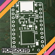
The Schematic with custom PMIC

This is my third revision PCB Schematic, last versions were using NICENANO v2 internals which are really outdated to this time.
This is the current Wafer schematic: the main MCU is an nRF52840 module (ISP1807) for low-power BLE/USB and running ZMK/Zephyr, paired with an nPM1300 PMIC that handles USB-C charging for a 250mAh LiPo, fuel gauging, and multiple regulated power rails for the rest of the board. The keyboard uses a Matrix and will feature 36 key layout, plus USB ESD/TVS protection, SWD Tag connect for JLink flashing custom bootloader for debugging, reset/soft-off controls, a status LED, and a connector for a small display (nice!view-style).
I also switched from a traditional power switch to a MCU-controlled soft-off button so the battery can keep charging at all times while still letting me fully use the soft-off feature; this will be implemented as a small side-mounted push button
Sasha
submitted Wafer Split Keyboard for ship review ago
Sasha
started Wafer Split Keyboard ago
12/13/2025 3 PM - The Schematic with custom PMIC
This is my third revision PCB Schematic, last versions were using NICENANO v2 internals which are really outdated to this time.
This is the current Wafer schematic: the main MCU is an nRF52840 module (ISP1807) for low-power BLE/USB and running ZMK/Zephyr, paired with an nPM1300 PMIC that handles USB-C charging for a 250mAh LiPo, fuel gauging, and multiple regulated power rails for the rest of the board. The keyboard uses a Matrix and will feature 36 key layout, plus USB ESD/TVS protection, SWD Tag connect for JLink flashing custom bootloader for debugging, reset/soft-off controls, a status LED, and a connector for a small display (nice!view-style).
I also switched from a traditional power switch to a MCU-controlled soft-off button so the battery can keep charging at all times while still letting me fully use the soft-off feature; this will be implemented as a small side-mounted push button
12/13/2025 4:16 PM - Firmware with ZMK and Zephyr modules
I modified ZMK for Wafer so the battery percentage comes straight from the nPM1300 PMIC, instead of relying on the usual “battery sensor” path: I added a dedicated battery reporting mode where ZMK talks to the PMIC over I²C, triggers a VBAT ADC measurement by writing to the nPM1300 “task” register, waits briefly for the conversion, then reads back the ADC result from the PMIC registers (MSB/LSB), reconstructs the raw value, converts it to millivolts, and finally feeds that into ZMK’s normal mV → % LiPo curve so the charge level shows up consistently in the UI/widgets and everywhere ZMK reports battery. I implemented this before the official ZMK 4.1 release, but on the same 4.1 codebase, so it stays easy to rebase and keep upstream-compatible.
I'm going to implement this solution for others, and merge changes to ZMK main soon
12/13/2025 4:24 PM - Soldering the PCBs
Part of the board (the charger section and most of the tiny SMD passives) was assembled at the factory via PCBA, but I still had to hand-solder the “hard” parts myself, the PG1316S ultra-thin switches and the ISP1807 module. Doing that by hand was honestly tougher than I expected because of the fine pitch, precise alignment, and the amount of manual work involved, but in the end everything seated properly and the board came to life. As a finishing touch, I also made antenna-area covers with my logo using AMS multi-material printing
12/13/2025 4:36 PM - CNC Milled Cases
The Wafer case is the most “mechanical” part of the project: an ultra-thin CNC-machined aluminum enclosure where the top piece acts like a clean frame/plate with cutouts for the PG1316S switches, and the bottom piece is a tight pocket for the electronics with dedicated space for the battery/magnets and all the openings for USB-C and the side soft-off button. I spent a lot of time dialing in the CAD so everything fits within a few millimeters and still feels solid and seamless — but real manufacturing can sometimes “mess up” even with good drawings: tool wear, fixturing/baseline shifts, tolerance stackups, or finishing (like blasting/anodizing) can push critical dimensions out of spec. That’s basically what happened on my first run, so it’s just another iteration: verify the problem areas, tighten the tolerances/inspection points, adjust the model if needed, and re-order to get the case to the level I originally designed it for.
12/13/2025 4:41 PM - Some Photos
I’m at the very last stage of Wafer, but I’m currently a bit stuck while I iterate on the case design and dial with a better manufacturing than JLCCNC. The electronics are working, now it’s all about getting the enclosure to fit and feel exactly the way I designed it. In the meantime, here are a few photos I managed to take along the way
12/16/2025 2 AM - Ergogen (March 2025): Just not another split
So from this point, I would journal and show everything I did to make Wafer (at least from what I remember)
I didn't have any plan at all, I just had that itch: "I want my own board with stagger". Back then I'd already built a third split and finally wireless low-profile Corne a few months ago, so I wasn't new to split keyboards... but PCBs were like a rabbit hole to me. I knew how to print, solder, flash my own ZMK config, But how about designing the boards itself? Eww...
So I just outlined my hand and sketched my first concept, and i remember thinking: "Hey that's hella nice!".
At this point i already knew that I want to 36 keys, the perfect for minimalistic keyboard that I got used to.
Then I discovered Ergogen, and it felt like cheating (in a good way)
First concept, i still like the personality of this of this outline shape
Thanks to the Ben Wallack video I found Ergogen: basically a programmable way to design keyboard layouts that can output KiCad files. For me as a beginner, that sounded so unreal.
The moment of the "ultra-thin" idea
While I was playing with layouts, something kept bothering me, something that I have seen in all DIY builds (including my own)
Devboards take an unnecessary amount of space. And it still looks unserious.
The stack usually ends up like: shield PCB, battery, devboard, display…
It works, it’s easy, but why am I wasting so much volume just because of the MCU pin headers, while I still have relatively small battery?
I wanted to get rid of this Sandwich as much as I could, I want a keyboard that is clean, with no "good enough" compromise
If the devboard is the reason the build is thick, why not to place the components on the shield? (and make a cutout for the battery)
It is a really simple idea, absolutely not new to any manufacturing but to that time I barely seen any split keyboard with it so far...
Maybe I should have a look at something else than reddit lol.
first wafer outline
12/16/2025 4 AM - “I’ll just borrow Mikoto…” (and learn the Right way)
I started with the most beginner move possible, zero knowledge, peak confidence.
My plan was simple:
- take the Mikoto MCU layout,
- "borrow" this schematic,
- add a nice!view display
- add a basic keyboard matrix learned from Joe Scotto video
- and jump straight into routing
From here I also decided to use a soft-off button instead of physical battery switch, this decision was actually decent
Mikoto is the open-source ready to jlcpcb production devboard
There was one tiny catch though: Mikoto is basically a bare MCU. And "bare" means: you are responsible for all painful stuff, decoupling, routing near the nrf52840... and scariest part: the antenna.
Think I accounted that?
keep thinking.
Layouting the first in my life PCB took me almost 3 weeks, and before I even went to place the components, I'd have to fix all of my board outline
first layout of Wafer
Of course I later figured out that this will obviously wont work well
some of my beginner mistakes:
this is a 6-layer PCB, and my routing still scares me.
I guess I was trying to add extra capacitance or what?
I picked a completely random 2.4 GHz antenna footprint and hoped it would work.
later I remade this board 2 more times from scratch.
Don't be like me.
12/16/2025 5 AM - Prototyping a case for Wafer
How the thinnest keyboard could be without a fancy case?
Right after my first PCB layout, I had one question:
How thin can this keyboard actually be… in real life?
So I teamed up with a friend from my makerspace who knew the Fusion, and we started quick case prototyping, just to test the shape and vibe. I wished to have infused stands, so the screws would be visible only from the bottom.
Of course the first prints were... humbling,
we made the display enclosure on a case smaller than the display itself lol.
We didn’t notice for almost a week, because the 3D model we used (nice!view breakout) was way smaller than the real PCB
Then we hit the next issue, electronics are taking a plenty of space.
They don't just take area, they take height. So we had to redesign cutouts and internal pockets way more aggressively than we thought.
And since my Corne already had that “snap together” feel, we decided to add flat round magnets too
However, despite all the early mistakes, we got 5mm on the thinnest part and 8mm in a display area. It was actually really thin
Later we squeezed it even more and pushed the thinnest section down to ~4 mm.
12/24/2025 5:03 AM - Ordering from China (Kailh, displays, magnets)
Once, Wafer stopped being a "layout experiment" and started becoming a real project, I'd have to think about important yet-critical part, ordering components.
Switches were the big one. Instead of buying a small batch from a Keycapsss store, I decided to do it properly and order directly from Kailh, generally to save and get lighter springs.
Basically there are a few versions of PG1316 available.
PG1316s is the classic ultra-thin SMD laptop switch.
PG1316c is slightly heavier and have a hot-swap support,
currently I made a footprint for them, but haven't tested them yet, they will be available soon with Wafer
PG1316m is a smaller format switch, usually used in a top row of the normal sized keyboards, like a 0.5U switch
The real quote:
PG1316S: $0.42/pc @ 500, with price breaks at $0.37 @ 1000 and $0.34 @ 3000
Keycaps: $0.08/pc
For comparison the prices from the shop:
PG1316s: $0,75 per one + $0.45 for keycap
Around the same time, I was also collecting the “Wafer essentials” from China:
displays (Nice!view off brand) and MagSafe-style magnets (so the halves snap together like they belong), all came out much cheaper than in regular shop:
Nice View module ~$10 Per piece
Magsafe magnets are really cheap, N52 are impossible to find in Germany with this thickness, costed me $3 for 10 pts.
12/24/2025 5:42 AM - New revision, saying goodbye to the "bare MCU"
After my early “Mikoto-style bare MCU” experiments, I finally accepted the obvious: a naked nRF52840 is not beginner-friendly, and it’s especially not friendly when you’re trying to build something ultra-thin.
So for the next Wafer revision i switched to ISP1807, an NRF52840 system-in-package module that already involves all MCU required schematic, even built in antenna inside of 8x8x1mm BGA.
In other words: instead of spending weeks guessing if my wrong impedance control is secretly sabotaging everything, I could focus on what actually needed. Power, matrix, and whole thin-stack design.
I also designed a 13 pin out, mostly to save on via-in-pads and make the routing easier.
The charger is being the same for now, later I will explain why I moved to a better ones.
Footprint evolution: PG1316S, custom tweaks
Another big change in this revision was the switch footprint.
Old footprint:
New footprint:
I changed the contact pads bigger for easier soldering, so there is less chance of cold joints or “barely touching” pads.
12/24/2025 11 PM - From “nice!nano combo” (BQ24075 + MAX17048) to nPM1100
Early Wafer power was basically the classic nice!nano-style setup, a simple charger, plus a BQ24075 and a MAX17048 (because I really wanted proper battery percentage).
Then the obvious question hit me: why im not using a proper PMIC?
The nice!nano power layout is optimized for mass production, and it is a charger straight from 2008. For Wafer, the difference of a couple dollars in BOM cost didn’t matter, but efficiency and integration did
Also… no way I was going to stick with an LDO-only approach if I’m trying to squeeze every millimeter and every percent of battery life
Meet the NPM1100
a tiny Nordic PMIC with an integrated charger and a DC-DC regulator
So what I've got:
Fewer parts -> fewer routing traps -> more space for the layout.
USB charging support with auto port detection
Ship mode for a true off state
and best thing: A proper buck regulator instead of wasting energy in an LDO
Going from ~78% to ~92% efficiency is basically free battery life, almost a 20% gain just from not burning power as heat.
The only tradeoff is that nPM1100 up to 400 mA, not 1.5 A like BQ24075, but for my tiny battery it doesn't matter at all
12/25/2025 12 AM - Designing the Wafer logo
From the beginning I wanted to create a font-based logo that feels like the keyboard itself: soft corners, chunky geometry, and slightly playful.
I started in Figma with a blocky font as a quick placeholder. It looked expressive and I really liked the vibe, but readability was terrible. So I began reshaping every letter manually, aiming for something closer to the picture I had in my head.
The first logo iteration
The trick that made everything “click” was superellipses (aka squircles).
They’re everywhere in modern type and logos, but you would never know about that.
It gave me the exact vibe I wanted, and still recognizable even at tiny sizes.
build a logo system, not just a logo
I made multiple versions for different use cases:
A big inspiration here was Totem PCB aesthetics silkscreen
Then I pushed it further and made the final design I actually used on the keyboard.
I love how it turns the back of the keyboard into an artifact that you discover only after unscrewing it, like a hidden spec sheet / lab label.
It has a tiny details you can stare at for really long... and thats exactly the point.
12/25/2025 2 AM - Wafer V3: final power design with nPM1300
After the BQ24075 + MAX17048 version and the intermediate nPM1100 idea, I finally got to what I actually wanted, a proper PMIC that handles charging + power rails + battery telemetry all together, and it lets me control all over I2C.
On this Wafer revision the power "heart" is now the Nordic nPM1300, basically an upgraded nPM1100. It replaced a big chunk of my previous circuitry and gave me a lot of control with the software. I used to require a separate fuel gauge and a lot of extra hardware.
Some of the nPM1300 characteristics:
Two buck converters, one of them is up to 2.7v, and second 3.0v, I chose the second one to have a good compatibility with nice!view display
Two LDO or two load switches, basically configurable via software, and make to control all the external devices, I put a display here, so I can turn off with ZMK's external power
Configurable charger, lets you precisely control the charging, current, cut voltage, discharge, thermal monitoring and a lot more, I also implemented a custom virtual fuel gauge for Wafer. Charging current is configurable from 32mA up to 800mA through DTS config nodes.
Here is my schematic for PMIC
They also advertise the "fuel gauge" inside,but it’s basically a software estimator that relies on sensor values + a pre-programmed battery profile. To make it accurate, you need Nordic’s battery profiling workflow + dedicated dev kit, but for my use case it didn't really make sense. So I moved with my own approach.
I also made a production-ready PCB variant
For this revision, I created a panelized version with mousebites. Instead of sending two completely separate PCBs, both halves are connected with breakaway tabs (with drilled perforations).
12/25/2025 3 AM - The Firmware, how I implemented custom board with ZMK 4.1
Earlier, I already made a custom wafer shield, back then it was just a nice nano board with custom kscan layout.
I ended up maintaining two repos at once:
wafer-zmk-config is the board config with defs, keymaps, overlays, DTS settings and display C files, and a lot of why is this build failing again?.
my ZMK fork, a Pete Johansson fork that became my base before the official Zephyr 4.1 release, where I had to change ZMK code because Wafer hasn't standard components.
The battery rabbit hole: I needed a battery percentage to show up
Because Wafer uses the nPM1300, I wanted battery reporting that doesn’t rely on a separate “battery device” or an external ADC divider. So I added a new battery fetch mode that reads VBAT directly from the PMIC over I2C
In my ZMK fork, I introduced a new Kconfig option
ZMK_BATTERY_REPORTING_FETCH_MODE_NPM1300_DIRECT (nPM1300 VBAT direct read)
What I changed in battery.c (and why)
1. New fetch mode path
If my config direct mode is enabled, ZMK doesn't try to fetch a battery device, instead it calls my function zmk_npm1300_read_vbat_mv(&mv) and then maps it to % with the existing helper.
2. I kept the logic as it was
I kept the existing approximation, that's already good enough to show the percentage
The core hack npm1300_vbat.c
This file is basically talks to nPM1300 ADC registers
How it works:
- Its using the devicetree PMIC node
DT_NODELABEL(pmic)and grabs the i2c spec from it. - Selects ADC bank
0x05and triggers VBAT measure by writing[bank=0x05, reg=TASKVBATMEASURE(0x00), value=0x01] - Waits a bit of time (Just for safe margin)
- It reads the ADC result over registers MSB and LSB bits separately;
- it combines the results and converts them to millivolts (in the range of 0mV to 5000mV).
Also later I plan to make a custom soft off module so either power button will turn off both of the keeb halves
1/15/2026 3:10 AM - Wafer case, how CNC became an another project, Part 1
When I started the Wafer case, it became absolutely obvious very quickly, this won't be "a box around pcb", and since my goal is CNC aluminum, my whole process became into a chain of decisions where every choice affects the next one.
Since start of the case model, I made 30+ revisions that I 3D printed before I managed to make the first order.
renders of the one of the first iteration of the cases that I posted on ZMK Discord
Basically, the difference between designing part for 3D printing is really simple. 3D printer adds the material, CNC cuts the material out, so your not just drawing a shape, you're mostly preparing a manufacturing process, the geometry with CNC is inseparable from tooling and fixturing.
Fusion has a free CNC simulation tool to prepare the model that helped a lot with understanding how the model will be cut
At the start I had a few zones that I designed for:
- the display (and its real dimension, not only 3D model)
- PCB, battery and a bit of wiring
- magnets/ and how halves snap together for travel
- the soft-off switch access
- screws, bosses and overall look
Princip: make the stack work first
When I started designing I started a version where everything is at least fits and assembles, it was all 3d printed, but back then that is a great way to try fit the components that you already had.
This this the first revision of that case, here I already decided to make the model sloped to preserve the thickness, but the standoff are looking pretty weak and lonely now. I wanted to integrate standoffs to get the screws only on the bottom.
1/15/2026 3:33 AM - Wafer case Part 2, fitting everything for CNC
After first "stack-fit" prototypes, where the goal was only PCB + Battery + Display = Physically possible to assemble, I started to shift the cases from shape design, into the feature design.
These are the evolution of the revisions im making, my principle is to add the thickness back to my design, to shape it perfectly to the CNC-ready model.
The new display cutout
The underneath is being much solid now that it was
And another display work to get it to the final shape
The antenna cutout remained the same here, despite I changed it for ISP1807 RF requirements later
1/15/2026 4 AM - Wafer case Part 3, prepare the model for new wafer layout
The big visible change here is the display pocket + RF cutout, as I don't need to waste so much space to the bare mcu anymore, now im having a tiny SOC instead!
Also, I've increased the size of the standoffs here to match the requirements later.
Bottom cases
Despite I have only shown the top cases as the changes, the bottom also had quite few changes
Added the magsafe magnets to the case