ES_01 E-ink Smartwatch
A 5mm thick smartwatch which achieves its thinness by laying out each of its components in a straight line, in their own modules which can bend around each other to conform to the wearer's wrist. The watch features a main E-ink touch display that consumes very little power, accompanied by two small OLEDs at the top and bottom to show rapidly changing data (Like seconds, heart rate etc.). The watch incorporates an ESP32-S3 microcontroller for main processing and establishing a Bluetooth connection to a smartphone. It also incorporates heart rate sensing, an intelligent inertial measurement unit and a pressure/temperature sensor to provide rough fitness and altitude tracking as well.
Created by
 sandgum
Tier 1
3711 views
82 followers
sandgum
added to the journal ago
TROUBLESHOOTING and... Announcement of PCB Version 2!
Hi!!! Sorry for the radio silence, I’ve kinda been busy with exams at school. Anyways, I have made some progress on the ES01, which is now going to be unofficially called the ES01.1 (More on that later)! The ESP32-S3FH4R2 chip finally arrived, and I quickly desoldered it from its devboard and reflowed it on the ES_01’s PCB… and then it didn’t enumerate on USB. The whole board was drawing a stable 34mA when idling, but USB enumeration still failed. To combat this, I spent around 5 hours at the hotplate reflowing the board again and again, but still there wasn’t any result.
WHY must this happen? Alas, it is just a part of electronics design for your hard work to fail in front of you. Eventually I figured out the problem, and that is that my flex PCB was flexing way too much. It kept bending when at high temperatures, which made it so the ESP32’s pins did not actually connect to their respective pads. Even when they did connect, the solder joint was too weak and not solid enough for proper USB enumeration to start. Moreover, I did not add any other ways to flash firmware onto the chip apart from USB, and constantly soldering and desoldering programming wires was way too cumbersome and could cause further signal integrity loss. Using a flex PCB and not having more breakout points was a major error.

pretty much no breakouts of any GPIOs...
Another major error was the PCB’c connection to the E-ink display, as I must’ve misunderstood technical drawings and placed the display’s two connectors in such a way that the display was flipped! This shouldn’t affect prototyping, but prototyping is already hindered by the ESP32 chip’s faulty connections.
I have also realised that going for a flex PCB was another major mistake, as it significantly increased the cost of the watch, and constant bending of a 4-layer PCB during daily wear would almost definitely cause fatigue that can break traces.
It is for all of these reasons that I have decided to completely redesign the ES01’s PCB! This “ES01.1” PCB will be rigid (so it will be MUCH cheaper), it will use pretty much the same components (so I don’t have to buy them again), but address the major flaws in the last design.

This isn't the exact model, but you know what I mean, it's basically like the connectors inside phones
Firstly, the PCB will feature a tiny smartphone-style connector that will be used for USB programming, so no more soldering and desoldering wires. The board-to-board connector will connect to another programming board with a USB-C connector, so I don’t even have to cut up cables just for this project.
Secondly, the PCB will have much thicker internal copper (as it will be rigid), and it will also be split up into 3 parts. These parts will be connected together with hand-soldered wires instead of a flexible PCB, and that means that this should be far more durable than its predecessor.
Finally, I will optimise the routing of every trace by changing the component placement, so this PCB will truly be completely revamped. I was not happy last time with my 3.3V power distribution traces, as they were likely too thin to support the power spikes of the ESP32-S3, and could probably cause a significant amount of electromagnetic noise that affects all the signals. Also, having both OLEDs, the IMU, the hard rate sensor, the E-ink touch controller, the pressure sensor, the haptic driver and the battery fuel gauge all run from the SAME I2C line most likely would have resulted in significant problems such as lag, bus saturation and devices fighting over each other. Accounting for this was also very weird in the firmware, with the heavy use of I2C semaphores in every driver. The ES_01.1 PCB will use at least 2 separate I2C buses for groups of sensors, such as a separate bus for displays, and a separate one for sensors.
Lastly, the debug connector in the ES_01.1 will also expose UART, JTAG and a couple of GPIOs that will be broken out on the same USB-C board for failsafe programming.
There will be some implications to this redesign. It will mean that I have to redesign some parts of the enclosure, and also it will make the whole PCB much thicker than the 0.2mm flex PCB, although I can just option the thinnest 4-layer rigid PCB from JLCPCB. This PCB is also outside of my allocated Blueprint budget, but that’s completely fine, as I will find the PCB myself (It’s not that expensive, after all).
Stay tuned for the PCB design process (2.0)!!!
 6mudahad
gave kudos to ES_01 E-ink Smartwatch ago
6mudahad
gave kudos to ES_01 E-ink Smartwatch ago
Wooooow, this is amazing!
6mudahad
gave kudos to ES_01 E-ink Smartwatch ago
Wooooow, this is amazing!
 Duckers
gave kudos to ES_01 E-ink Smartwatch ago
Duckers
gave kudos to ES_01 E-ink Smartwatch ago
This is so cool! Make 2....
sandgum
added to the journal ago
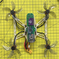
Assembled PCB, Troubleshooting
After receiving the PCB for ES_01, I immediately began work on assembling it.
First, I started with taping the actual PCB to my workspace, after which I precisely aligned the solder stencil with the gold pads on the PCB.
Using an old ruler as a squeegee, I spread solder paste over the stencil, and made sure that every pad was covered with just the right amount of solder past while ensuring that none leaked out.
After this, it was time to place each component on its respective pad. The main ICs were relatively straightforward to place, but the tiny 0402 sized resistors and capacitors were right at the limit of what could be manipulated with my tweezers. For more precise placement, I used a small sewing needle to push each component to exactly where it needed to be. A lifesaving design decision I made when creating the PCB was to use hand-solderable pads for all my 0402 components, which have much more area so it’s easier to place components by hand. Ideally, if the ES_01 were to be mass manufactured, it would need a pick-and-place machine to do this task with a higher precision.

During placing these parts, I encountered a problem with one of the packages I ordered. The MAX17048 Fuel Gauge IC which was supposed to be in a relatively small QFN package actually came in a ridiculously small BGA package. I’ll update the electronics BOM to reflect this mistake. After placing all the components, I brought the PCB to my reflow hotplate, where the solder melted and joined pretty much all the pads to the right pins with the exception of some pads on the ESP32-S3 chip and the tiny LGA pads on the Bosch BHI260AP. The solder bridges between these pads were easily solved by removing the chips while the solder was still molten, and using a small soldering iron to wick away some of the excess solder, after which the chips were placed back onto their pads.
Lastly, I cut up an old USB cable and wired the data and power connections to their respective pads on the PCB. These are effectively debug and firmware flashing pads.

After TRIPLE-CHECKING all the connections were perfect on the PCB, I finally decided to plug the board into my PC. A great sign was that there was no magic smoke or burnt components anywhere. And a USB connection was even being initialised! This, however, didn’t work out, and Windows kept telling me that my device was malfunctioning.
Now came the troubleshooting. I theorised that the ESP32 chip was booting up, but the USB connection was failing because the 3.3V rail took too long to reach its voltage upon being plugged into USB power. I connected my multimeter to the rail, and it took roughly 0.3-0.4 seconds for the rail to stabilise, and this might have been too late as the USB connection starts communication almost immediately. The voltage mismatch between the board’s 3.3V rail and the USB’s 3.3V signals might have been enough to disrupt the connection.
To confirm this, I wired the 3.3V rail to a clean 3.3V source from my bench power supply, and the board was consuming a steady 17mA, which was promising. This confirmed that the ESP32-S3 was alive and well. However, I plugged in the USB, and again, the same problem emerged.
At this point, I pretty much had no other leads as to why this USB connection issue was happening, until I took a closer look at the schematic for the ESP32-S3 ZERO dev board I based my schematic around. Despite their same appearance and apparent microcontroller cores, the dev board used a specific model of the ESP32-S3 with built in SPI flash in the package. The “plain” ESP32-S3 chip I had ordered did not come with ANY flash, and needs external SPI flash to even boot up and connect to USB!

Through an incredible stroke of luck, however, the ESP32-S3FH4R2 (the model I was supposed to use) is exactly pin-compatible with the regular ESP32-S3, and can simply slot into the same place the old chip was in. This should provide around 4MB of flash memory to actually store programs, and the ESP32-S3 should initiate USB communication with the PC now. The only thing left was to actually get the chip…

To avoid the expensive shipping fees (and long wait times) from vendors like DigiKey and LCSC, I resorted to buying an actual ESP32-S3 ZERO dev board from AliExpress, which I plan to harvest its chip from to put into the ES_01. It should arrive around the 16th of March, so it’s much faster than the other vendors I mentioned before. See you then!
 Anicetus 🚀
gave kudos to ES_01 E-ink Smartwatch ago
Anicetus 🚀
gave kudos to ES_01 E-ink Smartwatch ago
this is absolutely insane. awesome job
 Tomas Kuchta
gave kudos to ES_01 E-ink Smartwatch ago
Tomas Kuchta
gave kudos to ES_01 E-ink Smartwatch ago
I'm so excited to se the PCBs arriving 🛬. 🔥 Can't wait for the finished product 😃
sandgum
added to the journal ago
PCB has arrived!!!
All of the parts from JLC have arrived! This includes the all-important main flex PCB, the solder stencil for it, and the one metal 3D-printed part meant for cooling the really hot ESP32-S3 chip!

The PCBs turned out basically flawless, with them having just the right rigidity in the parts with stiffeners, and just the right amount of flexibility in the parts that bend. It’s only now that I realise how crazy small the components in the ES_01 really are, but I’m reassured because now I have a proper stencil.

The stencil is really huge compared to the PCB it’s for, and I guess I’ll frame it and hang it up in my room after I don’t need it anymore! There is a small problem with the metal 3D printed part though.

It is quite warped, and I was notified of this issue by JLCPCB, but I insisted that they manufacture the part. This isn’t that big of a deal however, as since the part is made from steel, I can heat it up on a hotplate and bend it back into shape if I’m careful. Otherwise, this haul from JLCPCB was successful, and I look forward to assembling the PCB of the ES_01!!!
 Dhruv
gave kudos to ES_01 E-ink Smartwatch ago
Dhruv
gave kudos to ES_01 E-ink Smartwatch ago
This is peak, oh my days.
 anshum.2422
gave kudos to ES_01 E-ink Smartwatch ago
anshum.2422
gave kudos to ES_01 E-ink Smartwatch ago
Soo great watch
sandgum
added to the journal ago
Reworked Trios UI, added Timetable app, and parts arrived!
Sorry for being silent for a while, cause these parts are do take their time! Anyways, this journal entry is an update on what has been happening in the past two-ish weeks, and BOY do I have some updates to give.
I continued with the firmware development process of the ES_01, with a bunch of newly-added functions which I still had to actually develop. But before I did that, I started reworking the internals of the UI which Trios (Yes, I came up with a name for the firmware) runs on.
Looking back at my EEZ Studio project, especially the timekeeping app could have a bunch of its logic offloaded to EEZ Flow instead of implementing it in Trios core (the main ESP-IDF project). Both the stopwatch and timer features can be implemented in the EEZ Flow engine, so that’s exactly what I did, and it works!!


Ignore the blue lines, those are just flow logic arrows which won't be visible while running
After that, I started with redoing the notifications section in Trios. Before, Trios could only store a maximum of 32 notifications at a time, and ALL of them were loaded into the ES01’s RAM on startup. Since strings take up a LOT of data, this would both eat RAM and restrict the number of notifications users can see. This was unacceptable, so I reworked it so that only 4 notifications are loaded into RAM at a time, and Trios will get any other notifications from the ES01’s internal flash that can store WAY more data. Of course, implementing actual flash file storing logic is beyond the scope of the UI, so I just let the UI call some functions which I’ll define in Trios core later.

The third thing I added in Trios’s UI was the timetable app. This app shows upcoming events for the whole week, and it will have its timetable events loaded onto it by the ES01’s iPhone app. To implement this, I created two rollers, one that scrolls through the events happening today, and another which scrolls through the days of the week, updating the first roller each time. Since a user can have an arbitrary number of timetable events, it would be terrible to have them all loaded into RAM for every day of the week, so only a single day’s events are actually in RAM. Trios will fetch the timetable events for each day from the ES01’s internal flash when they are requested by the user. Lastly, I created a timetable screen which flashes 5 minutes (or a configurable amount of time) before a timetable event to notify the user.


Apart from the progress I made on Trios, the first of the ordered components for the ES_01 finally arrived today, which includes the huge box of tiny SMD components ordered from LCSC electronics! The flex PCB should arrive within the next week, after which I can finally start assembling the electronics for the watch! Stay tuned for further updates!

 maslennikova-sofiya.s
gave kudos to ES_01 E-ink Smartwatch ago
maslennikova-sofiya.s
gave kudos to ES_01 E-ink Smartwatch ago
kudos
 kapoorritwik82
gave kudos to ES_01 E-ink Smartwatch ago
kapoorritwik82
gave kudos to ES_01 E-ink Smartwatch ago
absolute horology
 Joe
gave kudos to ES_01 E-ink Smartwatch ago
Joe
gave kudos to ES_01 E-ink Smartwatch ago
Dude. You have contributed to society. this is amazing, you are a net positive in the world.
 shaan 🚀
gave kudos to ES_01 E-ink Smartwatch ago
shaan 🚀
gave kudos to ES_01 E-ink Smartwatch ago
this is really freaking cool
sandgum
added to the journal ago
PARTS ORDERED!!!!
I FINALLY ORDERED THE PARTS!!! After like so much time meticulously looking over and refining the scariest parts of the ES_01 (namely, the PCB), I have activated my Hack Club grant and have ordered the majority of the parts from LCSC and AliExpress, and also the PCB and Metal 3D-printed E-ink bottom plate from JLC.
Firstly, just to make sure I wasn't going to order the wrong parts, I reloaded the Electronics_BOM.csv file from my repository onto LCSC, and good thing I did cause I found a couple of problems. There were 4 models of resistor in my BOM which were completely out of stock and backordered on LCSC, and they would've taken 60 DAYS to get back in stock (Yikes), so I quickly changed those resistors out for ones that were in stock.
Also, looking at my AliExpress cart, I found that the 401225 batteries I was going to usei in the ES_01 were not available anymore, but that wasn't a really big deal as there were like 20 other listings selling the same thing. However, looking at these listings, I found a battery which was almost the same size as the 401225 batteries I was going to use, but have 30mAh more capacity each.

These are 401230 batteries, with them being 30mm long instead of 25. After a quick check with my 3D model, I found that these batteries can easily fit into the battery compartments in the ES01, so I set out to work modifying those segments from the inside to fit the extra 5mm. That turned out successfully, and now the ES01 has a significant boost in battery capacity, going up from an already hefty (for a smartwatch) 300mAh to just under 390mAh! For comparison, this is roughly 50% MORE capacity than an Apple Watch (non-Ultra), which uses a much more power-hungry S-series chip and OLED panel, so the ES_01 should now last ridiculously long, even with its ESP32-S3 chip.
As of now, I have still yet to order some random very specific connector (from Alibaba) for my OLED displays to work, but those only cost like $7. I've also gotten 3D-printing arranged as well (Shoutout to 0x62)!!!
sandgum
added to the journal ago
Final FINAL finishing touches to 3D model and new "apps"!
It’s time to make the FINAL FINAL finishing touches to all aspects of the ES01’s hardware, and what was left to refine was the actual 3D model. This whole time, the ES01 had no actual logos or identifiers on its 3D model, which I saw as a MASSIVE oversight that I promptly fixed. I installed the same Doto font from Google Fonts that was used in the main title screen of the UI, and cut away a nicely-proportioned “ES_01” in the top of one of the battery segments. Since that part of the top battery segment was only around 0.2mm thick, the indents of the text became holes which will show the real colour of the battery underneath. I think that’s actually pretty cool.

Next to the ES_01 branding, on the second battery module, I put an embossed piece of text saying “Made in Australia” and rotated it by 180 degrees (hehe!). On the other side of the watch, the Triangulate logo and name were also embossed on the haptic driver segment of the watch. These texts only rise 0.1mm above the surface, so they are pretty subtle and not overly “in your face”, which would ruin the clean aesthetic. I also made a minor change to the display segments by rounding in the “cliffs” between the 3D-printed top cases and display screens for easier touch-ability, especially on the main panel.

One more BIG change I made to the ES_01 is in its side TPU pieces, which now introduce a 60° downwards angle between the main E-ink segments and the OLED segments. I decided to do this because when worn, the angle between the E-ink and OLED segments are going to be quite large, (as you can see in the renders with a hand), and having a TPU piece that bends THAT much will pretty much guarantee failure in the future, That's why I rebuilt those pieces from scratch to account for that angle, and now the TPU pieces will not bend nearly as much when worn.

I also made some changes to the UI after gaining a bunch of new ideas for functions the watch should do. As I recently started Year 12 of school, I found myself wanting to have my timetable on my watch so that I don’t have to access my phone (only for it to be confiscated). Then I noticed my smartwatch, and most smartwatches, for the matter, didn’t have a feature for this. This is why I created another page in the main menu in the UI, and added 4 MORE “apps” (just concepts, not developed yet) that I think would be really useful for a lot of people, whether they are in school or not. First is the Timetable “app”, which stores all your timetable data and displays it to you, as well as keeping track of time and telling you which class or meeting you have next through notifications. As it’s pretty complicated to set up each entry in ANY timetable, I have relegated the actual timetable editing to the iPhone app. So users can edit timetables and calendars in the app, and just observe them through the watch.

Which brings me onto the next “app” I added, a Calendar. This basically functions the exact same as the Timetable “app”, but instead does not repeat and is meant for one-off events. Next, I added a “Find ur Phone” button in the main menu, which, through the app, causes the user’s phone to vibrate and make noise so that they can find it. It would have also been nice to include an Ultra Wideband module which works with Apple’s Find My so that users can locate their phone with more precision, but I guess that’s something to implement in version 2!

Lastly, I added a Shot Button to the main menu, which, when tapped, triggers the user’s phone to take a photo. This feature is similar to one found in Apple Watches, and it allows the user to set their phone down and remotely trigger a photo while they’re standing in front of it.
Now that the 3D model of the ES_01 is completely refined as well, I think it’s now FINALLY FINALLY time to order the parts!
 Cubic-Vyper
gave kudos to ES_01 E-ink Smartwatch ago
Cubic-Vyper
gave kudos to ES_01 E-ink Smartwatch ago
This is amazing
 Moses Shriver
gave kudos to ES_01 E-ink Smartwatch ago
Moses Shriver
gave kudos to ES_01 E-ink Smartwatch ago
Damn bro, that’s insane!
 kwanyeung.chow1 🚀
gave kudos to ES_01 E-ink Smartwatch ago
kwanyeung.chow1 🚀
gave kudos to ES_01 E-ink Smartwatch ago
this is amazing
 issofc657
gave kudos to ES_01 E-ink Smartwatch ago
issofc657
gave kudos to ES_01 E-ink Smartwatch ago
wow that's so cool
sandgum
added to the journal ago
Fixed PCB Errors and added Fuel Gauge chip
As I recently got my grant from Blueprint (Finally!!!), I can now start work on actually ordering the hardware that will make the ES_01 come to life. But first, I had to check all of my PCB documents to make ABSOLUTELY sure that my PCB was wired and arranged correctly, and I'm glad that I did do that.

Looking at my schematic, I found that the circuit for the main E-ink display was wired wrong enough that the PCB would not work at all if it was manufactured with that defect. After correcting the errors in the E-ink display circuit so that it matched the application circuit in the datasheet, I also found out that the connections to the touch panel for the E-ink display were wired in the wrong order. As the cables from the E-ink display have to bend around to reach the connectors on the PCB, the physical contacts are reversed, which I hadn't accounted for when wiring the touch panel's connector. Thankfully, that was also a quick fix. These schematic modifications did not result in major changes in the PCB layout either, so it was all done quite quickly.

I also made another modification to the schematic, which involved adding new components entirely. Specifically, I wanted added a MAX17048 fuel gauge chip which can measure the voltage and also calculate the amount of energy flowing through the batteries in the watch to provide an accurate estimate of the battery percentage. This is very similar to chips used in phones and laptops, and crucially allows for the watch to put itself in deep sleep when the battery gets to a low enough percentage so as to not damage the cells. I chose this specific chip mostly because it's extremely small and widely supported by the ESP32 community, so I won't have to write any sketchy drivers for it.

Because the chip is so small, it was able to fit easily in the less dense parts of the flex PCB which are underneath the OLED panels. Plus, the fuel gauge communicated via I2C, so those lines were easily connected to the same lines used to drive the OLEDs.

Now all that is left is to actually order the parts!
sandgum
added to the journal ago
Activity, Vitals, Notifications, Timekeeping, Weather apps!
Ok, I have been HARD at work relentlessly trying to complete this UI, because I have created 7 of the 8 "apps" that form all of the functions that the ES01 is capable of. The first of the "apps" created during this time is the Activity "app", where it provides the user with all the information regarding step count, exercise time and total calories burned during the day. The Activity "app" has easy-to-read arcs which visualise the total percentage of each of the three tasks, which all get their data from the watch's sensors and user actions. The number of steps, exercise goal and calorie goals can also be adjusted by the user, and all of the visualisers in the Activity "app" reflect those changes. Much like most of the "apps" in the ES01's UI (Which I have named es_OS), the Activity "app" has two pages, with the other page showing a zoomable graph of each of the activity parameters. This allows users to see trends in their performance and activity levels, with a button cycling through all three parameters at the bottom.


Next up was the design of the Vitals "app", which provides real-time data from the MAX30102 sensor in the watch. This "app" is very similar in layout to the previously-designed Altimeter "app", with there being a dedicated page for heart rate and blood oxygen levels, with each page showing current values as well as zoomable graphs.


After this, I decided to tackle the challenge of implementing a proper way for users to receive and view notifications, which started with a "pop-up" notification page. This page is shown by ESP-IDF whenever there is a new notification, with the page showing a maximum of 9 lines of text to show as much of the notification's content as possible. Since this page will interrupt users wherever they are in the UI, I created a much larger-than-normal back button for users to immediately find and hit to avoid annoyance. After this, I created the main Notifications "app", where the user can scroll through pages of their past notifications. Now, I could create a bunch of different pages depending on how many notifications there are, but you have to define each page in EEZ studio beforehand, and also it would make the code extremely unreadable and clunky to have a TON of pages. This is why I chose to give the user an illusion of switching pages, when in fact they are only switching the text in one page. This makes the generated EEZ code much more decipherable (in the very likely event I forgot to add some logic) and is just elegant in general. Plus, the pop-up notifications page is also used to view any of the notifications in the Notifications "app" by clicking on them.

Ignore the blue lines, those aren't in the final UI

After creating the UI for that, I moved on to making the Timekeeping "app", which houses a stopwatch and a configurable timer which continue in the background when the user leaves the "app". I decided to make these features look unique, yet still part of the UI, with the stopwatch page showing a large half-arc which shows seconds. The numbers displayed are large as well, and this page turned out to be one of my favourites for how simple yet elegant it subjectively looks. The timer page adjacent to the stopwatch shows LVGL UI elements that are new in this project: number rollers. Three number rollers allow for the user to pick seconds, minutes and hours, with a nice haptic tap happening when they change any of those values (iOS style!). Instead of having a separate label showing the actual timer's time, I also decided to use the number rollers themselves as labels, which saves a bunch of screen space and also makes the timer more user-friendly.


And lastly, I created the Weather "app" , which shows the user weather data which will hopefully be relayed to the watch from an iPhone with access to Apple's Weather API. This "app" consists of two pages yet again, with one showing the weather today, and the other showing the weather for the next 10 days. This first page shows the current temperature from the iPhone in huge letters, and also the temperature measured from the BMP585 sensor on the watch. Paired with that, the max and min temperatures are also shown, as well as the current weather conditions in the form of an icon. The right side of the page has a roller which shows the expected conditions and temperature for all of the hours of the day. The weather forecast page shows another roller which shows the weather for the next 10 days, and below that is a zoomable graph showing the temperature over those 10 days.

Yeah the icons look cooked, that's just because all of them are placed on top of each other. In the actual UI, only one of them is shown at a time

Over here, the Day roller actually has a really long bit of logic to actually display the day of the week, it looks normal once its running
This user interface is almost completely done now, with the only elements left to implement being the settings page where the user should have plenty of choices to customise the UI to their taste. I also still have to implement blood oxygen sensing algorithms in the main firmware, and also need to add BLE support to the firmware. But for now, I'll focus on the hardware to make this watch come to FRUITION!
 lamontjack202
gave kudos to ES_01 E-ink Smartwatch ago
lamontjack202
gave kudos to ES_01 E-ink Smartwatch ago
Looks so cool and modern, would genuinely love to build and wear this
 tap
gave kudos to ES_01 E-ink Smartwatch ago
tap
gave kudos to ES_01 E-ink Smartwatch ago
THIS SHIT IS GAS!
 Tanuki ⚡🚀
approved ES_01 E-ink Smartwatch ago
Tanuki ⚡🚀
approved ES_01 E-ink Smartwatch ago
Tier approved: 1
Grant approved: $258.00
Im sorry, did I give you a permit to cook? Why did you cook this hard? AMAZING PROJECT!!!!!!!
sandgum
added to the journal ago
Implemented Workout and Barometer "Apps" in UI
After creating the basis upon which the ES_01’s user interface will be built, including the all-important design and aesthetic direction I would be heading, it was time to flesh out the watch’s basic navigational UI (basically, how is the user going to get around the different “apps” and functions of the watch?).

unrelated, but cool render of the watch's enclosure (for the banner)

First of all, I have decided to go with an “apps” structure for how functions will be laid out in the watch, with each sensor reading or calculated value appearing in its own “app” complete with other relevant stats and numbers. This is quite similar to how many low-cost smartwatches structure their UIs, such as examples from Huawei. Higher-end watches like the Apple Watch and Samsung Galaxy watches use a more “phone-like” approach to their UIs, where most raw sensor numbers are calculated into insights or trends for the user to see. This, of course, introduces A LOT of computing overhead, which the beefy chips in those high-end watches can easily handle. The same cannot be said about the ESP32-S3 I am using.
So, I needed to create a “Home Screen” of apps on the ES_01, but I was significantly limited by the capabilities of the e-ink display I am using. Since even a fast refresh of that panel takes about 1.5 seconds, it would be INSANELY clunky for the user to be able to scroll through the various apps and menus in the UI. Plus, the goal with any E-ink display is to do as few refreshes as possible, because even though the panel consumes no power when its just sitting there, refreshing the panel consumes quite a lot and frequent refreshes can outweigh the power savings e-ink panels are known for. That’s why I decided on reserving the top of the watch’s screen EXCLUSIVELY for navigation buttons, like forward, back and switching between tabs.

Placing the navigation buttons in a consistent place, and always colouring them in white creates a sort of muscle memory for the user, very similar to how Android phones always have the back button on the bottom of the screen. I have also designed the placement of each back button in my UI to make it so that if a user keeps pressing the top-left corner of the screen repeatedly, they will always end up back at the watch face. Also, since my “Home Screen” only has two pages, it’s not that bad to navigate between them using buttons.
Most of the “apps” that I will develop for this watch will have more than one page, in which case I have settled for using a “tab switcher” element at the top to switch between two or more pages. This makes sure the user can switch between every page very easily, and doesn’t have to use back and forward buttons which they could easily get lost in the UI with.
Ok, Ok, enough about me blabbering about the UI’s actual design, let’s get to the two “apps” that I have implemented so far. First on the list is one of the most complicated “apps”, the Workout app. Clicking on its icon in the Home Screen takes you to the New screen, in which you can choose your workout to do right now, or you can switch to the Stats screen, which shows your workout activity in a zoomable graph, and your three favourite workouts plus how many times you did them.


Selecting a new workout takes you to the active workout page, which starts the workout (which will be a task in ESP_IDF) and shows you your total calories burned, pause and end buttons, and a HUGE button that maps to a counter which can count pretty much whatever you want. If you’re running or cycling, you can use it to count laps, or you can use it to count sets if you’re weight training. It’s super useful, and I haven’t really seen it implemented in any other watch. On this screen, you only see one stat. This is on purpose, as most of the workout data is shown on the OLEDs, as the data is rapidly changing. Calories only update like once every 10 seconds, so that’s fine to show on the E-ink display. I have specifically designed the buttons in the active workout page to be as large as possible, so they’re easy to press in the heat of the moment.


After pressing the End button, you are taken to a confirmation screen which asks you whether to actually end the workout, and if you press End, then you are taken to a workout summary page specific to the workout you just did. This shows a graph of either heart rate, calories, or distance/reps over time (By tapping the button that says “Tap”), and also shows average heart rate, calories and the total time spent in the workout.

That’s the workout “app” done, after which I moved onto creating the Barometer “app’s” UI. This consists of two pages, one showing the current altitude and stats relating to it (including a zoomable graph), and an identical page showing the same data about air pressure in hPa, which can be used to roughly forecast weather. I have also mapped the Altitude icon in the watch face to this app.


There we have it! The first two “apps” are fully fleshed out, and there are now six to go!
 CircuitGuy
gave kudos to ES_01 E-ink Smartwatch ago
CircuitGuy
gave kudos to ES_01 E-ink Smartwatch ago
Absolutely wild, this is super cool!!!!!
 Visage
gave kudos to ES_01 E-ink Smartwatch ago
Visage
gave kudos to ES_01 E-ink Smartwatch ago
Dayummm, this shit is firee!
 anshika.techiee
gave kudos to ES_01 E-ink Smartwatch ago
anshika.techiee
gave kudos to ES_01 E-ink Smartwatch ago
crazy !!!!!!!!!!!
sandgum
added to the journal ago
Found a suitable UI editor and started building the UI
Time to finally tackle the task of trying to make something PRETTY display on the ES_01’s screens! That task was MUCH easier said than done, as I will explain in this journal entry. I initially configured my ESP-IDF project to use the Light and Versatile Graphics Library, or LVGL for all of its UI needs, so I passed display refresh callback functions to LVGL and initialised an LVGL task in my main firmware. Now I just needed to find an editor for it which would let me drag and drop LVGL widgets precisely where I want them on the screen. I figured that doing this programmatically would be HELLA cumbersome, and would require a bunch of trial and error to make sure things are aligned.

nice image for banner once again
Good thing for me, there are exactly three good LVGL editors grazing the web right now, with the first one I tried being the VERY newly introduced LVGL Pro Web Editor. It’s only on version 1.0 right now, so it was riddled with bugs, such as straight-up NOT BEING ABLE TO CREATE NEW FILES. Instead of submitting an error, I thought it would be faster to switch to the desktop version of the LVGL Pro Editor, which, after only giving me a 30-day free trial, decided to actually work… until it stopped working when I switched from doing my project on Mac to doing my project on my Windows PC. The same story happened for the LVGL Pro Editor’s VSCode extension.

i know this one says "No repository found", I took this screenshot like right now
After that, I had had ENOUGH of this LVGL Pro editor (which, by the way, only lets you add stuff programmatically via a separate XML language I had to learn). I abandoned my very basic UI project and switched to the other editor on the market, SquareLine Studio. Upon activating my very basic and feature-limited free license (only a maximum of 10 pages!? Are you serious?), I was greeted by a user interface which forced me to use one of the 15 or so curated boards with displays of different resolutions to mine. “Ok, maybe I can just change the display resolution and bit depth once I’m in a project” is what I assumed with hope, until that hope was crushed by the unyielding software. It DIDN’T LET ME CHANGE THE DISPLAY RESOLUTION!?

Once AGAIN, I had enough of SquareLine Studio, and then moved to using EEZ studio for UI modelling. STILL, there were headaches, because EEZ studio does not support projects with multiple displays, so I had to create separate UI projects for each of my displays. That isn’t really a problem however, as I can just modify the C logic generated by EEZ studio to use callback functions which synchronise the pages displayed on my OLEDs with the page displayed on the E-ink panel. Moreover, I can also modify the code to call a function that triggers haptic feedback every time I press a button on screen.

After finally, FINALLY settling on an editor, now I can share my UI-building experience with you. After figuring out how to change pages with buttons on EEZ studio, I managed to build a really nice-looking main launch screen, and two cute launch screens for the OLEDs as well. This was also the time where I made my font and icon choices, and I really have to give credit to Google Fonts, which provided both really high-quality fonts and icons completely free of charge. It’s much better than some virus-riddled website named “really-cool-legit-fonts.com” or something.

this is how the UI will appear to the user, OLED1 at the top and OLED2 at the bottom


During the process of building the launch screen, I also got an idea of the general design direction that this UI will take, which aims to make the most of the monochrome-ness and the crazy low resolution of all three display panels I am using. After that, I designed the UIs for the main watch face, which carries across all three displays, showing a ton of useful information beautifully.


The upper OLED (which is called OLED1 in my project) shows the current time (That is because in the dark, the e-ink panel won’t be visible, so you can tell the time using the OLED) and the current weather conditions, which it will hopefully connect to a phone and use its weather service to obtain. The main e-ink panel shows the time (again, but prettier), the date and a bunch of sensor data, like steps, heart rate, altitude and finally, battery percentage (uhhhh, I actually have no way for the ESP32 to measure the battery percentage in my PCB right now…). Next, the bottom OLED displays notifications, with it showing the number of unread notifications and also showing a preview of the most recent one. This functionality will be implemented using BLE ANCS functionality on iPhone (which thankfully, the ESP32-S3 supports).
Next, I built the screens which show on the OLEDs during workouts, showing sensor data such as heart rate (with a really nice animation), number of reps or distance travelled (The Bosch BHI260AP can approximate this using dead reckoning and also step data). The top OLED continues showing the current time (in case you like working out in the dark?) and the time elapsed since the workout started. I chose to place these rapidly-changing stats on the OLEDs to reduce the number of refreshes the E-ink display has to do, which saves a bunch of power. I haven’t built the workout UI for the E-ink panel yet, but it will most likely be a bunch of buttons to control the workout, such as pausing/ending, and maybe even a counter.


So far, this UI doesn’t look so bad, and I tried to make it different to the various cloned UIs that most smartwatches use, while still making it look neat with concentric rounding radii and leaning into the low-resolution, monochrome nature of the displays.
 Madhav 🚀
gave kudos to ES_01 E-ink Smartwatch ago
Madhav 🚀
gave kudos to ES_01 E-ink Smartwatch ago
WOWWWWWW!!!!!!!!
 Volty
gave kudos to ES_01 E-ink Smartwatch ago
Volty
gave kudos to ES_01 E-ink Smartwatch ago
Holy shit this is fire
 koeg 🚀
gave kudos to ES_01 E-ink Smartwatch ago
koeg 🚀
gave kudos to ES_01 E-ink Smartwatch ago
This is actually crazy!!!
sandgum
added to the journal ago
Added support for DRV2605 haptic driver in firmware
After submitting my project for review, a strong urge came upon me to continue the development of the ES_01's firmware IMMEDIATELY after. Now I understand why people code for a living, the profession just drags people gravitationally towards it. Jokes aside, I still hadn't integrated the last piece of hardware into my ESP-IDF project, which is one of the most important for cool factor, the DRV2605 haptic driver.

cool image for the project banner lol
First of all, I searched the ESP-IDF component registry for a library that could provide an easy path to integration, and my search was successful. I came across the DRV2605 library in the espp project, but upon downloading the component, I was shocked to see that it is written in C++ and is meant for ESP-IDF projects written in C++! I could possibly try and smash it into my project by using a bunch of C to C++ linker wrappers, but I decided that implementing I2C mutexes into the library's own I2C functions would be WAY too cumbersome.

See, an I2C mutex is what FreeRTOS uses to orchestrate I2C bus access across different tasks. Because my sensors and OLED displays each have their own tasks, but all share a SINGLE I2C bus (the same two wires), then a bunch of tasks running independently of each other would try and access the shared bus at the same time, which causes things to break SPECTACULARLY. An I2C mutex ensures that each task has to wait for other tasks to finish their I2C transactions before taking control of the bus for themselves. It was already a chore to go into all my hardware component files and tell them to manipulate an I2C mutex, but doing that IN C++!? Hell no.
The only other DRV2605 library I found was one made for Arduino, which again, USES C++. After I was done crashing out at letters on a screen, I asked ChatGPT as a last resort to hopefully conjure up a clean ESP-IDF component (in C) which supported the many features of the DRV2605 (namely the ability to select from the chip's built-in library of haptic effects). And the component it spat out was surprisingly simple, and IT BUILDS!!!

This journal entry was quite short, but I'm going to post another one like, today, which explains the ordeal of trying to develop UI for this thing. Byee!
 Bole
gave kudos to ES_01 E-ink Smartwatch ago
Bole
gave kudos to ES_01 E-ink Smartwatch ago
This is SO COOL
 martiksimonian27
gave kudos to ES_01 E-ink Smartwatch ago
martiksimonian27
gave kudos to ES_01 E-ink Smartwatch ago
What the ... this is crazy af. Kudos 👏
 Jadamek1337
gave kudos to ES_01 E-ink Smartwatch ago
Jadamek1337
gave kudos to ES_01 E-ink Smartwatch ago
Bro won this . Best project in this website imo
sandgum
submitted ES_01 E-ink Smartwatch for ship review ago
 Jay ⚡🚀
gave kudos to ES_01 E-ink Smartwatch ago
Jay ⚡🚀
gave kudos to ES_01 E-ink Smartwatch ago
this looks soo good!
 Kev
gave kudos to ES_01 E-ink Smartwatch ago
Kev
gave kudos to ES_01 E-ink Smartwatch ago
Mad impressive, holy shittt 🔥🔥🔥🔥
sandgum
added to the journal ago
Implemented IMU and pressure/temp sensor in firmware
After finishing my implementation of the first actual sensor that is in the watch’s PCB. I turned to implementing logic to control the next most important sensor in the whole project, which is the Bosch BHI260AP intelligent inertial measurement unit. What makes this IMU “intelligent” (and it’s also the reason I chose it for this project) is that Bosch have integrated not only a pretty accurate 3-axis accelerometer and 3-axis gyroscope into its package, they have also integrated an adorable little microcontroller into the same package which runs its own firmware, complete with algorithms which enable all sorts of cool functionality in the form of virtual sensors which the ESP32 can read data from.

Nice image for banner lol

For example, the BHI260AP has its own internal sensor fusion algorithm which lets its microcontroller do some complex maths to give the ESP32 an idea of its general orientation, which is accurate enough to be used in VR game controllers and head tracking applications. Furthermore, the BHI260AP also has its own step-tracking feature, which runs a teeny-weeny little machine learning model (you heard that right) to detect and count every step when its mounted on a user’s wrist or placed in a pocket (Hmmm… I wonder what smart device is mounted on the user’s wrist?). Even better, the BHI260AP can send an interrupt signal to the ESP32, telling it to wake up because ANOTHER algorithm on the sensor said that the user raised their wrist to look at the smartwatch’s display.

ALL of the functions I have just said were implemented into the ES_01’s firmware, and having all of this happening on the sensor’s microcontroller frees up SO MANY resources on the main ESP32-S3 chip. Moreover, Bosch provides their own APIs which just drop into ESP-IDF and (most of the time) just WORK. I only needed a little bit of assistance from ChatGPT for this one, plus I learnt so much from this coding adventure.
It was also at this time that I realised that for the interrupt function between the BHI260AP and the ESP32 to work, I had to add a logic level converter which converts from 1.8V logic (used by the BHI260AP) to 3.3V logic for the interruption to work. That then required a change in the PCB schematic, where I added a transistor and a couple of resistors to do the job, and was luckily able to find enough free space on the PCB to make room for those extra components. I also didn’t need to update the BoM since the minimum order quantity for all the resistors I’ll order are like 50 anyways.

Next, it was time to integrate code for the Bosch BMP585 sensor to work in my firmware, which required a process very similar to that of implementing the other Bosch sensor. Actually, this one was much easier to do as well, since the BMP585 is way “dumber” than the BHI260AP, and so behaves much more like a normal sensor where it just spits out values and doesn’t care. Therefore, the API Bosch provided for this sensor was also much smaller and friendlier to an amateur like me.

Finally, with the newfound functions and callbacks I had gained access to, I wanted to create a main task that schedules when the watch should sleep and wake up to hopefully make the battery last longer than the ones in the watches from a certain trillion-dollar fruit company. That required setting timers for when the ESP32 should go to sleep and wake up, and I implemented logic which would only wake up the watch every so often to take heart rate (the most power-intensive) measurements, and then force it back to sleep.

Anyways, this firmware is progressing very well, and I’ve finally done the task of integrating all my hardware and making my software recognise it. I also think I’m pretty close to resubmitting this project for review, and the next things to do in the firmware is to tackle another beast: the USER INTERFACE!!!
sandgum
added to the journal ago
Started working on firmware and implemented displays
After a restful holiday (and some feedback from Blueprint reviewers that I should include firmware), I set out on a journey to learn ESP-IDF (the main FreeRTOS-based framework used to develop REAL apps on ESP32) and to implement components for all of my physical electronic components in the watch, and most of all, to make them all work together. That is my main goal for now.

First of all, I assumed that ESP-IDF would have way more support from the community as in most components I would need would have already been available, much like the situation with libraries on Arduino. I was wrong. I only found one component to drive my main e-ink display, and that required me to completely change my ESP-IDF project from C to C++!

I was not having that, so I turned to the sample Arduino code that GooDisplay themselves provided as a demo for their e-ink display on ESP32. As this was written in Arduino in C++, it did require major changes to the code to be able to import it into my project as a component, and ChatGPT assisted quite a bit with actually interpreting the COMPLETELY COMMENT-LESS code and condensing the functions into simpler versions compatible with ESP-IDF.

And there it was! A display driver for the SSD1681 driver IC (used in my e-ink display) which supported all the fancy features listed in the data sheet, namely the screen’s ability to perform partial refreshes (which only take 0.3 seconds) and fast refreshes (which only take 1.5 seconds). Next, I had to try and figure out how to implement touch functionality in my project using the e-ink display’s built-in FT6336 touch driver IC. Again, I turned to the internet to hopefully find a nice, well-maintained open-source component I could use, but alas, I had to resort to the same thing I did with the e-ink display. I used the demo code from GooDisplay and got ChatGPT to assist in writing a driver for it.
Next up was actually figuring out how LVGL works. See, to create nice-looking UIs on ESP32, you can pick from a bunch of different libraries, but none is as full-featured and as FREE as LVGL. Buuuuut with such a full-featured library comes a complicated API to use. Eventually, I figured out display flush callbacks and also learnt a surprising amount about how LVGL actually works, and I was able to successfully link my touch driver and e-ink driver with LVGL.
Now here’s where a HUGE roadblock showed itself. I wanted to add in the two OLED panels which use the SSD1306 driver IC into LVGL. Since this is a very widely-used display in the world of Arduino and ESP32, I found a bunch of drivers for it, the most-used ones developed by Espressif themselves. I found a particular component which was actually built into ESP-IDF itself, and didn’t need importing into my project at all. So I implemented the component into my project, and added two of these displays to my LVGL instance, but when I tried to build the project, it kept saying that it couldn’t find that built-in component at all. That’s when I found out that that component was only added in ESP-IDF 5.3 and later, and my project was in ESP-IDF 5.1. So I changed the version, but all of a sudden, several MORE errors which hadn’t been there before began to appear. The WHOLE PROJECT was filled with red and yellow lines. Feeling utterly hopeless, I turned to ChatGPT again, which explained all the changes Espressif made between 5.1 and 5.3, and that I was using functions and structs which had been renamed and revised. After implementing ChatGPT’s suggested fixes…

IT BUILDS!!! IT FINALLY BUILDS!!!!!!
Now that the main displays are implemented, I can write the logic for BLE and the other sensors, like heart rate and altitude.
 zsharpminor ⚡
requested changes for ES_01 E-ink Smartwatch ago
zsharpminor ⚡
requested changes for ES_01 E-ink Smartwatch ago
This is an extremely cool project - but, as you're aiming to apply for a T1, would it be possible to have at least a preliminary firmware? Right now, you only have PCB and CAD work, and while that's great, we do look for firmware (even if it's not final) in your repo for tier ones. Additionally, please use Printing Legion instead of JLC3DP if possible, and include a cart screenshot showing your shipping method chosen (you should be choosing Global Standard Direct Line or Air Registered Mail, whichever is cheaper, unless your order does not qualify). Thanks!
sandgum
submitted ES_01 E-ink Smartwatch for ship review ago
sandgum
added to the journal ago
Finished Blender Renders
To polish up my repository so that it passes the design review, I set my sights on creating some really pretty renders of the ES_01 in Blender, where I had WAY more flexibility for lighting and scene design than in the native model renderer in Shapr3D. Importing a model with THOUSANDS of components (thanks to the very detailed PCB model 😅) while preserving colour information for each of them was not very straightforward, however, and required multiple exports into multiple file formats. This continued until I found that exporting into a USDZ file finally retained material information that Blender could recognise.
Of course, this was only for the PCB model, as I planned on assigning more visually advanced materials to the rest of the components which would make the whole watch look even more realistic.

I then decided that it would be a good idea to bend the watch and actually show what it would look like on a human hand, which required me to create an armature rig for the watch and also required importing a Blender model of a human hand (The BlenderKit add-on was EXTREMELY useful for quickly importing materials and external models).
In the end, I was left with 10 really nice-looking renders (while using all my Blender skills) that I have now updated the Readme on my repository with! Now I just have to add the final touches (Journal, full BoM on repo) and I’ll be ready to submit this project for a design review!!!


sandgum
added to the journal ago
Finishing Touches on the 3D Model
Now that I have basically finished the design of the first version of the ES_01, it was time to focus on making some finishing touches to make the project perfect and ready to be manufactured.

First up, I assigned each and every component in my KiCAD PCB to its own 3D STEP file, as a bunch of the packages I had used were from external libraries from Ultra Librarian and SnapEDA. Finding (in some cases, creating), assigning and aligning each 3D model to its respective PCB footprint took about two hours of work, after which I was ready to finally export the full PCB’s 3D model from KiCAD.

After importing the PCB 3D model into Shapr3D, I checked the fitment of the PCB inside of the watch’s enclosure (IT FITS!!) and also started to work on the bottom panel of the segment of the watch which holds the E-ink panel. This component had to be modified now that the PCB that sits above it has a bunch of parts which require extra clearance. I created holes for the 5 or so components on the PCB which stick out the most, and also created holes that expose the contacts for charging the watch and programming it.
Most importantly, I created cutouts for the heart rate sensor and the pressure sensor (they need cutouts for obvious reasons) but then I also created a raised section around the heart rate sensor so that it would provide clearance for air to make its way to the pressure sensor, and so that the two diodes which stick out the most would not dig into the wearer’s wrist uncomfortably. Plus, this raised section allows for a gentle fillet into the cutout for the heart rate sensor, which will hopefully guide the wearer’s skin towards the sensor, potentially improving accuracy.

Also, I previously discussed the benefits of an aluminium bottom panel for providing thermal relief to the ESP32-S3 chip, so I made a raised section towards the chip which aims to contact it directly (through a thermal intersect material like thermal paste) and dissipate its generated heat through the whole panel. Moreover, I made use of the electrical conductivity of aluminium to act as EMI shielding for the circuits in the watch. To achieve this, I created more raised sections towards the PCB which directly connect to exposed GND pads in the PCB (which I designed to connect together analog and digital grounds).
This shielding is especially useful for the U.FL patch antenna I plan on routing through the watch (for Bluetooth and WiFi), which will now have a nice EMI-shielded path for the antenna’s cable (before the actual patch in the patch antenna) to go through to minimise noise.

At this point, I realised that maybe the bottom plate for the E-ink segment was too complicated to CNC machine, especially with the many tiny geometric features I had modelled into it. So I looked towards getting this part 3D printed out of stainless steel, and it is nearly 3 times less expensive to do so! While CNC-ing this part would cost about $36 AUD, 3D printing it only costs about $12 AUD! (Plus, I’ll save some poor CNC machinist the pain of machining such a complex part).

Now, the full 3D model is basically done, and now it’s time to focus on polishing up my project (especially the GitHub repo) with some PROPER renders (not in Shapr3D, but BLENDER!!!) of the whole thing!
sandgum
added to the journal ago
Budgeting!!!
After finalising the design of the PCB, I exported all of the production files for it onto JLCPCB, which (through the KiCAD Plugin for JLCPCB I used) also left me with the bill of materials file which I uploaded into JLCPCB’s automatic parts selector. I previously wanted the PCB to be assembled by JLCPCB, but that resulted in the cost for only two PCBs rising to over $400 AUD, which would eat up a significant portion of my allocated budget. Instead, I have chosen to assemble the PCB myself, with the aid of a metal stencil that I will order from JLCPCB and the tools I have for solder reflowing (I have already assembled SMD PCBs before, so I also have experience).

nice image for banner lol

Finding parts on JLC that suited my requirements, the parts needed to assemble one PCB totalled a much more modest $48 AUD, with the actual PCB and stencils totalling $180 AUD (including shipping) for one iteration. That brings the total cost of the PCB to $228 AUD, which is just over $151 USD (Well under my budget!).

However, I have run into a major problem relating to the enclosure design for the ES_01 watch. A lot of the smallest parts that make up the enclosure were too small to be printed by JLC3DP, so I have to revise the design and merge some of the smallest base plates of the battery and haptic segments into the larger main enclosures. This left the bottom plates of the OLED segments that were too small to be printed in any JLC3DP machine, so I decided that the bottom plates of the three central segments (E-ink, and the two OLEDs) will be CNC machined out of aluminium. This, as well as making the small OLED bottom plates manufacturable, will also place metal directly above the heat-generating components of the watch, such as the ESP32-S3 chip which generates quite a lot of heat when doing compute-intensive tasks, especially with any wireless tasks like Bluetooth and WiFi.
Also, having the bottom plates be made from aluminium will add additional rigidity to the watch, and also make it look much more aesthetically pleasing. After quoting the cheapest possible options for 3D printing the remaining parts, CNC machining the bottom plates, fabricating the PCB and obtaining the PCB’s components, the total cost of everything from JLC (including shipping) came to $295 AUD, which is roughly $196 USD. Additionally, the total cost of the rest of the components (E-ink display, two OLEDs, missing PCB components JLCPCB did not have) is approximately $70 AUD, which is roughly $47 USD.
Therefore, the total combined cost of the ES_01 watch at this point is $243 USD. This cost might also increase with the additional charging/programming puck I have yet to design, but the manufacturing of that component will be quite cheap, so my current estimate on its cost is less than $10 USD. Accordingly, I have updated my requested grant from Hack Club to $250 USD. Yippeeee! Now I actually know how much this thing will cost!! Full compiled BoM coming later!
sandgum
added to the journal ago
Designed and routed the PCB
Now that the schematic for the main PCB on the ES-01 (Yes, I ACTUALLY came up with a name!!) was finished, I then started to lay out the PCB as it would be in its final form (Spoiler! Here’s the finished layout).

To start, I drew out a rough outline for the flex PCB inside the 3D model, making sure it precisely matched the dimensions of the space I had left for it in the enclosure. Since the PCB is supposed to flex between the different segments of the watch, I also accounted for the length of the PCB that would be lost due to it bending in the enclosure, which added roughly 4mm to the length. After modelling the PCB’s shape, I exported its sketch in an SVG file, which I imported into KiCAD as the board’s Edge Cuts layer.

Then, after selecting and assigning various footprints to the custom libraries I uploaded while making the schematic, it was time to place all the components. I determined (and locked in) the placement of the four display connectors (Yes, four, because the E-ink panel’s touch feature needed its own connector), the heart rate sensor and the battery and haptic motor pads, which corresponded to holes cut out for their wires in the enclosure.
Soooooo, I decided to tackle probably the toughest-to-wire and most complicated package in my PCB FIRST, which was the ESP32-S3 chip. I decided on placing this sorta in the corner of the PCB, which allowed for just enough room above and ton the left of it for me to place the circuitry needed for WiFi and Bluetooth, a BUNCH of decoupling caps, and other circuitry for stuff like the external crystal oscillator. I decided to go for a 4-layer flexible PCB to base my design on, as I really need ultimate thinness, and flex PCBs start at just 0.2mm thick (even for 4-layer boards, that’s CRAZY). I’m proud of the way I efficiently placed each component so that it maximises the space used on the top of the PCB while minimising trace length as much as possible. However, to achieve this incredible component density, I did have to use some goofy routing in my internal and bottom layers, which you’ll see later as the board started to become more crowded with components…


During this time, I also placed the pads for the watch’s connection to its charging/programming dock, after which I realised that having exposed pads… with a DIRECT electrical connection to the 3.7v Li-Po batteries AND the internal power management unit was maybe a little bit of an oversight in terms of safety, cause literally ANYTHING could find its way onto those pads, short the batteries, and BLOW UP THE WATCH. So I added two beefy diodes which limited which way the current could go, as I only intended to use those pads for supplying power to the watch, not the other way around. With my configuration, it is also possible for a USB device to supply a clean 5V to power the whole watch without the 3.7v from the batteries, buuuuut that probably won’t be used if I’m already going to implement a battery charging circuit in the charging/programming puck thingy.

When routing the wires for the main display’s connector, things really started to get packed, with me having to resort to using quite a lot of vias (and some crazy precise placement to not violate design rules) to route the SPI and various other signals from the display to the ESP32 chip. It only got worse while routing the wires for the heart rate sensor and the two other sensors, however the wiring for those components could just connect to the shared I2C bus throughout the whole PCB, so that saved MANY vias from being placed near the main chip. There, the main section of the PCB was basically done, but I still had to route the power signals… See, what I had done up to this point was that every time a component needed a connection to the 3.3v or 1.8v power rails, I just placed some vias there in the hopes of connecting them all together when I had fully routed all the signal traces. When the routing for these traces was done, however, there was basically no space left in ANY layer to route the power rails, and so I was left stumped. I even considered switching to a 6-layer flex PCB, but that would drive costs SKY HIGH, limiting how many iterations I could make of the PCB. So I did the difficult task of carefully rerouting a bunch of the signals to make way for 3.3v and 1.8v power traces of acceptable thicknesses which could accommodate the power needs of every component.

Thankfully, I managed it, which then just left the two auxiliary parts of the PCB to be routed. These would include the two OLED display circuits and the haptic motor driver, which were thankfully very easy to route together, because there was quite a lot of space on these two sections.
Now to spend a couple of hours fixing OVER 100 DESIGN RULES VIOLATIONS that I had somehow missed during the design of the board, and then it was time to finally move on to the silkscreen layer and add some flair to the PCB. I opted to use a very small 0.4mm text size for all the component designations (simply because there was only enough space between said components for that size), and added some nice logos and text to the board, tying up the whole design nicely. I added a custom layer for JLCPCB to apply plastic stiffeners to the parts of the watch which DON’T bend, and finally, FINALLY the first version of the completed PCB was DONE.

Since I’m using a 4-layer Flex PCB, the manufacturing costs were quite high on JLCPCB, with my putting in a quote and seeing the price of just 5 boards at just less than $150 Australian dollars (that’s basically $100 USD for the Americans). Yikes. (I think it’s time to go tier 1???)
sandgum
added to the journal ago
Finished the PCB Schematic

After fully implementing the circuits for the displays and the main microcontroller, it was time to shift my focus to the various sensors and the haptic driver circuit that would enable the smartwatch to take accurate measurements, both of the user and of the environment around it, and also be able to communicate with the user to notify them of events.
First up was to select the main inertial measurement unit (IMU) as that will be used for various functions, like wake up on raise, step counting, calorie/rep counting during workouts and depending on the quality of the IMU used, it can even be used (sort of) as a 3D mouse by using sensor fusion and dead reckoning together to give rough position estimates in 3D space. Since my main ESP32-S3 only has two cores (although quite powerful ones running at 200MHz), I would ideally want to perform a minimal number of calculations on the main microcontroller, as the IMU is one of the sensors which need to be operational almost all of the time, since it dictates when the device sleeps.


I then turned to Bosch Sensortec’s line of IMUs, specifically, smart IMUs which incorporate their own teeny-tiny microcontroller to handle basic functions such as sensor fusion and even some tiny machine learning models to provide stuff like step counting. I immediately set my sights on their newest and most powerful addition to their lineup, the BHI385, however there was no library, API, or even SDK (to develop custom machine learning models) available for it, as the chip had only been released in September 2025. Looking around for a chip with more community support and established open-source software, I eventually landed on using the BHI260AP, which foregoes some of the more fancy AI-enabled features of the BHI385, but still provides onboard step tracking, wake interrupts, and sensor fusion so that the gyroscope and the accelerometer’s outputs are properly combined together to give an accurate idea of the absolute position and velocity of the watch. Following the application schematic on the datasheet for the BHI260AP was simple enough, but the implementation of this IMU also needed a separate 1.8V (TWO separate 1.8V power rails, actually) power rail to not fry the chip, and that also meant that the I2C signals coming from the chip had to be level shifted up to 3.3V so that it could interface with the ESP32, and I used a simple bidirectional logic level shifter circuit to achieve this.


Another integral part of any smartwatch is the heart rate tracking, which I decided to implement in this watch using the very well-known (and very well-documented) Analog Devices MAX30102 module, which incorporates the sensor IC, an LED, optics, and a light detector all in one tiny package, which was very convenient as it did not require me messing around with those things and possibly blowing something up. The application schematic for this module is also very simple, with it nicely interfacing through I2C and it also having a comprehensive Arduino library which can be implemented into ESP-IDF as a header file.

Since I wanted to possibly enable absolute 3D positioning in this watch (using dead reckoning on the IMU), I thought it would be very useful to include a barometer into the build to precisely monitor the watch’s absolute elevation, which can be used for other things as well, such as an estimation of calories burnt during a hike based on elevation change data and many more. Again, Bosch Sensortec has the perfect option for this available, with the BMP585 pressure sensor being one of their most accurate and also happening to be completely waterproof (It is even specifically designed for wearables!). Plus, the sensor itself integrates a large number of components into its own package, which made it so the sensor only required two external capacitors to function!

Lastly, I went on a hunt to find the perfect haptic driver for my linear resonant actuator (LRA) motor that I had selected for the watch. After searching online and reading forums, I settled on the DRV2605L from Texas Instruments, as it provides a handy selection of over 100 of its own built-in haptic waveforms, which can all be triggered using simple I2C yet again. Moreover, the chip has comprehensive open-source libraries available for it, one of them being a module specifically designed for ESP-IDF which would slot nicely into the watch’s firmware stack. So I implemented the application schematic for that as well.

Looking back at the total of three schematic sheets in the whole project, the schematic and all of the watch’s intended functionality was now fully laid out. Now it is time to lay out all of these components on the PCB. Bye for now!
P.S. You can see the updated KiCAD Files on my Github repository right now!!
sandgum
added to the journal ago
Started the PCB Schematic
Now that I had spent quite a bit of time tweaking and perfecting the aesthetics of the enclosure of the watch, it was time to focus my attention on towards creating the flexible PCB which will precisely fit inside the central three segments housing the displays.

So, I booted up KiCad to start work on the first (and most obvious) part of the schematic of the E-ink smartwatch: The ESP32-S3 circuit itself! I had measured the amount of space I had left underneath the main display in my 3D model, and it turns out that the smallest pre-built ESP32-S3 module I could find was more than a millimetre TOO THICK to fit inside the watch’s enclosure. Well, there went my only chance to include a relatively fail-proof built-in module, so I turned to the various teeny-tiny ESP32-S3 boards I could find, and set about finding the one with the simplest schematic that I could integrate into my project. I eventually found that the ESP32-S3 Zero module from Waveshare had an extremely compact circuit schematic which still allowed for a plethora of pins to be exposed to connect to the various other components of the watch.


Then I started trying to create a separate schematic sheet for the driving circuits of all the displays, as the panels I selected for my use case needed quite a lot of extra components to function correctly (This was done because of (you guessed it) thickness). I managed to find proper pinouts for the bare 0.91 inch OLED displays I wanted to use, and there are plenty of manufacturers who make simple breakout boards for the displays to be connected via I2C, so I used a schematic from one of those breakout boards and incorporated that into my design as well. The OLEDs would be simple to implement in code as well, as they communicate over I2C and have extensive libraries that the open-source community have created for them.

But I had to address the elephant in the room: The fancy Good Display E-ink panel with TOUCH functionality. After checking the data sheet, I was provided with a nice application circuit for the main 24-pin display, however the pinout and application circuit for the touch panel were nowhere to be found. It was only after reaching out to a Good Display representative that I was directed to a full application circuit intended for an ESP32 (How lucky!!) that utilised the display and ALL of its capabilities! I promptly implemented the schematic into my PCB, making sure to link the I2C lines with the ones from the OLED displays and other devices included in the schematic. Interestingly, the display itself uses a variant of SPI for communication with the microcontroller, which, thankfully, the ESP32 also supports through basically all of its pins.

After implementing a robust 3.3v regulator to power everything, the first half of the schematic was DONE. Now it’s time to focus my attention towards the sensors that will be included in the watch, and also the driver circuitry for the haptic feedback and possibly the loudspeaker!
sandgum
added to the journal ago
Enclosure Design
After coming up with a rough 2D design of the watch, I then hopped onto Shapr3D to model my vision in 3D. Starting off with the segment of the watch which houses the E-ink display, it was very important to the aesthetics for the display to be centred within the segment. However, as the display itself was asymmetric vertically, this resulted in a significant amount of empty space between the top of the display and the border of the segment. Also, the amount of blank plastic surrounding the display made it look blocky.

But then I remembered: One of the criteria for this watch was for it to not have any buttons on the side, so the top of the watch can be used to house buttons! On top of that, this watch is made from segments that bend relative to each other when wrapped around a wrist. That means that the gaps in between each segment will expand towards the top of the segment, which frees up a lot of space for a human finger to reach into the gap and press a button. Plus, fitting two large buttons into the watch filled up the empty space I talked about previously, and also allowed for some of the blank plastic on both sides (as you can see in the picture) to be cut away, which added more visual depth to the design, making it much more aesthetically pleasing.
Now, up until this point, I haven’t really talked about where the control circuitry for the watch will reside. There must be somewhere where I can fit an ESP32-S3 circuit, a heart rate sensor circuit, an IMU circuit, a haptic motor driver circuit and maybe a lil amplifier circuit for a speaker. This is where I decided to design each enclosure which houses a display to have two separate sections, one for the approx. 1.5mm display, and the rest reserved for all of the circuitry, elegantly placed on a single flexible PCB which makes its way through the central three segments.


Also, you can see the addition of 2 screws (Yes, you see 4, the other two are fake) to hold the top, middle, and bottom pieces of the E-ink segment together, with the bottom piece having a cool mechanism which lets one end slot into the middle piece (Like the battery cover on a TV remote) and the other end gets secured with the screws, which secures all four corners of the bottom plate. Of course, a smartwatch has to be water resistant, so a bunch accommodations were made to ensure that watertight adhesive could easily be used to join all the pieces.

After coming up with a sick colour palette for the finished product (off-white for the top and bottom, and grey for the sides), I modelled the segments housing the OLED displays, which basically used the exact thickness and width of the E-ink segment to keep the design consistent. Since the modules were too small to incorporate real screws into them, some stylistic circles were carved into the corners, which again added visual depth to the design. Also, at this time I realised that the display segments were still too bland, so a nice indentation around the display borders was also added.
Next, it was time to design the segments of the watch which carry the batteries, which again used the exact same dimensions as the OLED segments. After adding two batteries to one side and two other segments to the other side, the uniform dimensions of each segment started to make the watch almost look like it has a bracelet made from REALLY chunky links. After me blabbering on about visual depth this whole time, you might be surprised to see completely blank faces on the battery segments, but that was done for two reasons:
A: The thickness of the top piece was WAY too thin for any carvings to be made in it (The battery is 4mm thick and the watch is 4.5mm thick)
B: This part of the watch is barely going to be visible to the wearer, and it should only serve to draw attention to the main focus of the watch, the displays. Plus, it looks CLEAN.

However boring the face of these battery segments might be, I cut some cable channels inside the middle piece for the cables from segments after it to be neatly routed through, as there really isn’t any room in this watch for messy cabling.


Now, it was finally time to address the aspect of this watch I have been shoving under the carpet this whole time. How is each segment actually going to connect to each other??? Initially, I thought about using hinges to allow for each segment to pivot relative to each other, but that would result in the hairs on the wearer’s writs being caught up in the hinge, and also: How can I fit a reliable hinge between two segments just 1.5mm apart?
Next, I thought about inserting a flexible piece of material between each segment, but that also came with potential drawbacks. Firstly, placing flexible material between segments would interfere with the placement of wires and the flex PCB, and it would be extremely fiddly to print and attach tiny 1.5mm-long pieces between segments.
I then settled on having one continuous piece of rubber-like material (Most likely 3D printed TPU) on each side of the watch, with dedicated sections optimised for where the material will bend. I went with this cool circle design to keep things visually interesting, while cutting away the top part of the structure where it’s designed to bend. Moreover, the places where the material bends are curved into the gap between the segments for extra thickness. Apart from being SO MUCH EASIER to print and assemble, another advantage of this design is that the sides of the watch are also rubberised, which improves shock resistance and durability.


After adding some 18mm standard watch band attachment points, the overall design is virtually finished!. Of course, some cutouts will have to be made for the heart rate sensor and the charging pins, but that will only be possible after the flex PCB is fully designed, which is what I will be doing next! In the meantime, enjoy some preliminary renders of the enclosure.


sandgum
added to the journal ago
Initial Design
I own a smartwatch which I use throughout my daily life, but there are so many gripes I have about my watch which seems like EVERY other manufacturer includes in their watches as well.
- The watch's OLED display consumes too much power, and is unreadable in bright sunlight. Although manufacturers have tried to brute-force this problem with brighter and brighter OLED screens, that just increases power consumption and nukes battery life.
Why not use E-ink display technology for this??? It consumes so much less power and works in a way that bright sunlight actually makes the watch MORE readable.
- The watch is BULKY. Modern smartwatches have become so thick, regularly exceeding 11 or 12mm in thickness. This is not the noticeable for regular use, but during workouts, where the wrist has to bend backwards at large angles (for bench-presses, push-ups etc.), the thickness of the watch digs into the wrist, making it extremely uncomfortable. Moreover, most watch manufacturers place their buttons on the side of the watch, exactly where the wrist contacts it when it bends backwards. This results in me accidentally pausing my workouts SO MANY TIMES mid-bench-press.
Therefore, this watch must be less than 5mm thick at its thickest point, and have NO buttons or touch surfaces on the side.
With this set of criteria, I looked towards finding suitable components for the main aspects of the watch, such as the display(s), battery and haptic motor.
Of course, including an E-ink display was at the top of my list, so I settled on a 1.54-inch panel with touch functionality from Good Display.
(Link: https://www.aliexpress.com/item/1005005200574055.html)
However, I also remembered some of E-ink's drawbacks which I would have to work around in my design. For example, E-ink does not emit any light, so I would either have to engineer my own backlight/frontlight for the display so that it can be used in the dark, or... I decided to include two tiny 0.91 inch OLED displays alongside the E-ink panel, one above and one below, to show additional information and to show information in the dark.
(Link: https://www.aliexpress.com/item/1005004415958608.html?spm=a2g0o.tesla.0.0.4820nU7CnU7Cr1&pdp_npi=6%40dis%21AUD%21AU%241.39%21AU%241.05%21%21%21%21%21%402103122117624689217517794e3108%2112000046550658291%21btfpre%21%21%21%211%210%21&afTraceInfo=1005004415958608__pc__c_ppc_item_bridge_pc_main__vt8pak6__1762468921809)
I also wanted this watch to have satisfying haptics, so I did some research into different types of haptic motors and settled on a linear motor (The same kind used in Apple's Taptic Engine) with reasonably beefy specs for MAXIMUM HAPTICS!!!
(Link: https://www.aliexpress.com/item/1005006421331249.html?spm=a2g0o.tesla.0.0.24f1nmtsnmts4h&pdp_npi=6%40dis%21AUD%21AU%244.13%21AU%241.54%21%21%21%21%21%402101d9ef17624709252885249e887e%2112000049883253246%21btfpre%21%21%21%211%210%21&afTraceInfo=1005006421331249__pc__c_ppc_item_bridge_pc_main__epipcn9__1762470925359)
Powering everything were three small (but mighty) 100mAh 3.7v LiPo batteries, which I chose because they are thin, narrow and almost the same width as the other components, so it would be a PERFECT fit.
(Link:
https://www.aliexpress.com/item/1005006129236699.html?spm=a2g0o.cart.0.0.157538daxZfUfb&mp=1&pdp_npi=5%40dis%21AUD%21AUD%204.73%21AUD%204.02%21%21AUD%204.02%21%21%21%402103212317648973370843232e461d%2112000035892453159%21ct%21AU%216047249797%21%211%210)
After compiling a list of components I wanted to include into the watch, I had some baseline dimensions to morph the design around.

I took the official dimensions of each component listed by the seller, modelled them in my 3D software of choice, Shapr3D, and started moving around the components in 3D to explore my options.

I eventually settled on a linear design, as it was one of my criteria for this watch to be as thin as possible for maximum comfort while wearing it. Placing each component in single file in a single layer was the best way to achieve that. I then brainstormed rough 2D renditions of the final design, making sure the overall silhouette looks aesthetically pleasing.

I settled on a design which splits up each component into its own segment, which are all connected together using a flexible material (most likely TPU) structurally, while a flexible PCB runs through each segment. To make the design as simple as possible, I wanted to design the watch so that it would only use 1 flexible circuit board for the entire device.
And that's about it for now! Now that I have a basic idea as to what this watch will look like, I can start designing the enclosure for it, making it actually manufacturable.
sandgum
started ES_01 E-ink Smartwatch ago
12/5/2025 12 PM - Initial Design
I own a smartwatch which I use throughout my daily life, but there are so many gripes I have about my watch which seems like EVERY other manufacturer includes in their watches as well.
- The watch's OLED display consumes too much power, and is unreadable in bright sunlight. Although manufacturers have tried to brute-force this problem with brighter and brighter OLED screens, that just increases power consumption and nukes battery life.
Why not use E-ink display technology for this??? It consumes so much less power and works in a way that bright sunlight actually makes the watch MORE readable.
- The watch is BULKY. Modern smartwatches have become so thick, regularly exceeding 11 or 12mm in thickness. This is not the noticeable for regular use, but during workouts, where the wrist has to bend backwards at large angles (for bench-presses, push-ups etc.), the thickness of the watch digs into the wrist, making it extremely uncomfortable. Moreover, most watch manufacturers place their buttons on the side of the watch, exactly where the wrist contacts it when it bends backwards. This results in me accidentally pausing my workouts SO MANY TIMES mid-bench-press.
Therefore, this watch must be less than 5mm thick at its thickest point, and have NO buttons or touch surfaces on the side.
With this set of criteria, I looked towards finding suitable components for the main aspects of the watch, such as the display(s), battery and haptic motor.
Of course, including an E-ink display was at the top of my list, so I settled on a 1.54-inch panel with touch functionality from Good Display.
(Link: https://www.aliexpress.com/item/1005005200574055.html)
However, I also remembered some of E-ink's drawbacks which I would have to work around in my design. For example, E-ink does not emit any light, so I would either have to engineer my own backlight/frontlight for the display so that it can be used in the dark, or... I decided to include two tiny 0.91 inch OLED displays alongside the E-ink panel, one above and one below, to show additional information and to show information in the dark.
(Link: https://www.aliexpress.com/item/1005004415958608.html?spm=a2g0o.tesla.0.0.4820nU7CnU7Cr1&pdp_npi=6%40dis%21AUD%21AU%241.39%21AU%241.05%21%21%21%21%21%402103122117624689217517794e3108%2112000046550658291%21btfpre%21%21%21%211%210%21&afTraceInfo=1005004415958608__pc__c_ppc_item_bridge_pc_main__vt8pak6__1762468921809)
I also wanted this watch to have satisfying haptics, so I did some research into different types of haptic motors and settled on a linear motor (The same kind used in Apple's Taptic Engine) with reasonably beefy specs for MAXIMUM HAPTICS!!!
(Link: https://www.aliexpress.com/item/1005006421331249.html?spm=a2g0o.tesla.0.0.24f1nmtsnmts4h&pdp_npi=6%40dis%21AUD%21AU%244.13%21AU%241.54%21%21%21%21%21%402101d9ef17624709252885249e887e%2112000049883253246%21btfpre%21%21%21%211%210%21&afTraceInfo=1005006421331249__pc__c_ppc_item_bridge_pc_main__epipcn9__1762470925359)
Powering everything were three small (but mighty) 100mAh 3.7v LiPo batteries, which I chose because they are thin, narrow and almost the same width as the other components, so it would be a PERFECT fit.
(Link:
https://www.aliexpress.com/item/1005006129236699.html?spm=a2g0o.cart.0.0.157538daxZfUfb&mp=1&pdp_npi=5%40dis%21AUD%21AUD%204.73%21AUD%204.02%21%21AUD%204.02%21%21%21%402103212317648973370843232e461d%2112000035892453159%21ct%21AU%216047249797%21%211%210)
After compiling a list of components I wanted to include into the watch, I had some baseline dimensions to morph the design around.
I took the official dimensions of each component listed by the seller, modelled them in my 3D software of choice, Shapr3D, and started moving around the components in 3D to explore my options.
I eventually settled on a linear design, as it was one of my criteria for this watch to be as thin as possible for maximum comfort while wearing it. Placing each component in single file in a single layer was the best way to achieve that. I then brainstormed rough 2D renditions of the final design, making sure the overall silhouette looks aesthetically pleasing.
I settled on a design which splits up each component into its own segment, which are all connected together using a flexible material (most likely TPU) structurally, while a flexible PCB runs through each segment. To make the design as simple as possible, I wanted to design the watch so that it would only use 1 flexible circuit board for the entire device.
And that's about it for now! Now that I have a basic idea as to what this watch will look like, I can start designing the enclosure for it, making it actually manufacturable.
12/5/2025 11 PM - Enclosure Design
After coming up with a rough 2D design of the watch, I then hopped onto Shapr3D to model my vision in 3D. Starting off with the segment of the watch which houses the E-ink display, it was very important to the aesthetics for the display to be centred within the segment. However, as the display itself was asymmetric vertically, this resulted in a significant amount of empty space between the top of the display and the border of the segment. Also, the amount of blank plastic surrounding the display made it look blocky.
But then I remembered: One of the criteria for this watch was for it to not have any buttons on the side, so the top of the watch can be used to house buttons! On top of that, this watch is made from segments that bend relative to each other when wrapped around a wrist. That means that the gaps in between each segment will expand towards the top of the segment, which frees up a lot of space for a human finger to reach into the gap and press a button. Plus, fitting two large buttons into the watch filled up the empty space I talked about previously, and also allowed for some of the blank plastic on both sides (as you can see in the picture) to be cut away, which added more visual depth to the design, making it much more aesthetically pleasing.
Now, up until this point, I haven’t really talked about where the control circuitry for the watch will reside. There must be somewhere where I can fit an ESP32-S3 circuit, a heart rate sensor circuit, an IMU circuit, a haptic motor driver circuit and maybe a lil amplifier circuit for a speaker. This is where I decided to design each enclosure which houses a display to have two separate sections, one for the approx. 1.5mm display, and the rest reserved for all of the circuitry, elegantly placed on a single flexible PCB which makes its way through the central three segments.
Also, you can see the addition of 2 screws (Yes, you see 4, the other two are fake) to hold the top, middle, and bottom pieces of the E-ink segment together, with the bottom piece having a cool mechanism which lets one end slot into the middle piece (Like the battery cover on a TV remote) and the other end gets secured with the screws, which secures all four corners of the bottom plate. Of course, a smartwatch has to be water resistant, so a bunch accommodations were made to ensure that watertight adhesive could easily be used to join all the pieces.
After coming up with a sick colour palette for the finished product (off-white for the top and bottom, and grey for the sides), I modelled the segments housing the OLED displays, which basically used the exact thickness and width of the E-ink segment to keep the design consistent. Since the modules were too small to incorporate real screws into them, some stylistic circles were carved into the corners, which again added visual depth to the design. Also, at this time I realised that the display segments were still too bland, so a nice indentation around the display borders was also added.
Next, it was time to design the segments of the watch which carry the batteries, which again used the exact same dimensions as the OLED segments. After adding two batteries to one side and two other segments to the other side, the uniform dimensions of each segment started to make the watch almost look like it has a bracelet made from REALLY chunky links. After me blabbering on about visual depth this whole time, you might be surprised to see completely blank faces on the battery segments, but that was done for two reasons:
A: The thickness of the top piece was WAY too thin for any carvings to be made in it (The battery is 4mm thick and the watch is 4.5mm thick)
B: This part of the watch is barely going to be visible to the wearer, and it should only serve to draw attention to the main focus of the watch, the displays. Plus, it looks CLEAN.
However boring the face of these battery segments might be, I cut some cable channels inside the middle piece for the cables from segments after it to be neatly routed through, as there really isn’t any room in this watch for messy cabling.
Now, it was finally time to address the aspect of this watch I have been shoving under the carpet this whole time. How is each segment actually going to connect to each other??? Initially, I thought about using hinges to allow for each segment to pivot relative to each other, but that would result in the hairs on the wearer’s writs being caught up in the hinge, and also: How can I fit a reliable hinge between two segments just 1.5mm apart?
Next, I thought about inserting a flexible piece of material between each segment, but that also came with potential drawbacks. Firstly, placing flexible material between segments would interfere with the placement of wires and the flex PCB, and it would be extremely fiddly to print and attach tiny 1.5mm-long pieces between segments.
I then settled on having one continuous piece of rubber-like material (Most likely 3D printed TPU) on each side of the watch, with dedicated sections optimised for where the material will bend. I went with this cool circle design to keep things visually interesting, while cutting away the top part of the structure where it’s designed to bend. Moreover, the places where the material bends are curved into the gap between the segments for extra thickness. Apart from being SO MUCH EASIER to print and assemble, another advantage of this design is that the sides of the watch are also rubberised, which improves shock resistance and durability.
After adding some 18mm standard watch band attachment points, the overall design is virtually finished!. Of course, some cutouts will have to be made for the heart rate sensor and the charging pins, but that will only be possible after the flex PCB is fully designed, which is what I will be doing next! In the meantime, enjoy some preliminary renders of the enclosure.
12/8/2025 - Started the PCB Schematic
Now that I had spent quite a bit of time tweaking and perfecting the aesthetics of the enclosure of the watch, it was time to focus my attention on towards creating the flexible PCB which will precisely fit inside the central three segments housing the displays.
So, I booted up KiCad to start work on the first (and most obvious) part of the schematic of the E-ink smartwatch: The ESP32-S3 circuit itself! I had measured the amount of space I had left underneath the main display in my 3D model, and it turns out that the smallest pre-built ESP32-S3 module I could find was more than a millimetre TOO THICK to fit inside the watch’s enclosure. Well, there went my only chance to include a relatively fail-proof built-in module, so I turned to the various teeny-tiny ESP32-S3 boards I could find, and set about finding the one with the simplest schematic that I could integrate into my project. I eventually found that the ESP32-S3 Zero module from Waveshare had an extremely compact circuit schematic which still allowed for a plethora of pins to be exposed to connect to the various other components of the watch.
Then I started trying to create a separate schematic sheet for the driving circuits of all the displays, as the panels I selected for my use case needed quite a lot of extra components to function correctly (This was done because of (you guessed it) thickness). I managed to find proper pinouts for the bare 0.91 inch OLED displays I wanted to use, and there are plenty of manufacturers who make simple breakout boards for the displays to be connected via I2C, so I used a schematic from one of those breakout boards and incorporated that into my design as well. The OLEDs would be simple to implement in code as well, as they communicate over I2C and have extensive libraries that the open-source community have created for them.
But I had to address the elephant in the room: The fancy Good Display E-ink panel with TOUCH functionality. After checking the data sheet, I was provided with a nice application circuit for the main 24-pin display, however the pinout and application circuit for the touch panel were nowhere to be found. It was only after reaching out to a Good Display representative that I was directed to a full application circuit intended for an ESP32 (How lucky!!) that utilised the display and ALL of its capabilities! I promptly implemented the schematic into my PCB, making sure to link the I2C lines with the ones from the OLED displays and other devices included in the schematic. Interestingly, the display itself uses a variant of SPI for communication with the microcontroller, which, thankfully, the ESP32 also supports through basically all of its pins.
After implementing a robust 3.3v regulator to power everything, the first half of the schematic was DONE. Now it’s time to focus my attention towards the sensors that will be included in the watch, and also the driver circuitry for the haptic feedback and possibly the loudspeaker!
12/12/2025 - Finished the PCB Schematic
After fully implementing the circuits for the displays and the main microcontroller, it was time to shift my focus to the various sensors and the haptic driver circuit that would enable the smartwatch to take accurate measurements, both of the user and of the environment around it, and also be able to communicate with the user to notify them of events.
First up was to select the main inertial measurement unit (IMU) as that will be used for various functions, like wake up on raise, step counting, calorie/rep counting during workouts and depending on the quality of the IMU used, it can even be used (sort of) as a 3D mouse by using sensor fusion and dead reckoning together to give rough position estimates in 3D space. Since my main ESP32-S3 only has two cores (although quite powerful ones running at 200MHz), I would ideally want to perform a minimal number of calculations on the main microcontroller, as the IMU is one of the sensors which need to be operational almost all of the time, since it dictates when the device sleeps.
I then turned to Bosch Sensortec’s line of IMUs, specifically, smart IMUs which incorporate their own teeny-tiny microcontroller to handle basic functions such as sensor fusion and even some tiny machine learning models to provide stuff like step counting. I immediately set my sights on their newest and most powerful addition to their lineup, the BHI385, however there was no library, API, or even SDK (to develop custom machine learning models) available for it, as the chip had only been released in September 2025. Looking around for a chip with more community support and established open-source software, I eventually landed on using the BHI260AP, which foregoes some of the more fancy AI-enabled features of the BHI385, but still provides onboard step tracking, wake interrupts, and sensor fusion so that the gyroscope and the accelerometer’s outputs are properly combined together to give an accurate idea of the absolute position and velocity of the watch. Following the application schematic on the datasheet for the BHI260AP was simple enough, but the implementation of this IMU also needed a separate 1.8V (TWO separate 1.8V power rails, actually) power rail to not fry the chip, and that also meant that the I2C signals coming from the chip had to be level shifted up to 3.3V so that it could interface with the ESP32, and I used a simple bidirectional logic level shifter circuit to achieve this.
Another integral part of any smartwatch is the heart rate tracking, which I decided to implement in this watch using the very well-known (and very well-documented) Analog Devices MAX30102 module, which incorporates the sensor IC, an LED, optics, and a light detector all in one tiny package, which was very convenient as it did not require me messing around with those things and possibly blowing something up. The application schematic for this module is also very simple, with it nicely interfacing through I2C and it also having a comprehensive Arduino library which can be implemented into ESP-IDF as a header file.
Since I wanted to possibly enable absolute 3D positioning in this watch (using dead reckoning on the IMU), I thought it would be very useful to include a barometer into the build to precisely monitor the watch’s absolute elevation, which can be used for other things as well, such as an estimation of calories burnt during a hike based on elevation change data and many more. Again, Bosch Sensortec has the perfect option for this available, with the BMP585 pressure sensor being one of their most accurate and also happening to be completely waterproof (It is even specifically designed for wearables!). Plus, the sensor itself integrates a large number of components into its own package, which made it so the sensor only required two external capacitors to function!
Lastly, I went on a hunt to find the perfect haptic driver for my linear resonant actuator (LRA) motor that I had selected for the watch. After searching online and reading forums, I settled on the DRV2605L from Texas Instruments, as it provides a handy selection of over 100 of its own built-in haptic waveforms, which can all be triggered using simple I2C yet again. Moreover, the chip has comprehensive open-source libraries available for it, one of them being a module specifically designed for ESP-IDF which would slot nicely into the watch’s firmware stack. So I implemented the application schematic for that as well.
Looking back at the total of three schematic sheets in the whole project, the schematic and all of the watch’s intended functionality was now fully laid out. Now it is time to lay out all of these components on the PCB. Bye for now!
P.S. You can see the updated KiCAD Files on my Github repository right now!!
12/14/2025 - Designed and routed the PCB
Now that the schematic for the main PCB on the ES-01 (Yes, I ACTUALLY came up with a name!!) was finished, I then started to lay out the PCB as it would be in its final form (Spoiler! Here’s the finished layout).
To start, I drew out a rough outline for the flex PCB inside the 3D model, making sure it precisely matched the dimensions of the space I had left for it in the enclosure. Since the PCB is supposed to flex between the different segments of the watch, I also accounted for the length of the PCB that would be lost due to it bending in the enclosure, which added roughly 4mm to the length. After modelling the PCB’s shape, I exported its sketch in an SVG file, which I imported into KiCAD as the board’s Edge Cuts layer.
Then, after selecting and assigning various footprints to the custom libraries I uploaded while making the schematic, it was time to place all the components. I determined (and locked in) the placement of the four display connectors (Yes, four, because the E-ink panel’s touch feature needed its own connector), the heart rate sensor and the battery and haptic motor pads, which corresponded to holes cut out for their wires in the enclosure.
Soooooo, I decided to tackle probably the toughest-to-wire and most complicated package in my PCB FIRST, which was the ESP32-S3 chip. I decided on placing this sorta in the corner of the PCB, which allowed for just enough room above and ton the left of it for me to place the circuitry needed for WiFi and Bluetooth, a BUNCH of decoupling caps, and other circuitry for stuff like the external crystal oscillator. I decided to go for a 4-layer flexible PCB to base my design on, as I really need ultimate thinness, and flex PCBs start at just 0.2mm thick (even for 4-layer boards, that’s CRAZY). I’m proud of the way I efficiently placed each component so that it maximises the space used on the top of the PCB while minimising trace length as much as possible. However, to achieve this incredible component density, I did have to use some goofy routing in my internal and bottom layers, which you’ll see later as the board started to become more crowded with components…
During this time, I also placed the pads for the watch’s connection to its charging/programming dock, after which I realised that having exposed pads… with a DIRECT electrical connection to the 3.7v Li-Po batteries AND the internal power management unit was maybe a little bit of an oversight in terms of safety, cause literally ANYTHING could find its way onto those pads, short the batteries, and BLOW UP THE WATCH. So I added two beefy diodes which limited which way the current could go, as I only intended to use those pads for supplying power to the watch, not the other way around. With my configuration, it is also possible for a USB device to supply a clean 5V to power the whole watch without the 3.7v from the batteries, buuuuut that probably won’t be used if I’m already going to implement a battery charging circuit in the charging/programming puck thingy.
When routing the wires for the main display’s connector, things really started to get packed, with me having to resort to using quite a lot of vias (and some crazy precise placement to not violate design rules) to route the SPI and various other signals from the display to the ESP32 chip. It only got worse while routing the wires for the heart rate sensor and the two other sensors, however the wiring for those components could just connect to the shared I2C bus throughout the whole PCB, so that saved MANY vias from being placed near the main chip. There, the main section of the PCB was basically done, but I still had to route the power signals… See, what I had done up to this point was that every time a component needed a connection to the 3.3v or 1.8v power rails, I just placed some vias there in the hopes of connecting them all together when I had fully routed all the signal traces. When the routing for these traces was done, however, there was basically no space left in ANY layer to route the power rails, and so I was left stumped. I even considered switching to a 6-layer flex PCB, but that would drive costs SKY HIGH, limiting how many iterations I could make of the PCB. So I did the difficult task of carefully rerouting a bunch of the signals to make way for 3.3v and 1.8v power traces of acceptable thicknesses which could accommodate the power needs of every component.
Thankfully, I managed it, which then just left the two auxiliary parts of the PCB to be routed. These would include the two OLED display circuits and the haptic motor driver, which were thankfully very easy to route together, because there was quite a lot of space on these two sections.
Now to spend a couple of hours fixing OVER 100 DESIGN RULES VIOLATIONS that I had somehow missed during the design of the board, and then it was time to finally move on to the silkscreen layer and add some flair to the PCB. I opted to use a very small 0.4mm text size for all the component designations (simply because there was only enough space between said components for that size), and added some nice logos and text to the board, tying up the whole design nicely. I added a custom layer for JLCPCB to apply plastic stiffeners to the parts of the watch which DON’T bend, and finally, FINALLY the first version of the completed PCB was DONE.
Since I’m using a 4-layer Flex PCB, the manufacturing costs were quite high on JLCPCB, with my putting in a quote and seeing the price of just 5 boards at just less than $150 Australian dollars (that’s basically $100 USD for the Americans). Yikes. (I think it’s time to go tier 1???)
12/17/2025 - Budgeting!!!
After finalising the design of the PCB, I exported all of the production files for it onto JLCPCB, which (through the KiCAD Plugin for JLCPCB I used) also left me with the bill of materials file which I uploaded into JLCPCB’s automatic parts selector. I previously wanted the PCB to be assembled by JLCPCB, but that resulted in the cost for only two PCBs rising to over $400 AUD, which would eat up a significant portion of my allocated budget. Instead, I have chosen to assemble the PCB myself, with the aid of a metal stencil that I will order from JLCPCB and the tools I have for solder reflowing (I have already assembled SMD PCBs before, so I also have experience).
nice image for banner lol
Finding parts on JLC that suited my requirements, the parts needed to assemble one PCB totalled a much more modest $48 AUD, with the actual PCB and stencils totalling $180 AUD (including shipping) for one iteration. That brings the total cost of the PCB to $228 AUD, which is just over $151 USD (Well under my budget!).
However, I have run into a major problem relating to the enclosure design for the ES_01 watch. A lot of the smallest parts that make up the enclosure were too small to be printed by JLC3DP, so I have to revise the design and merge some of the smallest base plates of the battery and haptic segments into the larger main enclosures. This left the bottom plates of the OLED segments that were too small to be printed in any JLC3DP machine, so I decided that the bottom plates of the three central segments (E-ink, and the two OLEDs) will be CNC machined out of aluminium. This, as well as making the small OLED bottom plates manufacturable, will also place metal directly above the heat-generating components of the watch, such as the ESP32-S3 chip which generates quite a lot of heat when doing compute-intensive tasks, especially with any wireless tasks like Bluetooth and WiFi.
Also, having the bottom plates be made from aluminium will add additional rigidity to the watch, and also make it look much more aesthetically pleasing. After quoting the cheapest possible options for 3D printing the remaining parts, CNC machining the bottom plates, fabricating the PCB and obtaining the PCB’s components, the total cost of everything from JLC (including shipping) came to $295 AUD, which is roughly $196 USD. Additionally, the total cost of the rest of the components (E-ink display, two OLEDs, missing PCB components JLCPCB did not have) is approximately $70 AUD, which is roughly $47 USD.
Therefore, the total combined cost of the ES_01 watch at this point is $243 USD. This cost might also increase with the additional charging/programming puck I have yet to design, but the manufacturing of that component will be quite cheap, so my current estimate on its cost is less than $10 USD. Accordingly, I have updated my requested grant from Hack Club to $250 USD. Yippeeee! Now I actually know how much this thing will cost!! Full compiled BoM coming later!
12/22/2025 - Finishing Touches on the 3D Model
Now that I have basically finished the design of the first version of the ES_01, it was time to focus on making some finishing touches to make the project perfect and ready to be manufactured.
First up, I assigned each and every component in my KiCAD PCB to its own 3D STEP file, as a bunch of the packages I had used were from external libraries from Ultra Librarian and SnapEDA. Finding (in some cases, creating), assigning and aligning each 3D model to its respective PCB footprint took about two hours of work, after which I was ready to finally export the full PCB’s 3D model from KiCAD.
After importing the PCB 3D model into Shapr3D, I checked the fitment of the PCB inside of the watch’s enclosure (IT FITS!!) and also started to work on the bottom panel of the segment of the watch which holds the E-ink panel. This component had to be modified now that the PCB that sits above it has a bunch of parts which require extra clearance. I created holes for the 5 or so components on the PCB which stick out the most, and also created holes that expose the contacts for charging the watch and programming it.
Most importantly, I created cutouts for the heart rate sensor and the pressure sensor (they need cutouts for obvious reasons) but then I also created a raised section around the heart rate sensor so that it would provide clearance for air to make its way to the pressure sensor, and so that the two diodes which stick out the most would not dig into the wearer’s wrist uncomfortably. Plus, this raised section allows for a gentle fillet into the cutout for the heart rate sensor, which will hopefully guide the wearer’s skin towards the sensor, potentially improving accuracy.
Also, I previously discussed the benefits of an aluminium bottom panel for providing thermal relief to the ESP32-S3 chip, so I made a raised section towards the chip which aims to contact it directly (through a thermal intersect material like thermal paste) and dissipate its generated heat through the whole panel. Moreover, I made use of the electrical conductivity of aluminium to act as EMI shielding for the circuits in the watch. To achieve this, I created more raised sections towards the PCB which directly connect to exposed GND pads in the PCB (which I designed to connect together analog and digital grounds).
This shielding is especially useful for the U.FL patch antenna I plan on routing through the watch (for Bluetooth and WiFi), which will now have a nice EMI-shielded path for the antenna’s cable (before the actual patch in the patch antenna) to go through to minimise noise.
At this point, I realised that maybe the bottom plate for the E-ink segment was too complicated to CNC machine, especially with the many tiny geometric features I had modelled into it. So I looked towards getting this part 3D printed out of stainless steel, and it is nearly 3 times less expensive to do so! While CNC-ing this part would cost about $36 AUD, 3D printing it only costs about $12 AUD! (Plus, I’ll save some poor CNC machinist the pain of machining such a complex part).
Now, the full 3D model is basically done, and now it’s time to focus on polishing up my project (especially the GitHub repo) with some PROPER renders (not in Shapr3D, but BLENDER!!!) of the whole thing!
12/25/2025 - Finished Blender Renders
To polish up my repository so that it passes the design review, I set my sights on creating some really pretty renders of the ES_01 in Blender, where I had WAY more flexibility for lighting and scene design than in the native model renderer in Shapr3D. Importing a model with THOUSANDS of components (thanks to the very detailed PCB model 😅) while preserving colour information for each of them was not very straightforward, however, and required multiple exports into multiple file formats. This continued until I found that exporting into a USDZ file finally retained material information that Blender could recognise.
Of course, this was only for the PCB model, as I planned on assigning more visually advanced materials to the rest of the components which would make the whole watch look even more realistic.
I then decided that it would be a good idea to bend the watch and actually show what it would look like on a human hand, which required me to create an armature rig for the watch and also required importing a Blender model of a human hand (The BlenderKit add-on was EXTREMELY useful for quickly importing materials and external models).
In the end, I was left with 10 really nice-looking renders (while using all my Blender skills) that I have now updated the Readme on my repository with! Now I just have to add the final touches (Journal, full BoM on repo) and I’ll be ready to submit this project for a design review!!!
1/13/2026 - Started working on firmware and implemented displays
After a restful holiday (and some feedback from Blueprint reviewers that I should include firmware), I set out on a journey to learn ESP-IDF (the main FreeRTOS-based framework used to develop REAL apps on ESP32) and to implement components for all of my physical electronic components in the watch, and most of all, to make them all work together. That is my main goal for now.
First of all, I assumed that ESP-IDF would have way more support from the community as in most components I would need would have already been available, much like the situation with libraries on Arduino. I was wrong. I only found one component to drive my main e-ink display, and that required me to completely change my ESP-IDF project from C to C++!
I was not having that, so I turned to the sample Arduino code that GooDisplay themselves provided as a demo for their e-ink display on ESP32. As this was written in Arduino in C++, it did require major changes to the code to be able to import it into my project as a component, and ChatGPT assisted quite a bit with actually interpreting the COMPLETELY COMMENT-LESS code and condensing the functions into simpler versions compatible with ESP-IDF.
And there it was! A display driver for the SSD1681 driver IC (used in my e-ink display) which supported all the fancy features listed in the data sheet, namely the screen’s ability to perform partial refreshes (which only take 0.3 seconds) and fast refreshes (which only take 1.5 seconds). Next, I had to try and figure out how to implement touch functionality in my project using the e-ink display’s built-in FT6336 touch driver IC. Again, I turned to the internet to hopefully find a nice, well-maintained open-source component I could use, but alas, I had to resort to the same thing I did with the e-ink display. I used the demo code from GooDisplay and got ChatGPT to assist in writing a driver for it.
Next up was actually figuring out how LVGL works. See, to create nice-looking UIs on ESP32, you can pick from a bunch of different libraries, but none is as full-featured and as FREE as LVGL. Buuuuut with such a full-featured library comes a complicated API to use. Eventually, I figured out display flush callbacks and also learnt a surprising amount about how LVGL actually works, and I was able to successfully link my touch driver and e-ink driver with LVGL.
Now here’s where a HUGE roadblock showed itself. I wanted to add in the two OLED panels which use the SSD1306 driver IC into LVGL. Since this is a very widely-used display in the world of Arduino and ESP32, I found a bunch of drivers for it, the most-used ones developed by Espressif themselves. I found a particular component which was actually built into ESP-IDF itself, and didn’t need importing into my project at all. So I implemented the component into my project, and added two of these displays to my LVGL instance, but when I tried to build the project, it kept saying that it couldn’t find that built-in component at all. That’s when I found out that that component was only added in ESP-IDF 5.3 and later, and my project was in ESP-IDF 5.1. So I changed the version, but all of a sudden, several MORE errors which hadn’t been there before began to appear. The WHOLE PROJECT was filled with red and yellow lines. Feeling utterly hopeless, I turned to ChatGPT again, which explained all the changes Espressif made between 5.1 and 5.3, and that I was using functions and structs which had been renamed and revised. After implementing ChatGPT’s suggested fixes…
IT BUILDS!!! IT FINALLY BUILDS!!!!!!
Now that the main displays are implemented, I can write the logic for BLE and the other sensors, like heart rate and altitude.
1/16/2026 - Implemented IMU and pressure/temp sensor in firmware
After finishing my implementation of the first actual sensor that is in the watch’s PCB. I turned to implementing logic to control the next most important sensor in the whole project, which is the Bosch BHI260AP intelligent inertial measurement unit. What makes this IMU “intelligent” (and it’s also the reason I chose it for this project) is that Bosch have integrated not only a pretty accurate 3-axis accelerometer and 3-axis gyroscope into its package, they have also integrated an adorable little microcontroller into the same package which runs its own firmware, complete with algorithms which enable all sorts of cool functionality in the form of virtual sensors which the ESP32 can read data from.
Nice image for banner lol
For example, the BHI260AP has its own internal sensor fusion algorithm which lets its microcontroller do some complex maths to give the ESP32 an idea of its general orientation, which is accurate enough to be used in VR game controllers and head tracking applications. Furthermore, the BHI260AP also has its own step-tracking feature, which runs a teeny-weeny little machine learning model (you heard that right) to detect and count every step when its mounted on a user’s wrist or placed in a pocket (Hmmm… I wonder what smart device is mounted on the user’s wrist?). Even better, the BHI260AP can send an interrupt signal to the ESP32, telling it to wake up because ANOTHER algorithm on the sensor said that the user raised their wrist to look at the smartwatch’s display.
ALL of the functions I have just said were implemented into the ES_01’s firmware, and having all of this happening on the sensor’s microcontroller frees up SO MANY resources on the main ESP32-S3 chip. Moreover, Bosch provides their own APIs which just drop into ESP-IDF and (most of the time) just WORK. I only needed a little bit of assistance from ChatGPT for this one, plus I learnt so much from this coding adventure.
It was also at this time that I realised that for the interrupt function between the BHI260AP and the ESP32 to work, I had to add a logic level converter which converts from 1.8V logic (used by the BHI260AP) to 3.3V logic for the interruption to work. That then required a change in the PCB schematic, where I added a transistor and a couple of resistors to do the job, and was luckily able to find enough free space on the PCB to make room for those extra components. I also didn’t need to update the BoM since the minimum order quantity for all the resistors I’ll order are like 50 anyways.
Next, it was time to integrate code for the Bosch BMP585 sensor to work in my firmware, which required a process very similar to that of implementing the other Bosch sensor. Actually, this one was much easier to do as well, since the BMP585 is way “dumber” than the BHI260AP, and so behaves much more like a normal sensor where it just spits out values and doesn’t care. Therefore, the API Bosch provided for this sensor was also much smaller and friendlier to an amateur like me.
Finally, with the newfound functions and callbacks I had gained access to, I wanted to create a main task that schedules when the watch should sleep and wake up to hopefully make the battery last longer than the ones in the watches from a certain trillion-dollar fruit company. That required setting timers for when the ESP32 should go to sleep and wake up, and I implemented logic which would only wake up the watch every so often to take heart rate (the most power-intensive) measurements, and then force it back to sleep.
Anyways, this firmware is progressing very well, and I’ve finally done the task of integrating all my hardware and making my software recognise it. I also think I’m pretty close to resubmitting this project for review, and the next things to do in the firmware is to tackle another beast: the USER INTERFACE!!!
1/20/2026 - Added support for DRV2605 haptic driver in firmware
After submitting my project for review, a strong urge came upon me to continue the development of the ES_01's firmware IMMEDIATELY after. Now I understand why people code for a living, the profession just drags people gravitationally towards it. Jokes aside, I still hadn't integrated the last piece of hardware into my ESP-IDF project, which is one of the most important for cool factor, the DRV2605 haptic driver.
cool image for the project banner lol
First of all, I searched the ESP-IDF component registry for a library that could provide an easy path to integration, and my search was successful. I came across the DRV2605 library in the espp project, but upon downloading the component, I was shocked to see that it is written in C++ and is meant for ESP-IDF projects written in C++! I could possibly try and smash it into my project by using a bunch of C to C++ linker wrappers, but I decided that implementing I2C mutexes into the library's own I2C functions would be WAY too cumbersome.
See, an I2C mutex is what FreeRTOS uses to orchestrate I2C bus access across different tasks. Because my sensors and OLED displays each have their own tasks, but all share a SINGLE I2C bus (the same two wires), then a bunch of tasks running independently of each other would try and access the shared bus at the same time, which causes things to break SPECTACULARLY. An I2C mutex ensures that each task has to wait for other tasks to finish their I2C transactions before taking control of the bus for themselves. It was already a chore to go into all my hardware component files and tell them to manipulate an I2C mutex, but doing that IN C++!? Hell no.
The only other DRV2605 library I found was one made for Arduino, which again, USES C++. After I was done crashing out at letters on a screen, I asked ChatGPT as a last resort to hopefully conjure up a clean ESP-IDF component (in C) which supported the many features of the DRV2605 (namely the ability to select from the chip's built-in library of haptic effects). And the component it spat out was surprisingly simple, and IT BUILDS!!!
This journal entry was quite short, but I'm going to post another one like, today, which explains the ordeal of trying to develop UI for this thing. Byee!
1/21/2026 - Found a suitable UI editor and started building the UI
Time to finally tackle the task of trying to make something PRETTY display on the ES_01’s screens! That task was MUCH easier said than done, as I will explain in this journal entry. I initially configured my ESP-IDF project to use the Light and Versatile Graphics Library, or LVGL for all of its UI needs, so I passed display refresh callback functions to LVGL and initialised an LVGL task in my main firmware. Now I just needed to find an editor for it which would let me drag and drop LVGL widgets precisely where I want them on the screen. I figured that doing this programmatically would be HELLA cumbersome, and would require a bunch of trial and error to make sure things are aligned.
nice image for banner once again
Good thing for me, there are exactly three good LVGL editors grazing the web right now, with the first one I tried being the VERY newly introduced LVGL Pro Web Editor. It’s only on version 1.0 right now, so it was riddled with bugs, such as straight-up NOT BEING ABLE TO CREATE NEW FILES. Instead of submitting an error, I thought it would be faster to switch to the desktop version of the LVGL Pro Editor, which, after only giving me a 30-day free trial, decided to actually work… until it stopped working when I switched from doing my project on Mac to doing my project on my Windows PC. The same story happened for the LVGL Pro Editor’s VSCode extension.
i know this one says "No repository found", I took this screenshot like right now
After that, I had had ENOUGH of this LVGL Pro editor (which, by the way, only lets you add stuff programmatically via a separate XML language I had to learn). I abandoned my very basic UI project and switched to the other editor on the market, SquareLine Studio. Upon activating my very basic and feature-limited free license (only a maximum of 10 pages!? Are you serious?), I was greeted by a user interface which forced me to use one of the 15 or so curated boards with displays of different resolutions to mine. “Ok, maybe I can just change the display resolution and bit depth once I’m in a project” is what I assumed with hope, until that hope was crushed by the unyielding software. It DIDN’T LET ME CHANGE THE DISPLAY RESOLUTION!?
Once AGAIN, I had enough of SquareLine Studio, and then moved to using EEZ studio for UI modelling. STILL, there were headaches, because EEZ studio does not support projects with multiple displays, so I had to create separate UI projects for each of my displays. That isn’t really a problem however, as I can just modify the C logic generated by EEZ studio to use callback functions which synchronise the pages displayed on my OLEDs with the page displayed on the E-ink panel. Moreover, I can also modify the code to call a function that triggers haptic feedback every time I press a button on screen.
After finally, FINALLY settling on an editor, now I can share my UI-building experience with you. After figuring out how to change pages with buttons on EEZ studio, I managed to build a really nice-looking main launch screen, and two cute launch screens for the OLEDs as well. This was also the time where I made my font and icon choices, and I really have to give credit to Google Fonts, which provided both really high-quality fonts and icons completely free of charge. It’s much better than some virus-riddled website named “really-cool-legit-fonts.com” or something.
this is how the UI will appear to the user, OLED1 at the top and OLED2 at the bottom
During the process of building the launch screen, I also got an idea of the general design direction that this UI will take, which aims to make the most of the monochrome-ness and the crazy low resolution of all three display panels I am using. After that, I designed the UIs for the main watch face, which carries across all three displays, showing a ton of useful information beautifully.
The upper OLED (which is called OLED1 in my project) shows the current time (That is because in the dark, the e-ink panel won’t be visible, so you can tell the time using the OLED) and the current weather conditions, which it will hopefully connect to a phone and use its weather service to obtain. The main e-ink panel shows the time (again, but prettier), the date and a bunch of sensor data, like steps, heart rate, altitude and finally, battery percentage (uhhhh, I actually have no way for the ESP32 to measure the battery percentage in my PCB right now…). Next, the bottom OLED displays notifications, with it showing the number of unread notifications and also showing a preview of the most recent one. This functionality will be implemented using BLE ANCS functionality on iPhone (which thankfully, the ESP32-S3 supports).
Next, I built the screens which show on the OLEDs during workouts, showing sensor data such as heart rate (with a really nice animation), number of reps or distance travelled (The Bosch BHI260AP can approximate this using dead reckoning and also step data). The top OLED continues showing the current time (in case you like working out in the dark?) and the time elapsed since the workout started. I chose to place these rapidly-changing stats on the OLEDs to reduce the number of refreshes the E-ink display has to do, which saves a bunch of power. I haven’t built the workout UI for the E-ink panel yet, but it will most likely be a bunch of buttons to control the workout, such as pausing/ending, and maybe even a counter.
So far, this UI doesn’t look so bad, and I tried to make it different to the various cloned UIs that most smartwatches use, while still making it look neat with concentric rounding radii and leaning into the low-resolution, monochrome nature of the displays.
1/25/2026 - Implemented Workout and Barometer "Apps" in UI
After creating the basis upon which the ES_01’s user interface will be built, including the all-important design and aesthetic direction I would be heading, it was time to flesh out the watch’s basic navigational UI (basically, how is the user going to get around the different “apps” and functions of the watch?).
unrelated, but cool render of the watch's enclosure (for the banner)
First of all, I have decided to go with an “apps” structure for how functions will be laid out in the watch, with each sensor reading or calculated value appearing in its own “app” complete with other relevant stats and numbers. This is quite similar to how many low-cost smartwatches structure their UIs, such as examples from Huawei. Higher-end watches like the Apple Watch and Samsung Galaxy watches use a more “phone-like” approach to their UIs, where most raw sensor numbers are calculated into insights or trends for the user to see. This, of course, introduces A LOT of computing overhead, which the beefy chips in those high-end watches can easily handle. The same cannot be said about the ESP32-S3 I am using.
So, I needed to create a “Home Screen” of apps on the ES_01, but I was significantly limited by the capabilities of the e-ink display I am using. Since even a fast refresh of that panel takes about 1.5 seconds, it would be INSANELY clunky for the user to be able to scroll through the various apps and menus in the UI. Plus, the goal with any E-ink display is to do as few refreshes as possible, because even though the panel consumes no power when its just sitting there, refreshing the panel consumes quite a lot and frequent refreshes can outweigh the power savings e-ink panels are known for. That’s why I decided on reserving the top of the watch’s screen EXCLUSIVELY for navigation buttons, like forward, back and switching between tabs.
Placing the navigation buttons in a consistent place, and always colouring them in white creates a sort of muscle memory for the user, very similar to how Android phones always have the back button on the bottom of the screen. I have also designed the placement of each back button in my UI to make it so that if a user keeps pressing the top-left corner of the screen repeatedly, they will always end up back at the watch face. Also, since my “Home Screen” only has two pages, it’s not that bad to navigate between them using buttons.
Most of the “apps” that I will develop for this watch will have more than one page, in which case I have settled for using a “tab switcher” element at the top to switch between two or more pages. This makes sure the user can switch between every page very easily, and doesn’t have to use back and forward buttons which they could easily get lost in the UI with.
Ok, Ok, enough about me blabbering about the UI’s actual design, let’s get to the two “apps” that I have implemented so far. First on the list is one of the most complicated “apps”, the Workout app. Clicking on its icon in the Home Screen takes you to the New screen, in which you can choose your workout to do right now, or you can switch to the Stats screen, which shows your workout activity in a zoomable graph, and your three favourite workouts plus how many times you did them.
Selecting a new workout takes you to the active workout page, which starts the workout (which will be a task in ESP_IDF) and shows you your total calories burned, pause and end buttons, and a HUGE button that maps to a counter which can count pretty much whatever you want. If you’re running or cycling, you can use it to count laps, or you can use it to count sets if you’re weight training. It’s super useful, and I haven’t really seen it implemented in any other watch. On this screen, you only see one stat. This is on purpose, as most of the workout data is shown on the OLEDs, as the data is rapidly changing. Calories only update like once every 10 seconds, so that’s fine to show on the E-ink display. I have specifically designed the buttons in the active workout page to be as large as possible, so they’re easy to press in the heat of the moment.
After pressing the End button, you are taken to a confirmation screen which asks you whether to actually end the workout, and if you press End, then you are taken to a workout summary page specific to the workout you just did. This shows a graph of either heart rate, calories, or distance/reps over time (By tapping the button that says “Tap”), and also shows average heart rate, calories and the total time spent in the workout.
That’s the workout “app” done, after which I moved onto creating the Barometer “app’s” UI. This consists of two pages, one showing the current altitude and stats relating to it (including a zoomable graph), and an identical page showing the same data about air pressure in hPa, which can be used to roughly forecast weather. I have also mapped the Altitude icon in the watch face to this app.
There we have it! The first two “apps” are fully fleshed out, and there are now six to go!
1/31/2026 - Activity, Vitals, Notifications, Timekeeping, Weather apps!
Ok, I have been HARD at work relentlessly trying to complete this UI, because I have created 7 of the 8 "apps" that form all of the functions that the ES01 is capable of. The first of the "apps" created during this time is the Activity "app", where it provides the user with all the information regarding step count, exercise time and total calories burned during the day. The Activity "app" has easy-to-read arcs which visualise the total percentage of each of the three tasks, which all get their data from the watch's sensors and user actions. The number of steps, exercise goal and calorie goals can also be adjusted by the user, and all of the visualisers in the Activity "app" reflect those changes. Much like most of the "apps" in the ES01's UI (Which I have named es_OS), the Activity "app" has two pages, with the other page showing a zoomable graph of each of the activity parameters. This allows users to see trends in their performance and activity levels, with a button cycling through all three parameters at the bottom.
Next up was the design of the Vitals "app", which provides real-time data from the MAX30102 sensor in the watch. This "app" is very similar in layout to the previously-designed Altimeter "app", with there being a dedicated page for heart rate and blood oxygen levels, with each page showing current values as well as zoomable graphs.
After this, I decided to tackle the challenge of implementing a proper way for users to receive and view notifications, which started with a "pop-up" notification page. This page is shown by ESP-IDF whenever there is a new notification, with the page showing a maximum of 9 lines of text to show as much of the notification's content as possible. Since this page will interrupt users wherever they are in the UI, I created a much larger-than-normal back button for users to immediately find and hit to avoid annoyance. After this, I created the main Notifications "app", where the user can scroll through pages of their past notifications. Now, I could create a bunch of different pages depending on how many notifications there are, but you have to define each page in EEZ studio beforehand, and also it would make the code extremely unreadable and clunky to have a TON of pages. This is why I chose to give the user an illusion of switching pages, when in fact they are only switching the text in one page. This makes the generated EEZ code much more decipherable (in the very likely event I forgot to add some logic) and is just elegant in general. Plus, the pop-up notifications page is also used to view any of the notifications in the Notifications "app" by clicking on them.
Ignore the blue lines, those aren't in the final UI
After creating the UI for that, I moved on to making the Timekeeping "app", which houses a stopwatch and a configurable timer which continue in the background when the user leaves the "app". I decided to make these features look unique, yet still part of the UI, with the stopwatch page showing a large half-arc which shows seconds. The numbers displayed are large as well, and this page turned out to be one of my favourites for how simple yet elegant it subjectively looks. The timer page adjacent to the stopwatch shows LVGL UI elements that are new in this project: number rollers. Three number rollers allow for the user to pick seconds, minutes and hours, with a nice haptic tap happening when they change any of those values (iOS style!). Instead of having a separate label showing the actual timer's time, I also decided to use the number rollers themselves as labels, which saves a bunch of screen space and also makes the timer more user-friendly.
And lastly, I created the Weather "app" , which shows the user weather data which will hopefully be relayed to the watch from an iPhone with access to Apple's Weather API. This "app" consists of two pages yet again, with one showing the weather today, and the other showing the weather for the next 10 days. This first page shows the current temperature from the iPhone in huge letters, and also the temperature measured from the BMP585 sensor on the watch. Paired with that, the max and min temperatures are also shown, as well as the current weather conditions in the form of an icon. The right side of the page has a roller which shows the expected conditions and temperature for all of the hours of the day. The weather forecast page shows another roller which shows the weather for the next 10 days, and below that is a zoomable graph showing the temperature over those 10 days.
Yeah the icons look cooked, that's just because all of them are placed on top of each other. In the actual UI, only one of them is shown at a time
Over here, the Day roller actually has a really long bit of logic to actually display the day of the week, it looks normal once its running
This user interface is almost completely done now, with the only elements left to implement being the settings page where the user should have plenty of choices to customise the UI to their taste. I also still have to implement blood oxygen sensing algorithms in the main firmware, and also need to add BLE support to the firmware. But for now, I'll focus on the hardware to make this watch come to FRUITION!
2/2/2026 - Fixed PCB Errors and added Fuel Gauge chip
As I recently got my grant from Blueprint (Finally!!!), I can now start work on actually ordering the hardware that will make the ES_01 come to life. But first, I had to check all of my PCB documents to make ABSOLUTELY sure that my PCB was wired and arranged correctly, and I'm glad that I did do that.
Looking at my schematic, I found that the circuit for the main E-ink display was wired wrong enough that the PCB would not work at all if it was manufactured with that defect. After correcting the errors in the E-ink display circuit so that it matched the application circuit in the datasheet, I also found out that the connections to the touch panel for the E-ink display were wired in the wrong order. As the cables from the E-ink display have to bend around to reach the connectors on the PCB, the physical contacts are reversed, which I hadn't accounted for when wiring the touch panel's connector. Thankfully, that was also a quick fix. These schematic modifications did not result in major changes in the PCB layout either, so it was all done quite quickly.
I also made another modification to the schematic, which involved adding new components entirely. Specifically, I wanted added a MAX17048 fuel gauge chip which can measure the voltage and also calculate the amount of energy flowing through the batteries in the watch to provide an accurate estimate of the battery percentage. This is very similar to chips used in phones and laptops, and crucially allows for the watch to put itself in deep sleep when the battery gets to a low enough percentage so as to not damage the cells. I chose this specific chip mostly because it's extremely small and widely supported by the ESP32 community, so I won't have to write any sketchy drivers for it.
Because the chip is so small, it was able to fit easily in the less dense parts of the flex PCB which are underneath the OLED panels. Plus, the fuel gauge communicated via I2C, so those lines were easily connected to the same lines used to drive the OLEDs.
Now all that is left is to actually order the parts!
2/8/2026 - Final FINAL finishing touches to 3D model and new "apps"!
It’s time to make the FINAL FINAL finishing touches to all aspects of the ES01’s hardware, and what was left to refine was the actual 3D model. This whole time, the ES01 had no actual logos or identifiers on its 3D model, which I saw as a MASSIVE oversight that I promptly fixed. I installed the same Doto font from Google Fonts that was used in the main title screen of the UI, and cut away a nicely-proportioned “ES_01” in the top of one of the battery segments. Since that part of the top battery segment was only around 0.2mm thick, the indents of the text became holes which will show the real colour of the battery underneath. I think that’s actually pretty cool.
Next to the ES_01 branding, on the second battery module, I put an embossed piece of text saying “Made in Australia” and rotated it by 180 degrees (hehe!). On the other side of the watch, the Triangulate logo and name were also embossed on the haptic driver segment of the watch. These texts only rise 0.1mm above the surface, so they are pretty subtle and not overly “in your face”, which would ruin the clean aesthetic. I also made a minor change to the display segments by rounding in the “cliffs” between the 3D-printed top cases and display screens for easier touch-ability, especially on the main panel.
One more BIG change I made to the ES_01 is in its side TPU pieces, which now introduce a 60° downwards angle between the main E-ink segments and the OLED segments. I decided to do this because when worn, the angle between the E-ink and OLED segments are going to be quite large, (as you can see in the renders with a hand), and having a TPU piece that bends THAT much will pretty much guarantee failure in the future, That's why I rebuilt those pieces from scratch to account for that angle, and now the TPU pieces will not bend nearly as much when worn.
I also made some changes to the UI after gaining a bunch of new ideas for functions the watch should do. As I recently started Year 12 of school, I found myself wanting to have my timetable on my watch so that I don’t have to access my phone (only for it to be confiscated). Then I noticed my smartwatch, and most smartwatches, for the matter, didn’t have a feature for this. This is why I created another page in the main menu in the UI, and added 4 MORE “apps” (just concepts, not developed yet) that I think would be really useful for a lot of people, whether they are in school or not. First is the Timetable “app”, which stores all your timetable data and displays it to you, as well as keeping track of time and telling you which class or meeting you have next through notifications. As it’s pretty complicated to set up each entry in ANY timetable, I have relegated the actual timetable editing to the iPhone app. So users can edit timetables and calendars in the app, and just observe them through the watch.
Which brings me onto the next “app” I added, a Calendar. This basically functions the exact same as the Timetable “app”, but instead does not repeat and is meant for one-off events. Next, I added a “Find ur Phone” button in the main menu, which, through the app, causes the user’s phone to vibrate and make noise so that they can find it. It would have also been nice to include an Ultra Wideband module which works with Apple’s Find My so that users can locate their phone with more precision, but I guess that’s something to implement in version 2!
Lastly, I added a Shot Button to the main menu, which, when tapped, triggers the user’s phone to take a photo. This feature is similar to one found in Apple Watches, and it allows the user to set their phone down and remotely trigger a photo while they’re standing in front of it.
Now that the 3D model of the ES_01 is completely refined as well, I think it’s now FINALLY FINALLY time to order the parts!
2/15/2026 - PARTS ORDERED!!!!
I FINALLY ORDERED THE PARTS!!! After like so much time meticulously looking over and refining the scariest parts of the ES_01 (namely, the PCB), I have activated my Hack Club grant and have ordered the majority of the parts from LCSC and AliExpress, and also the PCB and Metal 3D-printed E-ink bottom plate from JLC.
Firstly, just to make sure I wasn't going to order the wrong parts, I reloaded the Electronics_BOM.csv file from my repository onto LCSC, and good thing I did cause I found a couple of problems. There were 4 models of resistor in my BOM which were completely out of stock and backordered on LCSC, and they would've taken 60 DAYS to get back in stock (Yikes), so I quickly changed those resistors out for ones that were in stock.
Also, looking at my AliExpress cart, I found that the 401225 batteries I was going to usei in the ES_01 were not available anymore, but that wasn't a really big deal as there were like 20 other listings selling the same thing. However, looking at these listings, I found a battery which was almost the same size as the 401225 batteries I was going to use, but have 30mAh more capacity each.
These are 401230 batteries, with them being 30mm long instead of 25. After a quick check with my 3D model, I found that these batteries can easily fit into the battery compartments in the ES01, so I set out to work modifying those segments from the inside to fit the extra 5mm. That turned out successfully, and now the ES01 has a significant boost in battery capacity, going up from an already hefty (for a smartwatch) 300mAh to just under 390mAh! For comparison, this is roughly 50% MORE capacity than an Apple Watch (non-Ultra), which uses a much more power-hungry S-series chip and OLED panel, so the ES_01 should now last ridiculously long, even with its ESP32-S3 chip.
As of now, I have still yet to order some random very specific connector (from Alibaba) for my OLED displays to work, but those only cost like $7. I've also gotten 3D-printing arranged as well (Shoutout to 0x62)!!!
3/4/2026 - Reworked Trios UI, added Timetable app, and parts arrived!
Sorry for being silent for a while, cause these parts are do take their time! Anyways, this journal entry is an update on what has been happening in the past two-ish weeks, and BOY do I have some updates to give.
I continued with the firmware development process of the ES_01, with a bunch of newly-added functions which I still had to actually develop. But before I did that, I started reworking the internals of the UI which Trios (Yes, I came up with a name for the firmware) runs on.
Looking back at my EEZ Studio project, especially the timekeeping app could have a bunch of its logic offloaded to EEZ Flow instead of implementing it in Trios core (the main ESP-IDF project). Both the stopwatch and timer features can be implemented in the EEZ Flow engine, so that’s exactly what I did, and it works!!
Ignore the blue lines, those are just flow logic arrows which won't be visible while running
After that, I started with redoing the notifications section in Trios. Before, Trios could only store a maximum of 32 notifications at a time, and ALL of them were loaded into the ES01’s RAM on startup. Since strings take up a LOT of data, this would both eat RAM and restrict the number of notifications users can see. This was unacceptable, so I reworked it so that only 4 notifications are loaded into RAM at a time, and Trios will get any other notifications from the ES01’s internal flash that can store WAY more data. Of course, implementing actual flash file storing logic is beyond the scope of the UI, so I just let the UI call some functions which I’ll define in Trios core later.
The third thing I added in Trios’s UI was the timetable app. This app shows upcoming events for the whole week, and it will have its timetable events loaded onto it by the ES01’s iPhone app. To implement this, I created two rollers, one that scrolls through the events happening today, and another which scrolls through the days of the week, updating the first roller each time. Since a user can have an arbitrary number of timetable events, it would be terrible to have them all loaded into RAM for every day of the week, so only a single day’s events are actually in RAM. Trios will fetch the timetable events for each day from the ES01’s internal flash when they are requested by the user. Lastly, I created a timetable screen which flashes 5 minutes (or a configurable amount of time) before a timetable event to notify the user.
Apart from the progress I made on Trios, the first of the ordered components for the ES_01 finally arrived today, which includes the huge box of tiny SMD components ordered from LCSC electronics! The flex PCB should arrive within the next week, after which I can finally start assembling the electronics for the watch! Stay tuned for further updates!
3/5/2026 - PCB has arrived!!!
All of the parts from JLC have arrived! This includes the all-important main flex PCB, the solder stencil for it, and the one metal 3D-printed part meant for cooling the really hot ESP32-S3 chip!
The PCBs turned out basically flawless, with them having just the right rigidity in the parts with stiffeners, and just the right amount of flexibility in the parts that bend. It’s only now that I realise how crazy small the components in the ES_01 really are, but I’m reassured because now I have a proper stencil.
The stencil is really huge compared to the PCB it’s for, and I guess I’ll frame it and hang it up in my room after I don’t need it anymore! There is a small problem with the metal 3D printed part though.
It is quite warped, and I was notified of this issue by JLCPCB, but I insisted that they manufacture the part. This isn’t that big of a deal however, as since the part is made from steel, I can heat it up on a hotplate and bend it back into shape if I’m careful. Otherwise, this haul from JLCPCB was successful, and I look forward to assembling the PCB of the ES_01!!!
3/12/2026 - Assembled PCB, Troubleshooting
After receiving the PCB for ES_01, I immediately began work on assembling it.
First, I started with taping the actual PCB to my workspace, after which I precisely aligned the solder stencil with the gold pads on the PCB.
Using an old ruler as a squeegee, I spread solder paste over the stencil, and made sure that every pad was covered with just the right amount of solder past while ensuring that none leaked out.
After this, it was time to place each component on its respective pad. The main ICs were relatively straightforward to place, but the tiny 0402 sized resistors and capacitors were right at the limit of what could be manipulated with my tweezers. For more precise placement, I used a small sewing needle to push each component to exactly where it needed to be. A lifesaving design decision I made when creating the PCB was to use hand-solderable pads for all my 0402 components, which have much more area so it’s easier to place components by hand. Ideally, if the ES_01 were to be mass manufactured, it would need a pick-and-place machine to do this task with a higher precision.
During placing these parts, I encountered a problem with one of the packages I ordered. The MAX17048 Fuel Gauge IC which was supposed to be in a relatively small QFN package actually came in a ridiculously small BGA package. I’ll update the electronics BOM to reflect this mistake. After placing all the components, I brought the PCB to my reflow hotplate, where the solder melted and joined pretty much all the pads to the right pins with the exception of some pads on the ESP32-S3 chip and the tiny LGA pads on the Bosch BHI260AP. The solder bridges between these pads were easily solved by removing the chips while the solder was still molten, and using a small soldering iron to wick away some of the excess solder, after which the chips were placed back onto their pads.
Lastly, I cut up an old USB cable and wired the data and power connections to their respective pads on the PCB. These are effectively debug and firmware flashing pads.
After TRIPLE-CHECKING all the connections were perfect on the PCB, I finally decided to plug the board into my PC. A great sign was that there was no magic smoke or burnt components anywhere. And a USB connection was even being initialised! This, however, didn’t work out, and Windows kept telling me that my device was malfunctioning.
Now came the troubleshooting. I theorised that the ESP32 chip was booting up, but the USB connection was failing because the 3.3V rail took too long to reach its voltage upon being plugged into USB power. I connected my multimeter to the rail, and it took roughly 0.3-0.4 seconds for the rail to stabilise, and this might have been too late as the USB connection starts communication almost immediately. The voltage mismatch between the board’s 3.3V rail and the USB’s 3.3V signals might have been enough to disrupt the connection.
To confirm this, I wired the 3.3V rail to a clean 3.3V source from my bench power supply, and the board was consuming a steady 17mA, which was promising. This confirmed that the ESP32-S3 was alive and well. However, I plugged in the USB, and again, the same problem emerged.
At this point, I pretty much had no other leads as to why this USB connection issue was happening, until I took a closer look at the schematic for the ESP32-S3 ZERO dev board I based my schematic around. Despite their same appearance and apparent microcontroller cores, the dev board used a specific model of the ESP32-S3 with built in SPI flash in the package. The “plain” ESP32-S3 chip I had ordered did not come with ANY flash, and needs external SPI flash to even boot up and connect to USB!
Through an incredible stroke of luck, however, the ESP32-S3FH4R2 (the model I was supposed to use) is exactly pin-compatible with the regular ESP32-S3, and can simply slot into the same place the old chip was in. This should provide around 4MB of flash memory to actually store programs, and the ESP32-S3 should initiate USB communication with the PC now. The only thing left was to actually get the chip…
To avoid the expensive shipping fees (and long wait times) from vendors like DigiKey and LCSC, I resorted to buying an actual ESP32-S3 ZERO dev board from AliExpress, which I plan to harvest its chip from to put into the ES_01. It should arrive around the 16th of March, so it’s much faster than the other vendors I mentioned before. See you then!
3/24/2026 - TROUBLESHOOTING and... Announcement of PCB Version 2!
Hi!!! Sorry for the radio silence, I’ve kinda been busy with exams at school. Anyways, I have made some progress on the ES01, which is now going to be unofficially called the ES01.1 (More on that later)! The ESP32-S3FH4R2 chip finally arrived, and I quickly desoldered it from its devboard and reflowed it on the ES_01’s PCB… and then it didn’t enumerate on USB. The whole board was drawing a stable 34mA when idling, but USB enumeration still failed. To combat this, I spent around 5 hours at the hotplate reflowing the board again and again, but still there wasn’t any result.
WHY must this happen? Alas, it is just a part of electronics design for your hard work to fail in front of you. Eventually I figured out the problem, and that is that my flex PCB was flexing way too much. It kept bending when at high temperatures, which made it so the ESP32’s pins did not actually connect to their respective pads. Even when they did connect, the solder joint was too weak and not solid enough for proper USB enumeration to start. Moreover, I did not add any other ways to flash firmware onto the chip apart from USB, and constantly soldering and desoldering programming wires was way too cumbersome and could cause further signal integrity loss. Using a flex PCB and not having more breakout points was a major error.
pretty much no breakouts of any GPIOs...
Another major error was the PCB’c connection to the E-ink display, as I must’ve misunderstood technical drawings and placed the display’s two connectors in such a way that the display was flipped! This shouldn’t affect prototyping, but prototyping is already hindered by the ESP32 chip’s faulty connections.
I have also realised that going for a flex PCB was another major mistake, as it significantly increased the cost of the watch, and constant bending of a 4-layer PCB during daily wear would almost definitely cause fatigue that can break traces.
It is for all of these reasons that I have decided to completely redesign the ES01’s PCB! This “ES01.1” PCB will be rigid (so it will be MUCH cheaper), it will use pretty much the same components (so I don’t have to buy them again), but address the major flaws in the last design.
This isn't the exact model, but you know what I mean, it's basically like the connectors inside phones
Firstly, the PCB will feature a tiny smartphone-style connector that will be used for USB programming, so no more soldering and desoldering wires. The board-to-board connector will connect to another programming board with a USB-C connector, so I don’t even have to cut up cables just for this project.
Secondly, the PCB will have much thicker internal copper (as it will be rigid), and it will also be split up into 3 parts. These parts will be connected together with hand-soldered wires instead of a flexible PCB, and that means that this should be far more durable than its predecessor.
Finally, I will optimise the routing of every trace by changing the component placement, so this PCB will truly be completely revamped. I was not happy last time with my 3.3V power distribution traces, as they were likely too thin to support the power spikes of the ESP32-S3, and could probably cause a significant amount of electromagnetic noise that affects all the signals. Also, having both OLEDs, the IMU, the hard rate sensor, the E-ink touch controller, the pressure sensor, the haptic driver and the battery fuel gauge all run from the SAME I2C line most likely would have resulted in significant problems such as lag, bus saturation and devices fighting over each other. Accounting for this was also very weird in the firmware, with the heavy use of I2C semaphores in every driver. The ES_01.1 PCB will use at least 2 separate I2C buses for groups of sensors, such as a separate bus for displays, and a separate one for sensors.
Lastly, the debug connector in the ES_01.1 will also expose UART, JTAG and a couple of GPIOs that will be broken out on the same USB-C board for failsafe programming.
There will be some implications to this redesign. It will mean that I have to redesign some parts of the enclosure, and also it will make the whole PCB much thicker than the 0.2mm flex PCB, although I can just option the thinnest 4-layer rigid PCB from JLCPCB. This PCB is also outside of my allocated Blueprint budget, but that’s completely fine, as I will find the PCB myself (It’s not that expensive, after all).
Stay tuned for the PCB design process (2.0)!!!