ESP32 Devboard
After completing the macro-pad project, I really enjoyed the process of designing the PCB and I want to learn more about this process, thus I am now aiming to make my own devboard.
Created by
 jakeperrin2307
Tier 3
7 views
0 followers
 CAN ⚡🚀
approved ESP32 Devboard ago
CAN ⚡🚀
approved ESP32 Devboard ago
Tier approved: 3
Grant approved: $60.00
Awesome project
jakeperrin2307
added to the journal ago
Created and finalised a Github page for the project
Spent some time finishing off the GitHub page and getting it into a proper usable state. Added the main project files, including the schematic, PCB layout, BOM, and placement files, so anyone looking at the repo can actually see how the board is designed. With everything uploaded and organised, the project feels complete.

jakeperrin2307
submitted ESP32 Devboard for ship review ago
 Iamalive 🚀
requested changes for ESP32 Devboard ago
Iamalive 🚀
requested changes for ESP32 Devboard ago
Please include the items such as the pcb board, parts from ebay and also LCSC Electronics in your bom!
jakeperrin2307
submitted ESP32 Devboard for ship review ago
Iamalive 🚀
requested changes for ESP32 Devboard ago
Looks good! Just add a BOM.csv to your repo and you should be good :D
jakeperrin2307
submitted ESP32 Devboard for ship review ago
 PenguinMo
requested changes for ESP32 Devboard ago
PenguinMo
requested changes for ESP32 Devboard ago
Please try to reduce cost 71 for a devboard seems like too much
jakeperrin2307
submitted ESP32 Devboard for ship review ago
 zsharpminor ⚡
requested changes for ESP32 Devboard ago
zsharpminor ⚡
requested changes for ESP32 Devboard ago
Hey - I love your idea, but your PCB is really expensive. Could you try to use less exotic parts in your PCBA, and set the quantity of your PCBA to 2 (the minimum)? Thanks.
jakeperrin2307
submitted ESP32 Devboard for ship review ago
jakeperrin2307
added to the journal ago
Created the production ZIP
**Before the last step, spent a fair chunk of time double checking the PCB to make sure everything was correct, e.g. DRC.
Last step so that the project is ready to be produced/assembled is to create the ZIP file with all of the relevant GERBER, DRILL, BOM and Footprint position files. I exported the drill and gerber files normally, but the BOM and Footprint position files needed to be modified.
For the Footprint position, the subheadings changed: Ref -> Designator, PosX -> Mid X, PosY -> Mid Y, Rot -> Rotation, and Side -> Layer.
For the BOM, the subheading changed: Designation -> Comment.
Finally, all of these files are compressed into a ZIP.

jakeperrin2307
added to the journal ago
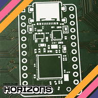
Routed the PCB and Designed
This was a doosey. As the second time routing a PCB I found this to be a hugely time consuming step. At the start I just began routing, but as I was luckily informed some things have certain requirments, e.g. USB D+ and D- need to be the same length, and that the MicroSD card routes should try to be via-less.
However, through hours of turmoil and restarts I believe that I have a much greater grasp on the process of routing a PCB which is what I am most happy with.
**Note: I spent way more time on this step then usual due to mistakes and slow work.
Courtesy to the guide by Kai, I went ahead and added some design to my PCB putting a small Gojo on the front and a large Gojo on the back.


jakeperrin2307
added to the journal ago
Organised everything to do with the PCB
Here I got to do the pleasure of organising everything. The initial stages was a bit daunting with all of the seemingly random capacitors and resistors, but after a bit it become very manageable.

jakeperrin2307
added to the journal ago
Assigned Footprints
Following the guide, I have assigned all the relevant footprints for the schematic. The hardest part was figuring out the footprints of the symbols not used in the guide, like the MicroSD card reader and Ferrite bead, but with some searches I manage to figure it our pretty easily.

jakeperrin2307
added to the journal ago
Finalised PCB Schematic
With the help of friends on Reddit, I have finish the schematic. This devboard includes USB-C power, a MicroSD card slot, UART, JTAG, a reset button, a boot button, and an I2C connector.
The most difficult part about this process was knowing if what I added was correct or not, and if it needed changes, what those changes were. This is where other people really helped, as they gave a bunch of guidance and explained things to me.

jakeperrin2307
added to the journal ago
Finished the 1st iteration of the schematic
Choosing a different micro-controller than in the guide proved to be quite time consuming, even following and reading through the datasheet. I had many questions that couldn't be answered just by reading a bit more through the guide, but this is where I found ChatGPT and the Slack chat very useful. This was the main challenge that I found, getting to where I am now is quite rewarding.
There may be some mistakes that I need to correct, but overall this is the first iteration of the schematic.

jakeperrin2307
added to the journal ago
Working on Power and USB-C
Working on the PCB, I imported the relevant symbols and got to work on the power for the devboard. I decided on USB-C similar to the guide, but rather than a NCP1117, I was going to use a buck switching regulator. I got most of teh way through before I realised that I was likely overcomplicating something simple. So I went back to the drawing board and decided on a MCP1700 120xxMB, which was alot simpler and easy.


jakeperrin2307
added to the journal ago
Research devboards.
Before starting the project I didn't know what a devboard is or what it is used for, so before making one I wanted to know this. I used a combination of ChatGPT and the internet to ask questions and build up knowledge of what it is and what they are used for.
I also planned for what modifications I will make to differ from the guide, and think about what the purpose of the devboard will be in my circumstance.
Overall, ChatGPT was very helpful as it could explain anything I wasn't understanding and also give me fast information.

jakeperrin2307
started ESP32 Devboard ago
12/9/2025 11 AM - Research devboards.
Before starting the project I didn't know what a devboard is or what it is used for, so before making one I wanted to know this. I used a combination of ChatGPT and the internet to ask questions and build up knowledge of what it is and what they are used for.
I also planned for what modifications I will make to differ from the guide, and think about what the purpose of the devboard will be in my circumstance.
Overall, ChatGPT was very helpful as it could explain anything I wasn't understanding and also give me fast information.
12/9/2025 1 PM - Working on Power and USB-C
Working on the PCB, I imported the relevant symbols and got to work on the power for the devboard. I decided on USB-C similar to the guide, but rather than a NCP1117, I was going to use a buck switching regulator. I got most of teh way through before I realised that I was likely overcomplicating something simple. So I went back to the drawing board and decided on a MCP1700 120xxMB, which was alot simpler and easy.
12/9/2025 6 PM - Finished the 1st iteration of the schematic
Choosing a different micro-controller than in the guide proved to be quite time consuming, even following and reading through the datasheet. I had many questions that couldn't be answered just by reading a bit more through the guide, but this is where I found ChatGPT and the Slack chat very useful. This was the main challenge that I found, getting to where I am now is quite rewarding.
There may be some mistakes that I need to correct, but overall this is the first iteration of the schematic.
12/10/2025 - Finalised PCB Schematic
With the help of friends on Reddit, I have finish the schematic. This devboard includes USB-C power, a MicroSD card slot, UART, JTAG, a reset button, a boot button, and an I2C connector.
The most difficult part about this process was knowing if what I added was correct or not, and if it needed changes, what those changes were. This is where other people really helped, as they gave a bunch of guidance and explained things to me.
12/11/2025 3 PM - Assigned Footprints
Following the guide, I have assigned all the relevant footprints for the schematic. The hardest part was figuring out the footprints of the symbols not used in the guide, like the MicroSD card reader and Ferrite bead, but with some searches I manage to figure it our pretty easily.
12/11/2025 9 PM - Organised everything to do with the PCB
Here I got to do the pleasure of organising everything. The initial stages was a bit daunting with all of the seemingly random capacitors and resistors, but after a bit it become very manageable.
12/12/2025 7 PM - Routed the PCB and Designed
This was a doosey. As the second time routing a PCB I found this to be a hugely time consuming step. At the start I just began routing, but as I was luckily informed some things have certain requirments, e.g. USB D+ and D- need to be the same length, and that the MicroSD card routes should try to be via-less.
However, through hours of turmoil and restarts I believe that I have a much greater grasp on the process of routing a PCB which is what I am most happy with.
**Note: I spent way more time on this step then usual due to mistakes and slow work.
Courtesy to the guide by Kai, I went ahead and added some design to my PCB putting a small Gojo on the front and a large Gojo on the back.
12/12/2025 8 PM - Created the production ZIP
**Before the last step, spent a fair chunk of time double checking the PCB to make sure everything was correct, e.g. DRC.
Last step so that the project is ready to be produced/assembled is to create the ZIP file with all of the relevant GERBER, DRILL, BOM and Footprint position files. I exported the drill and gerber files normally, but the BOM and Footprint position files needed to be modified.
For the Footprint position, the subheadings changed: Ref -> Designator, PosX -> Mid X, PosY -> Mid Y, Rot -> Rotation, and Side -> Layer.
For the BOM, the subheading changed: Designation -> Comment.
Finally, all of these files are compressed into a ZIP.
12/15/2025 - Created and finalised a Github page for the project
Spent some time finishing off the GitHub page and getting it into a proper usable state. Added the main project files, including the schematic, PCB layout, BOM, and placement files, so anyone looking at the repo can actually see how the board is designed. With everything uploaded and organised, the project feels complete.