5.8GHz Drone FPV Reciever
A 5GHz receiver PCB for use with any FPV drone. It runs off of a LiPo battery connected to the PCB that it also charges when connected by USB-C. It decodes the video signal and provides output to a 40pin FFC connector for a 40pin parallel 3x8 RGB display.
Created by
 CircuitGuy
Tier 1
9 views
0 followers
 CAN ⚡🚀
approved 5.8GHz Drone FPV Reciever ago
CAN ⚡🚀
approved 5.8GHz Drone FPV Reciever ago
Tier approved: 1
Grant approved: $263.00
Awesome project!
CircuitGuy
submitted 5.8GHz Drone FPV Reciever for ship review ago
CircuitGuy
added to the journal ago
Made some very nice renders using Fusion
Used Fusion 360 and it's render functionality to make some nicer renders and show the functionality of the case! (I also added an Ethix Mad Mushroom Antenna just to complete the model, however I'll probably not be ordering that as it's not the cheapest option out there and quite expensive)


CircuitGuy
added to the journal ago
Modelled a friction fit case
My recently acquired Elegoo Neptune 4 seems to have perfectly calibrated dimensional accuracy (unlike my older ender 3), to the point where a ring on a cylinder, with no clearance in-between the two, they will slide in perfectly with the right amount of friction to get a good hold. So I decided to leverage that and make my life easier by creating a friction fit case. This way I don't have to use and heated inserts and screws to keep it shut and I don't have to trial different clearance options as I already have the perfect amount of friction at zero clearance.
First I started of by making a basic covering around the PCB, display and battery, I also added the cylinders that will hold the PCB from moving horizontally out of place and then split the shape I just made in two. Then I just extruded only 2mm from the Top half of the case downwards so the Top covered the top and the the whole of the sides while the Bottom wasn't very visible, pictures explain it better. This also gave for much better visuals as the seam from there being two separate parts will no longer be halfway up the side but rather on the bottom which is much nicer and more hidden away.


Edit: Almost forgot the USB C and power switch opening xd

CircuitGuy
added to the journal ago
Added 3D PCB model into fusion and modelled display/battery
Exported the PCB's 3d model into fusion, then modelled the screen and the LiPo battery. Nothing exact just enough for me to design the case for the module. I plan on using the three holes I've added onto the board to align the board onto the case and then use M2 screws and heated inserts to hold the case closed.
CircuitGuy
added to the journal ago
Checked DRC
Spent some time checking DRC too to make sure everything is fine. It happens I had some vias that were too small and some of the them were too close to traces so I had to redo quite a few vias, apart from that a lot of silkscreen clipped by board edge and overlapping silkscreen but I can safely ignore that as I think you can see why that's happening from the picture xd.

CircuitGuy
added to the journal ago
Added some super cool silkscreen patterns
Spent a bunch of hours trying to figure out how to work Inkscape, vectorizing tools, getting scale right but all worth it to get these super cool patterns on my board. Took me so long because I also had to figure out how to mask an area from the pattern, then create all the masks for the components and export it like that so the pattern didn't cover silkscreen/components. I also did it for the back and front.


CircuitGuy
added to the journal ago
Cleaned up silkscreen and board look.
- Added exposed copper where the display legs grip, they're metal and I want the entire display to be connected to the ground plane, probably won't do much but it'll do more good than harm to have a bigger ground plane, because high ground plane means less interference absorption.
- Filleted the board, had to split it into each individual lines and then fillet those to not fillet the tabs for the display casing too
- Add some really cool exposed copper text and silkscreen around the board using this also really cool font that I found, so now all the silkscreen is cleaned up.


CircuitGuy
added to the journal ago
Finished off the rest of the board's traces
Routed the rest of power, I did my best to pay attention to current capacity of traces, even though I am on the safe side by a big margin for pretty much all the traces, but I'm still hoping the switching power converters will work (I've got trauma from the last time xd).
I also used KiCad's built in impedance calculator to work out a 75 Ohm trace for the video signal from the RTX module to the decoder chip and to work out the 50 Ohm trace for the antenna signal, and routed those and surrounded with ground accordingly to the type of impedance matching I'm using (coplanar with ground plane).
I also routed the rest of the I2C signals that go around the board, the LEDs, the buttons, the debug/extras headers on the edge of the board and all the other miscellaneous traces.
Now I need to sort out 3D models, DRC check, put some nice silkscreen on, then case, then renders, then done!


CircuitGuy
added to the journal ago
Routed everything necessary for the MCU.
Routed all the decoupling caps, the flash chips, and even the LED traces that go to the end of the board. I had to change the flash chip for a smaller package, not really that needed but I realised there were smaller packages available which are much nicer to route. (While doing all these specific sections I've also been routing the general power routes around the board)

CircuitGuy
added to the journal ago
Routed 5V switching power converter.
Paid very acute attention to the design guide and tried to follow it as much as possible. Pretty much on spot except, by having to use bigger vias, I ended up with a few less vias on the inductor SW nodes than the example layout shows, however the example layout also sacrificed the distance of the inductor from the IC for the closeness of the 0402 decoupling caps. So I figured this would be fine.

CircuitGuy
added to the journal ago
Vias too small, had to redo routing for decoder to FPC conn
The vias I was using were way too tiny and added £50 to the PCB cost. So I redid the connector traces with bigger vias to reduce the cost. However this time I have traces longer by 10mm on average. Still well under 100mm though so it's fine.

CircuitGuy
added to the journal ago
Routed clock lines for the display from the decoder.
Routed the clock lines from the display to the decoder, they run at about 33MHz max (pixel clock) so it's not that big a deal keeping them the same length, but they vary from 8mm to 24mm, which shouldn't be a problem nonetheless but I made sure the pixel clock line was 24mm+ to be safe, so it reads data only once all the other signals have arrived.

CircuitGuy
added to the journal ago
Put all of components in their layouts an positions.
Used the datasheet for the layouts for all the components to find their best positions on the board and routed them. The 24V switch converted didn't actually have a datasheet layout example I could use, but I think before I didn't have enough trace area between the switching components so I made sure of that now. I had to try a few positions, originally I was thinking having everything to one side but that was with an 18650 cell and it's holder, now that I have a LiPo pack, they tend to have dimensions more square than long so I had to try and shove everything up top. This should be fine hopefully as long as I pay close attention to RF traces and separate power/signal traces accordingly. I've also decided to use a stackup of:
L1 - Video trace + Signals
L2 - GND
L3 - More signals + Power
L4 - GND + Power
Of course I can deviate from that but that gives me a rough idea of what level to start routing everything.

CircuitGuy
added to the journal ago
Cleaned up the Schematic.
Cleaned up the schematic, spread out components, added the correct FPC connector (I need top contact, not bottom contact), made sure all the voltages and troubleshoot headers are correct and checked DRC. I can now move onto the PCB.

CircuitGuy
added to the journal ago
Added MCU, RP2040.
Decided to use a different MCU instead of the ATmega328P and I went with the RP2040, it's slightly easier to use and much more powerful, which is a nice have, it's not more expensive than the ATMega either. Added all the necessary connections to I2C lines, resistive display touch pins, LEDs, added flash and crystal for the RP2040 and control buttons/decoupling caps.

CircuitGuy
added to the journal ago
Added and wired up the TW8819.
This part took a while...
The datasheet isn't the best for this specific part, it mentioned supply from 3.3V and 1.8V but it didn't make it clear whether it was either 1.8V OR 3.3V or 1.8V AND 3.3V required, and if it's the first, I wouldn't want to back feed any internal circuitry for voltage inside the TW8819. But after looking around a bit I managed to figure out it needs two separate supplies as each one has different power consumptions.
Then once that confusion was over, I connected up a suitable crystal to run the chip and the power lines / data lines to the chip plus decoupling caps and all the nets for the display/video

CircuitGuy
added to the journal ago
Setup LEDs, nets for TFT pins and backlight driver.
Added the LED 24V boost and current limiting circuit for the TFT Display. I think the circuitry is fine, and the original problem on my old circuit was fully just stupid layout, because adding more copper area (a copper wire) to the trace between the inductor and diode seems to have fixed the issue completely, and only moving the wire around seems to affect it so. I just need to follow the datasheet layout biblically (and probably for the 5V buck/boost too) to make sure I don't have those headaches this time.
Also wired up some LEDs and required current limiting resistors. I was careful to use the basic component LEDs available by JLCPCB to try and reduce some cost. And the big FFC connector for the display too after finding out the right one. It turns out I need one with the contacts on top, but I had one with contacts on bottom and GOD ARE THERE MANY FPCS OUT THERE, I had to sift through about a thousand different variations just to find something that MIGHT fit.

CircuitGuy
added to the journal ago
Added the RX5808 module and wired it up.
As the title says, I added the RX5808 board and wired it up. Much similar to the TX5813 board with the DIP switches for band selection, caps and SMA connector, however this time there was the RSSI connector for signal strength indication which I will connect to an ADC input on the ATmega328 chip. The RX5808 will have to be bought separately and soldered by myself, like the TX5813 as JLCPCB doesn't seem to have anything in stock.

CircuitGuy
added to the journal ago
Added 1.8/3.3V LDOs and circuitry for 5V buck/boost.
Added the LDOs (LD1117, not the AMS ones as these seem to be a bit controversial...) and more or less copied over the circuitry for the 5V buck/boost from the FC design. I had bad experiences with the buck/boost converter for 24V on another TFT display board, however that was due to very poor and ignorant layout, which I'm paying attention to now but I hope there won't be any other problems with these sensitive circuits as that would kind of ruin the whole board.

CircuitGuy
added to the journal ago
Setup USB-C and BQ charger chip
USB C connector wired up with CC resistors and data nets added. Also added the BQ and it's supporting circuitry and decoupling caps with the connector for the battery 1s pack. The BQ seems to have I2C control as well so I'll connected that up to the MCU as well. I also added a switch to turn the whole system on/off, however this will not stop the battery from charging off of USB C. Pretty straightforward stuff so far.

CircuitGuy
added to the journal ago
Plan out and research for the Recept PCB
This project is designed to go hand in hand with another blueprint project of mine, the flight controller, which has the 5GHz FPV emitting circuitry built in. This is designed to be the receiving side, a fully contained system, only about 10cm thick, and the size of the display that's gonna be used, full with LiPo battery and USB charging. (I worked a little bit on this in the FC project journaling but I decided to create a new project out of it to keep things simple so I deleted the journals there and moved the hours here, hence the seemingly 13 hours in an afternoon on the first day).
I was originally deciding to use a 18650 battery. However, that has a very tall profile, is quite heavy and doesn't use the space as efficiently. A much better option would be to use a LiPo pack, these can be much thinner, to make for a nicer case. Connection can just be a simple solder connection as the battery isn't designed to be removable and they also hold more charge. This means I can compact my circuitry as much as I can (the board size is constrained to the size of the 4.3" TFT) and then order an appropriate 1s thin LiPo pack to use up the rest of the PCB space. This is just a much cleaner option than an 18650 cell.
The whole circuitry will be mounted on a PCB that latches directly onto the back of a TFT display (4.3") that has a special case with clips to hold onto the PCB. I will also design a case later on once I'm finalized with the antenna placement (that and the USB C may have to be detached from underneath the display as they're through hole components.
Doing some research, I will be using the BQ21088YBGR charger IC. Perfect for my use case as it provides power path support so easy integration and charges 1s with only 1A (I don't need much more). However, only thing to look out for is that it's a very small BGA package, this might make it hard to troubleshoot but assembly should be fine (there will be other extended/standard components anyways). That's battery, charging and VSYS sorted.
In terms of 5GHz receiver I will be using the RX5808, besides being the cheapest easy to use module in existence (I don't like RF), it also seems to be the cousin of the TX5813 (which is on my FC, on the other project). Also with just a generic SMA connecter for the antenna.
I'll also be using a TW8819, this seems to be the cheapest and easily accessible chip from the TW88xx class. I had to use this because I need an easy to use converter from composite video in from the RX module and parallel 3x8 RGB out for the TFT display, and this chip is designed to do just that!
However the TW8819 needs an MCU to configure it's I2C registers. I was originally going to go with an ESP32 however, that's quite overkill for just configuring registers and monitoring the odd voltage/RSSI. So I will probably use a much lighter Atmega328P (or whatever chip the Arduino Uno uses) running off of 3.3V.
In terms of power... The TW8819 will need 3.3V (and the Arduino) and 1.8V but they won't consume much, so I can just use simple LDOs. But for the 5V rail, since the battery only provides minimum 3V (planned dropout) I will need a 5V buck/boost to raise to the needed voltage when needed and because an LDO is not enough for the ~200mA consumption of the RX module. The 1.8V LDO can run safely straight from system however the 3.3V LDO will have to run from the 5V converter as it wouldn't have enough voltage from the battery. In terms of 5V buck/boost I will use the TPS63070 simply because that's already what I used in the flight controller so I don't have to redo another design. I also have an MT3608 raising voltage to 24V for the LED backlight of the display and a CAT4104 limiting current for it.
LEDs I plan to use will be power indicators and 8 GPIO LEDs to give an indication of power level corresponding to the voltage divider reading the battery.

CircuitGuy
started 5.8GHz Drone FPV Reciever ago
3/10/2026 6:34 PM - Plan out and research for the Recept PCB
This project is designed to go hand in hand with another blueprint project of mine, the flight controller, which has the 5GHz FPV emitting circuitry built in. This is designed to be the receiving side, a fully contained system, only about 10cm thick, and the size of the display that's gonna be used, full with LiPo battery and USB charging. (I worked a little bit on this in the FC project journaling but I decided to create a new project out of it to keep things simple so I deleted the journals there and moved the hours here, hence the seemingly 13 hours in an afternoon on the first day).
I was originally deciding to use a 18650 battery. However, that has a very tall profile, is quite heavy and doesn't use the space as efficiently. A much better option would be to use a LiPo pack, these can be much thinner, to make for a nicer case. Connection can just be a simple solder connection as the battery isn't designed to be removable and they also hold more charge. This means I can compact my circuitry as much as I can (the board size is constrained to the size of the 4.3" TFT) and then order an appropriate 1s thin LiPo pack to use up the rest of the PCB space. This is just a much cleaner option than an 18650 cell.
The whole circuitry will be mounted on a PCB that latches directly onto the back of a TFT display (4.3") that has a special case with clips to hold onto the PCB. I will also design a case later on once I'm finalized with the antenna placement (that and the USB C may have to be detached from underneath the display as they're through hole components.
Doing some research, I will be using the BQ21088YBGR charger IC. Perfect for my use case as it provides power path support so easy integration and charges 1s with only 1A (I don't need much more). However, only thing to look out for is that it's a very small BGA package, this might make it hard to troubleshoot but assembly should be fine (there will be other extended/standard components anyways). That's battery, charging and VSYS sorted.
In terms of 5GHz receiver I will be using the RX5808, besides being the cheapest easy to use module in existence (I don't like RF), it also seems to be the cousin of the TX5813 (which is on my FC, on the other project). Also with just a generic SMA connecter for the antenna.
I'll also be using a TW8819, this seems to be the cheapest and easily accessible chip from the TW88xx class. I had to use this because I need an easy to use converter from composite video in from the RX module and parallel 3x8 RGB out for the TFT display, and this chip is designed to do just that!
However the TW8819 needs an MCU to configure it's I2C registers. I was originally going to go with an ESP32 however, that's quite overkill for just configuring registers and monitoring the odd voltage/RSSI. So I will probably use a much lighter Atmega328P (or whatever chip the Arduino Uno uses) running off of 3.3V.
In terms of power... The TW8819 will need 3.3V (and the Arduino) and 1.8V but they won't consume much, so I can just use simple LDOs. But for the 5V rail, since the battery only provides minimum 3V (planned dropout) I will need a 5V buck/boost to raise to the needed voltage when needed and because an LDO is not enough for the ~200mA consumption of the RX module. The 1.8V LDO can run safely straight from system however the 3.3V LDO will have to run from the 5V converter as it wouldn't have enough voltage from the battery. In terms of 5V buck/boost I will use the TPS63070 simply because that's already what I used in the flight controller so I don't have to redo another design. I also have an MT3608 raising voltage to 24V for the LED backlight of the display and a CAT4104 limiting current for it.
LEDs I plan to use will be power indicators and 8 GPIO LEDs to give an indication of power level corresponding to the voltage divider reading the battery.
3/10/2026 6:37 PM - Setup USB-C and BQ charger chip
USB C connector wired up with CC resistors and data nets added. Also added the BQ and it's supporting circuitry and decoupling caps with the connector for the battery 1s pack. The BQ seems to have I2C control as well so I'll connected that up to the MCU as well. I also added a switch to turn the whole system on/off, however this will not stop the battery from charging off of USB C. Pretty straightforward stuff so far.
3/10/2026 6:39 PM - Added 1.8/3.3V LDOs and circuitry for 5V buck/boost.
Added the LDOs (LD1117, not the AMS ones as these seem to be a bit controversial...) and more or less copied over the circuitry for the 5V buck/boost from the FC design. I had bad experiences with the buck/boost converter for 24V on another TFT display board, however that was due to very poor and ignorant layout, which I'm paying attention to now but I hope there won't be any other problems with these sensitive circuits as that would kind of ruin the whole board.
3/10/2026 6:41 PM - Added the RX5808 module and wired it up.
As the title says, I added the RX5808 board and wired it up. Much similar to the TX5813 board with the DIP switches for band selection, caps and SMA connector, however this time there was the RSSI connector for signal strength indication which I will connect to an ADC input on the ATmega328 chip. The RX5808 will have to be bought separately and soldered by myself, like the TX5813 as JLCPCB doesn't seem to have anything in stock.
3/10/2026 6:47 PM - Setup LEDs, nets for TFT pins and backlight driver.
Added the LED 24V boost and current limiting circuit for the TFT Display. I think the circuitry is fine, and the original problem on my old circuit was fully just stupid layout, because adding more copper area (a copper wire) to the trace between the inductor and diode seems to have fixed the issue completely, and only moving the wire around seems to affect it so. I just need to follow the datasheet layout biblically (and probably for the 5V buck/boost too) to make sure I don't have those headaches this time.
Also wired up some LEDs and required current limiting resistors. I was careful to use the basic component LEDs available by JLCPCB to try and reduce some cost. And the big FFC connector for the display too after finding out the right one. It turns out I need one with the contacts on top, but I had one with contacts on bottom and GOD ARE THERE MANY FPCS OUT THERE, I had to sift through about a thousand different variations just to find something that MIGHT fit.
3/10/2026 6:50 PM - Added and wired up the TW8819.
This part took a while...
The datasheet isn't the best for this specific part, it mentioned supply from 3.3V and 1.8V but it didn't make it clear whether it was either 1.8V OR 3.3V or 1.8V AND 3.3V required, and if it's the first, I wouldn't want to back feed any internal circuitry for voltage inside the TW8819. But after looking around a bit I managed to figure out it needs two separate supplies as each one has different power consumptions.
Then once that confusion was over, I connected up a suitable crystal to run the chip and the power lines / data lines to the chip plus decoupling caps and all the nets for the display/video
3/10/2026 9 PM - Added MCU, RP2040.
Decided to use a different MCU instead of the ATmega328P and I went with the RP2040, it's slightly easier to use and much more powerful, which is a nice have, it's not more expensive than the ATMega either. Added all the necessary connections to I2C lines, resistive display touch pins, LEDs, added flash and crystal for the RP2040 and control buttons/decoupling caps.
3/10/2026 10 PM - Cleaned up the Schematic.
Cleaned up the schematic, spread out components, added the correct FPC connector (I need top contact, not bottom contact), made sure all the voltages and troubleshoot headers are correct and checked DRC. I can now move onto the PCB.
3/14/2026 10:16 AM - Put all of components in their layouts an positions.
Used the datasheet for the layouts for all the components to find their best positions on the board and routed them. The 24V switch converted didn't actually have a datasheet layout example I could use, but I think before I didn't have enough trace area between the switching components so I made sure of that now. I had to try a few positions, originally I was thinking having everything to one side but that was with an 18650 cell and it's holder, now that I have a LiPo pack, they tend to have dimensions more square than long so I had to try and shove everything up top. This should be fine hopefully as long as I pay close attention to RF traces and separate power/signal traces accordingly. I've also decided to use a stackup of:
L1 - Video trace + Signals
L2 - GND
L3 - More signals + Power
L4 - GND + Power
Of course I can deviate from that but that gives me a rough idea of what level to start routing everything.
3/14/2026 10:44 AM - Routed clock lines for the display from the decoder.
Routed the clock lines from the display to the decoder, they run at about 33MHz max (pixel clock) so it's not that big a deal keeping them the same length, but they vary from 8mm to 24mm, which shouldn't be a problem nonetheless but I made sure the pixel clock line was 24mm+ to be safe, so it reads data only once all the other signals have arrived.
3/14/2026 10 PM - Vias too small, had to redo routing for decoder to FPC conn
The vias I was using were way too tiny and added £50 to the PCB cost. So I redid the connector traces with bigger vias to reduce the cost. However this time I have traces longer by 10mm on average. Still well under 100mm though so it's fine.
3/15/2026 6 PM - Routed 5V switching power converter.
Paid very acute attention to the design guide and tried to follow it as much as possible. Pretty much on spot except, by having to use bigger vias, I ended up with a few less vias on the inductor SW nodes than the example layout shows, however the example layout also sacrificed the distance of the inductor from the IC for the closeness of the 0402 decoupling caps. So I figured this would be fine.
3/15/2026 8 PM - Routed everything necessary for the MCU.
Routed all the decoupling caps, the flash chips, and even the LED traces that go to the end of the board. I had to change the flash chip for a smaller package, not really that needed but I realised there were smaller packages available which are much nicer to route. (While doing all these specific sections I've also been routing the general power routes around the board)
3/16/2026 - Finished off the rest of the board's traces
Routed the rest of power, I did my best to pay attention to current capacity of traces, even though I am on the safe side by a big margin for pretty much all the traces, but I'm still hoping the switching power converters will work (I've got trauma from the last time xd).
I also used KiCad's built in impedance calculator to work out a 75 Ohm trace for the video signal from the RTX module to the decoder chip and to work out the 50 Ohm trace for the antenna signal, and routed those and surrounded with ground accordingly to the type of impedance matching I'm using (coplanar with ground plane).
I also routed the rest of the I2C signals that go around the board, the LEDs, the buttons, the debug/extras headers on the edge of the board and all the other miscellaneous traces.
Now I need to sort out 3D models, DRC check, put some nice silkscreen on, then case, then renders, then done!
3/17/2026 - Cleaned up silkscreen and board look.
- Added exposed copper where the display legs grip, they're metal and I want the entire display to be connected to the ground plane, probably won't do much but it'll do more good than harm to have a bigger ground plane, because high ground plane means less interference absorption.
- Filleted the board, had to split it into each individual lines and then fillet those to not fillet the tabs for the display casing too
- Add some really cool exposed copper text and silkscreen around the board using this also really cool font that I found, so now all the silkscreen is cleaned up.
3/18/2026 8 PM - Added some super cool silkscreen patterns
Spent a bunch of hours trying to figure out how to work Inkscape, vectorizing tools, getting scale right but all worth it to get these super cool patterns on my board. Took me so long because I also had to figure out how to mask an area from the pattern, then create all the masks for the components and export it like that so the pattern didn't cover silkscreen/components. I also did it for the back and front.
3/18/2026 9 PM - Checked DRC
Spent some time checking DRC too to make sure everything is fine. It happens I had some vias that were too small and some of the them were too close to traces so I had to redo quite a few vias, apart from that a lot of silkscreen clipped by board edge and overlapping silkscreen but I can safely ignore that as I think you can see why that's happening from the picture xd.
3/19/2026 5 PM - Added 3D PCB model into fusion and modelled display/battery
Exported the PCB's 3d model into fusion, then modelled the screen and the LiPo battery. Nothing exact just enough for me to design the case for the module. I plan on using the three holes I've added onto the board to align the board onto the case and then use M2 screws and heated inserts to hold the case closed.


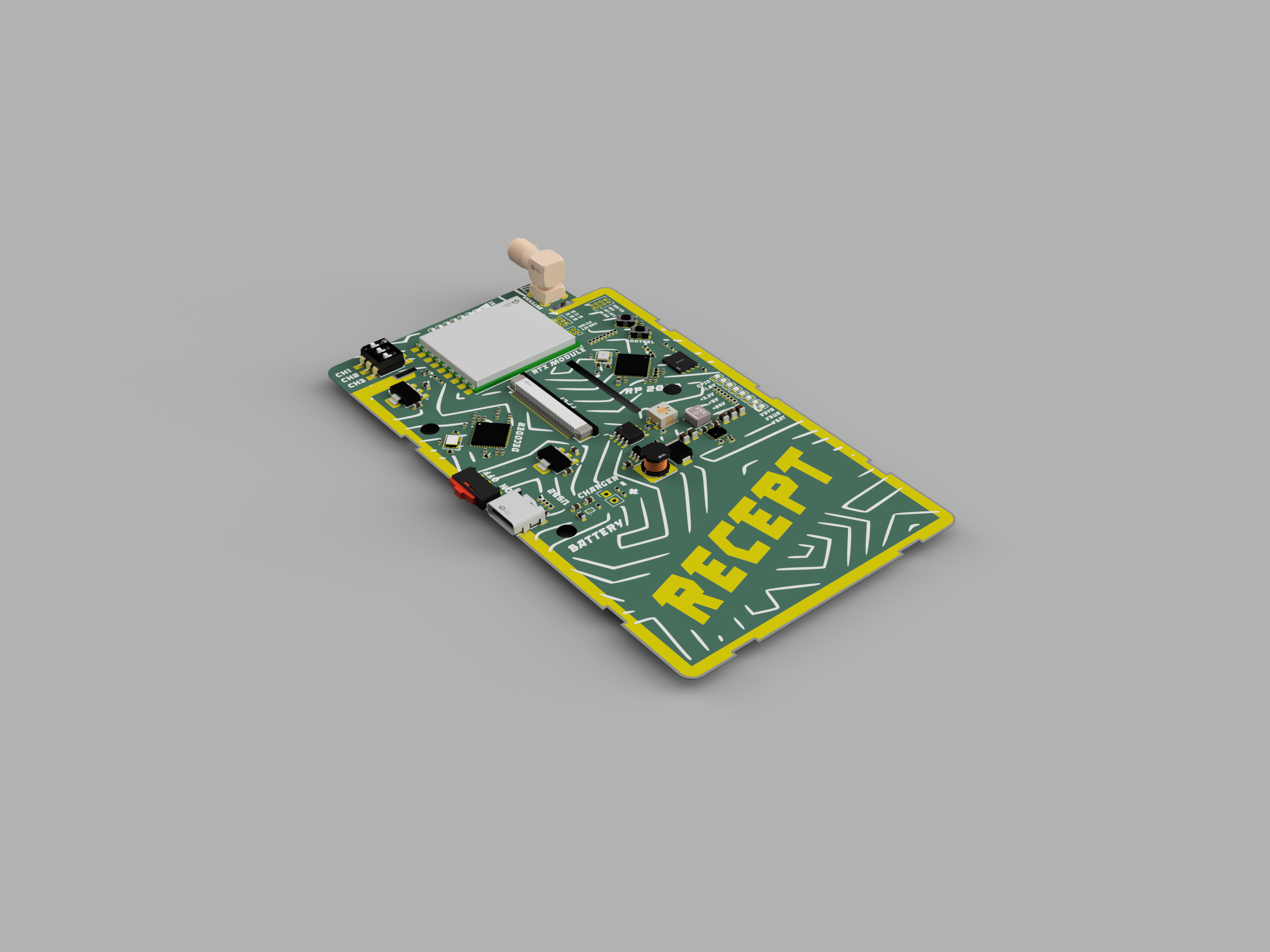
First high definition render of the PCB
3/19/2026 9 PM - Modelled a friction fit case
My recently acquired Elegoo Neptune 4 seems to have perfectly calibrated dimensional accuracy (unlike my older ender 3), to the point where a ring on a cylinder, with no clearance in-between the two, they will slide in perfectly with the right amount of friction to get a good hold. So I decided to leverage that and make my life easier by creating a friction fit case. This way I don't have to use and heated inserts and screws to keep it shut and I don't have to trial different clearance options as I already have the perfect amount of friction at zero clearance.
First I started of by making a basic covering around the PCB, display and battery, I also added the cylinders that will hold the PCB from moving horizontally out of place and then split the shape I just made in two. Then I just extruded only 2mm from the Top half of the case downwards so the Top covered the top and the the whole of the sides while the Bottom wasn't very visible, pictures explain it better. This also gave for much better visuals as the seam from there being two separate parts will no longer be halfway up the side but rather on the bottom which is much nicer and more hidden away.
Edit: Almost forgot the USB C and power switch opening xd
3/23/2026 - Made some very nice renders using Fusion
Used Fusion 360 and it's render functionality to make some nicer renders and show the functionality of the case! (I also added an Ethix Mad Mushroom Antenna just to complete the model, however I'll probably not be ordering that as it's not the cheapest option out there and quite expensive)