My NFC Reader
An NFC reader project for reading and identifying NFC tags and cards
Created by
 Prince
Tier 3
12 views
0 followers
 Kai the Jolly Guy 🚀
rejected My NFC Reader ago
Kai the Jolly Guy 🚀
rejected My NFC Reader ago
User is banned for frauding projects!
Prince
added to the journal ago
Photo update

Because of prev. journal the photo changed so this journal is regarding the photo update i have asked for 75$ reducing from 78$ bcz i will use E-Post for delivery which reduced 3$ spprox.
Prince
submitted My NFC Reader for ship review ago
Prince
added to the journal ago
Updated
I have updated the repo with the code due to a oversight I forgot to add it .. the reason for not using E-Post is because I'm unaware of its functionality in India and the difference is only 2$ but as per @Iamalive it is eligible so I would request for 2$ less this time thx.

 Iamalive 🚀
requested changes for My NFC Reader ago
Iamalive 🚀
requested changes for My NFC Reader ago
Great work on the project so far - didn't think that an ESP 32 could do nfc as well lol. Just two simple things left to fix! First is to make some sort of basic code for the board!(its fine if it ends up not working, as long as you tried your best to make something and learn the language). Next is actually just a question - is there a reason why you can't use E-Post? I downloaded your board and its only about 9cmx4.5cm, which should let it be eligible. Just explain in the note to reviewer when you resubmit!
Prince
submitted My NFC Reader for ship review ago
Prince
added to the journal ago
Price update


the total cost 80$ due to an oversight from my end i didnt update the screenshots of the cart.. all the parts are from jlcpcb as i have understood that thats the cheapest option out there in india
 PenguinMo
requested changes for My NFC Reader ago
PenguinMo
requested changes for My NFC Reader ago
This is looking but can you upload the pictures of the cart total on the website and you PCB cart total also as your project stands right now it is a tier 4 is you want to increase the tier please consider adding a case to be 3d printed also is there anyway to reduce the price, you might need to think out of the box . This project looks really cool and has some nice silkscreens, I can't wait to see you finish this build
Prince
submitted My NFC Reader for ship review ago
Prince
added to the journal ago
Full journal as i didnt post journals split after starting
Day 1 – Understanding NFC (4 Hours)
The project began with a very important question What exactly is NFC and how does it work without touching anything? The first few hours were spent understanding the basic concept of Near Field Communication and why it is used in metro cards, ID cards, and access systems Initially NFC sounded simple—just tap and go—but as I started reading I realized there is a lot happening behind that single tap.
I explored how NFC works at very short distances and how it uses electromagnetic fields instead of traditional wired connections Reading about ISO/IEC 14443 standards made me feel like I had entered a secret club of engineers who love numbers and specifications I also learned the difference between active and passive NFC devices which finally explained why NFC cards do not need batteries.
To make things more interesting I watched videos and read tutorials that explained NFC using real-life examples Suddenly, my daily metro travel made more sense I took notes, drew rough diagrams, and tried to simplify complex terms into something my future self would understand during exams.
By the end of Day 1 NFC no longer felt like magic. It felt like controlled well-documented engineering magic This foundation was necessary before touching any schematic or PCB because guessing in hardware design is usually a bad idea.
Day 2 – Component Selection & Datasheets (4 Hours)
Day 2 was dedicated to choosing components which sounds easy until you open a datasheet and see 50 pages of tiny text The goal was to select an NFC reader module or IC a suitable microcontroller and all supporting components such as resistors, capacitors, and connectors.
I spent a good amount of time understanding pin configurations voltage levels and communication interfaces like SPI or I2C Datasheets were read slowly sometimes twice because missing a small detail in hardware design can lead to very big regrets later.
At this stage I also thought about power requirements and how the circuit would be powered Choosing the wrong voltage regulator is an easy way to turn a project into a heater So extra care was taken to verify operating ranges and recommended configurations.
By the end of the day I had a finalized list of components and a much higher respect for engineers who write datasheets Everything was now ready to move from theory to actual design work.
Day 3 – Schematic Design (6 Hours)
This was the day when things became real Opening KiCad and starting a new schematic felt exciting and slightly scary The task was to convert all the knowledge from previous days into an actual circuit that makes sense electrically.
I carefully placed components connected power lines and ensured that communication pins were correctly routed Every connection was double-checked because unlike software hardware does not forgive careless mistakes.
Running ERC (Electrical Rule Check) was both helpful and humbling KiCad politely pointed out errors that I had confidently created Fixing these errors taught me a lot about proper grounding, power flags, and signal clarity.
By the end of the day the schematic was complete clean and understandable. Seeing a fully connected schematic felt like a major milestone in the project.
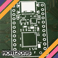
Day 4 – PCB Layout (7 Hours)
PCB layout day felt like solving a puzzle where every piece must fit perfectly. Component placement was done carefully to minimize routing complexity and ensure good signal flow especially around the NFC antenna area.
Routing tracks required patienc Power lines were kept thick signal lines neat and ground planes were added to reduce noise I learned that moving one component slightly can save hours of routing frustration.
Zooming in and out became a full-time activity Antenna placement received special attention because NFC performance depends heavily on proper layout.
By the end of the day the PCB looked clean organized and professional. It finally resembled something that could exist in the real world.
Day 5 – Review & Error Fixing (4 Hours)
Day 5 was all about not trusting yesterdays work blindly The PCB was reviewed carefully footprints were verified and DRC checks were run multiple times.
Small errors were found and fixed which proved why review is essential Correcting these issues before fabrication saves money, time, and emotional damage.
After a clean DRC report the design felt ready and reliable. This step added confidence to the entire project.
Day 6 – Documentation & Final Touches (4 Hours)
The final day focused on documentation and presentation Screenshots of the schematic and PCB were taken block diagrams were prepared and the project was explained in simple words.
Writing the journal helped reflect on how much was learned during the process What started as curiosity ended as a complete hardware design experience.
The project improved understanding of NFC technology PCB design and practical engineering workflow. It was challenging, educational, and genuinely satisfying.
Total Time Spent: 29 Hours
.png)

.png)
.png)


Prince
started My NFC Reader ago
12/31/2025 - Full journal as i didnt post journals split after starting
Day 1 – Understanding NFC (4 Hours)
The project began with a very important question What exactly is NFC and how does it work without touching anything? The first few hours were spent understanding the basic concept of Near Field Communication and why it is used in metro cards, ID cards, and access systems Initially NFC sounded simple—just tap and go—but as I started reading I realized there is a lot happening behind that single tap.
I explored how NFC works at very short distances and how it uses electromagnetic fields instead of traditional wired connections Reading about ISO/IEC 14443 standards made me feel like I had entered a secret club of engineers who love numbers and specifications I also learned the difference between active and passive NFC devices which finally explained why NFC cards do not need batteries.
To make things more interesting I watched videos and read tutorials that explained NFC using real-life examples Suddenly, my daily metro travel made more sense I took notes, drew rough diagrams, and tried to simplify complex terms into something my future self would understand during exams.
By the end of Day 1 NFC no longer felt like magic. It felt like controlled well-documented engineering magic This foundation was necessary before touching any schematic or PCB because guessing in hardware design is usually a bad idea.
Day 2 – Component Selection & Datasheets (4 Hours)
Day 2 was dedicated to choosing components which sounds easy until you open a datasheet and see 50 pages of tiny text The goal was to select an NFC reader module or IC a suitable microcontroller and all supporting components such as resistors, capacitors, and connectors.
I spent a good amount of time understanding pin configurations voltage levels and communication interfaces like SPI or I2C Datasheets were read slowly sometimes twice because missing a small detail in hardware design can lead to very big regrets later.
At this stage I also thought about power requirements and how the circuit would be powered Choosing the wrong voltage regulator is an easy way to turn a project into a heater So extra care was taken to verify operating ranges and recommended configurations.
By the end of the day I had a finalized list of components and a much higher respect for engineers who write datasheets Everything was now ready to move from theory to actual design work.
Day 3 – Schematic Design (6 Hours)
This was the day when things became real Opening KiCad and starting a new schematic felt exciting and slightly scary The task was to convert all the knowledge from previous days into an actual circuit that makes sense electrically.
I carefully placed components connected power lines and ensured that communication pins were correctly routed Every connection was double-checked because unlike software hardware does not forgive careless mistakes.
Running ERC (Electrical Rule Check) was both helpful and humbling KiCad politely pointed out errors that I had confidently created Fixing these errors taught me a lot about proper grounding, power flags, and signal clarity.
By the end of the day the schematic was complete clean and understandable. Seeing a fully connected schematic felt like a major milestone in the project.
Day 4 – PCB Layout (7 Hours)
PCB layout day felt like solving a puzzle where every piece must fit perfectly. Component placement was done carefully to minimize routing complexity and ensure good signal flow especially around the NFC antenna area.
Routing tracks required patienc Power lines were kept thick signal lines neat and ground planes were added to reduce noise I learned that moving one component slightly can save hours of routing frustration.
Zooming in and out became a full-time activity Antenna placement received special attention because NFC performance depends heavily on proper layout.
By the end of the day the PCB looked clean organized and professional. It finally resembled something that could exist in the real world.
Day 5 – Review & Error Fixing (4 Hours)
Day 5 was all about not trusting yesterdays work blindly The PCB was reviewed carefully footprints were verified and DRC checks were run multiple times.
Small errors were found and fixed which proved why review is essential Correcting these issues before fabrication saves money, time, and emotional damage.
After a clean DRC report the design felt ready and reliable. This step added confidence to the entire project.
Day 6 – Documentation & Final Touches (4 Hours)
The final day focused on documentation and presentation Screenshots of the schematic and PCB were taken block diagrams were prepared and the project was explained in simple words.
Writing the journal helped reflect on how much was learned during the process What started as curiosity ended as a complete hardware design experience.
The project improved understanding of NFC technology PCB design and practical engineering workflow. It was challenging, educational, and genuinely satisfying.
Total Time Spent: 29 Hours
1/5/2026 - Price update
the total cost 80$ due to an oversight from my end i didnt update the screenshots of the cart.. all the parts are from jlcpcb as i have understood that thats the cheapest option out there in india
1/17/2026 4 PM - Updated
I have updated the repo with the code due to a oversight I forgot to add it .. the reason for not using E-Post is because I'm unaware of its functionality in India and the difference is only 2$ but as per @Iamalive it is eligible so I would request for 2$ less this time thx.
1/17/2026 8 PM - Photo update
Because of prev. journal the photo changed so this journal is regarding the photo update i have asked for 75$ reducing from 78$ bcz i will use E-Post for delivery which reduced 3$ spprox.