 Tanuki ⚡🚀
approved MY NFC Card ago
Tanuki ⚡🚀
approved MY NFC Card ago
Tier approved: 5
Grant approved: $20.00
Great project! Enjoy the card :)
 Prince
submitted MY NFC Card for ship review ago
Prince
submitted MY NFC Card for ship review ago
Prince
added to the journal ago
update
I have changed the pcb partner which made the pcb cost $16.63 and the other components cost 0.07$(exclusive of shipping which is $0.56) when sourced from local partner. and also the bom.csv has been updated


 Iamalive 🚀
requested changes for MY NFC Card ago
Iamalive 🚀
requested changes for MY NFC Card ago
Hey, cool card but I'm going to have you to two things. First, can you fix your bom(https://github.com/PrinceYadav78/My-NFC-Card/blob/main/bom.csv) so that it includes price and the overall combined price? Also, can you maybe try to look into local/other pcb options? I know that jlcpcb is expensive becuase of imports, maybe other places like pcbcart? Thanks!
Prince
added to the journal ago
Price update
as per @penguinmo i have uploaded the gerber file to the repo... i agree with him for the shippping cost it seems high but wt to do india customs and jlcpcb shipping cost are at next level.. unfortunaly we cant do anything abt it.

Prince
submitted MY NFC Card for ship review ago
 PenguinMo
requested changes for MY NFC Card ago
PenguinMo
requested changes for MY NFC Card ago
This is really cool but can you upload your gerber files and took a picture of your shipping so we know it's the cheapest, I can't wait to see you build this
Prince
added to the journal ago
photo update
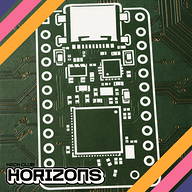
Upadting the photo as the banner photo isn't correct... didnt attach the photos in correct sequence in the last journal... i feel the nfc card looks cool

Prince
submitted MY NFC Card for ship review ago
Prince
added to the journal ago
My NFC Card Project Build Journal
Day One Four Hours
Day one was when i seriously started working on my NFC card project even though most planning was already done i still treated this day as fresh start i opened the repo and looked at everything again files images pcb and notes i wanted to be sure i still understood what i had built and why each part was there this took time but it was needed
I spent a long time reading again about NFC basics like how the card gets power from reader and how antenna plays biggest role i realized i earlier misunderstood few things about coupling and range so this review helped clear that confusion i did not rush because rushing in hardware usually ends badly
Then i looked at the NFC chip datasheet again some parts were still confusing but i tried to focus on important sections like memory structure and communication flow i also checked which phones can read it and what standards are supported this helped me feel sure that the card will work in real life
After that i went through the BOM and checked every component value footprint and package size i noticed some parts were very small and would need careful soldering i did not change anything but this step helped avoid mistakes later i also checked availability to be sure parts can be sourced
I then opened the schematic and slowly traced connections from chip to antenna and passive components i tried to understand why matching network was used and how small changes can affect performance this part was not easy but i stayed with it
The PCB layout took most of my attention i followed antenna path many times and imagined current flowing i checked spacing ground clearance and placement i did not change design but made sure i fully understood it
Before ending day one i checked card size and thickness to confirm it matches standard NFC cards this seems simple but is important for usability by the end of four hours my head felt heavy but i knew day one was successful because understanding was solid
Day Two Four Hours
Day two was more about finishing things and making sure project actually works i started by reviewing everything one last time schematic pcb and bom just to be safe because hardware gives no undo button
I generated gerber files and carefully checked them because exporting wrong settings can break everything i compared them visually with pcb layout to be sure antenna traces stayed correct
Then i thought about manufacturing details like board thickness copper layer and finish i wanted the card to be strong enough and still perform well so i made sure these choices matched NFC requirements
Assembly was done slowly because components were small and sensitive i paid attention to orientation and solder joints i tried to keep things clean and avoid overheating the NFC chip
Testing was the most important and satisfying part i used my phone to scan the card many times from different angles and distances it was detected consistently which showed antenna design was correct
I also tested reading and writing data multiple times to confirm memory works properly everything behaved stable and predictable which felt rewarding after all the careful work
At the end i updated the repository with final images and notes so that the project looks complete and understandable this project taught me that even simple looking hardware needs lot of patience and attention and completing it gave me confidence in working with NFC and RF based designs


Prince
started MY NFC Card ago
12/31/2025 - My NFC Card Project Build Journal
Day One Four Hours
Day one was when i seriously started working on my NFC card project even though most planning was already done i still treated this day as fresh start i opened the repo and looked at everything again files images pcb and notes i wanted to be sure i still understood what i had built and why each part was there this took time but it was needed
I spent a long time reading again about NFC basics like how the card gets power from reader and how antenna plays biggest role i realized i earlier misunderstood few things about coupling and range so this review helped clear that confusion i did not rush because rushing in hardware usually ends badly
Then i looked at the NFC chip datasheet again some parts were still confusing but i tried to focus on important sections like memory structure and communication flow i also checked which phones can read it and what standards are supported this helped me feel sure that the card will work in real life
After that i went through the BOM and checked every component value footprint and package size i noticed some parts were very small and would need careful soldering i did not change anything but this step helped avoid mistakes later i also checked availability to be sure parts can be sourced
I then opened the schematic and slowly traced connections from chip to antenna and passive components i tried to understand why matching network was used and how small changes can affect performance this part was not easy but i stayed with it
The PCB layout took most of my attention i followed antenna path many times and imagined current flowing i checked spacing ground clearance and placement i did not change design but made sure i fully understood it
Before ending day one i checked card size and thickness to confirm it matches standard NFC cards this seems simple but is important for usability by the end of four hours my head felt heavy but i knew day one was successful because understanding was solid
Day Two Four Hours
Day two was more about finishing things and making sure project actually works i started by reviewing everything one last time schematic pcb and bom just to be safe because hardware gives no undo button
I generated gerber files and carefully checked them because exporting wrong settings can break everything i compared them visually with pcb layout to be sure antenna traces stayed correct
Then i thought about manufacturing details like board thickness copper layer and finish i wanted the card to be strong enough and still perform well so i made sure these choices matched NFC requirements
Assembly was done slowly because components were small and sensitive i paid attention to orientation and solder joints i tried to keep things clean and avoid overheating the NFC chip
Testing was the most important and satisfying part i used my phone to scan the card many times from different angles and distances it was detected consistently which showed antenna design was correct
I also tested reading and writing data multiple times to confirm memory works properly everything behaved stable and predictable which felt rewarding after all the careful work
At the end i updated the repository with final images and notes so that the project looks complete and understandable this project taught me that even simple looking hardware needs lot of patience and attention and completing it gave me confidence in working with NFC and RF based designs
1/2/2026 - photo update
Upadting the photo as the banner photo isn't correct... didnt attach the photos in correct sequence in the last journal... i feel the nfc card looks cool
1/4/2026 - Price update
as per @penguinmo i have uploaded the gerber file to the repo... i agree with him for the shippping cost it seems high but wt to do india customs and jlcpcb shipping cost are at next level.. unfortunaly we cant do anything abt it.
1/7/2026 - update
I have changed the pcb partner which made the pcb cost $16.63 and the other components cost 0.07$(exclusive of shipping which is $0.56) when sourced from local partner. and also the bom.csv has been updated