split keyboard (layout: lily58-like monoblock)
a cool wireless split keyboard with the lily58 monoblock layout (modified)
Created by
 tanjim
Tier 2
4 views
0 followers
tanjim
added to the journal ago
Completed the PCB for the second time!
the power circuit was still a nightmare to route even though the keyboard matrix was easier. now its jlcpcb time!
tanjim
added to the journal ago
Routed the key matrix for the 2nd time
this one was a lot easier because I was able to use the improved grid plus cherry switches are biggerr than choc switches and now routing a trace did not feel like an aadvanced math problem


comparision
before

after

tanjim
added to the journal ago
arranged the keyboard grid for the 2nd time

same thing as before except its cherry mx (19.05mm grid instead of 18x17) and I made it a little more intelligently than before so my wires are less messy.
tanjim
added to the journal ago
help
i just found that all kalih choc hotswap switch sockets and switches are out of stock so I have to switch to cherry MX. this means I have to redo the ENTIRE PCB AGAIN.

tanjim
added to the journal ago
Made the bottom plate PCB

This is going to be mounted under the main keyboard with standoffs for protection (like i dont want my keyboard to short itself when I put it on the table). The battery will also be between the two PCBs.
tanjim
added to the journal ago
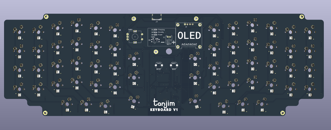
Routed the PCB

This took 2 days. It got harder as I went and the board started becoming more and more cluttered, at some point my ground pours and power pours started fragmenting even, fixing that was a pain. And I still have to fix 612 DRC violations. help

tanjim
added to the journal ago
Added the edge and flipped most components to the other side

I added the edge of the PCB, which was a bit hard because of weird KiCad stuff (not thr 720p this time) and rounded it. I also flipped most components to the other side since I will not be using a case (only a second bottomplate PCB mounted using standoffs as protection) and many tiny components can look a bit ugly. I kept these on the top side for obvious reasons:
- Rotary encoder
- BOOT,RESET buttons
- Charging,Power,Standby LEDs
- OLED screen
I also added the mounting holes.


tanjim
added to the journal ago
Designed this logo thing


I used inkscape to make this logo. Here's how it looks in the PCB

Since I am not going to use a case for this I will use another PCB shaped the same way thats mounted below it with hex standoffs (kind of like raspberry pi HATs). I can put a larger logo there, since it wont have any electric components.
tanjim
added to the journal ago
Arranged the PCB components

This took a lot of time since:
- (again) i only have a 720p screen
- arranging the power circuit was tough (this is wireless!)
- deciding on the exact layout was also hard, like I have to make sure this feels good to use
tanjim
added to the journal ago
created the PCB grid
i created the grid of keys in the PCB

instead of dragging each diode and LED into each key manually I decided to use a plugin that does that for me. however, the grid was not produced correctly by the plugin. however, by noticing that even though the grid is not a rectangle yet, neither is the order correct, every switch number in the same vertical column was in the same residue class modulo 12 (\forall\text{column} A,\forall \text{keyswitch num} x,y \in A, x \equiv y (\text{mod} 12)), so i was able to find a way to turn it into the correct grid
(edit 1: just realized this does not support full markdown so that is not formatted)
(edit 2: this doesnt even support strikethrough i can't even strikethrough the unformatted text
tanjim
added to the journal ago
Added LCSC part numbers
I added LCSC part numbers so JLCPCB can do PCBA.

i had to go on LCSC and click the filters until i found the part since LCSC has this weird search where searching something like diode or AP2112K wont work.
tanjim
added to the journal ago
added RGB + fixed the schematic
i literally forgot about RGB/backlights the first time through

here is what I did:
- added SK6812 Mini-E LEDs

- a polyfuse just incase i short out power or I accidentally turn on the LEDs at 100%

- this power LED was polarity reversed i fixed that

- had to increase the schematic (not pcb) size from the initial A4 to A3 to now A2 (4x increase)

tanjim
added to the journal ago
Downloaded every single footprint needed and...
Downloaded every single footprint needed and assigned them to the symbols. Self explanatory.
I had to spend 30 minutes digging around for footprint libraries, then had to spend another 30 after realizing I downloaded the symbols again accidentally, then I had to look at the list and figure out which one of the components was right, like its impossible to guess what something like Rotary_Encoder:RotaryEncoder_Alps_EC11E-Switch_Vertical_H20mm is supposed to mean without 10 minutes of research. Multiply that by the ~10 options per component and ~30 components and you get justification for why this step took 2 hours.

(note: you may see the upload times and say i am frauding, no i am not because i thought this was a hackpad for the first few hours and it said "journal not needed" now i realized that this is not a hackpad and i am writing the journals)
tanjim
added to the journal ago
Made the schematic

it was much harder than it looks because
- its my first PCB
- i have only a 720p screen which is very annoying for this, like zoom out a bit and text turns into unreadable blobs, like try zooming into that screenshot and reading the tiny text its impossible
- kicad crashed
tanjim
added to the journal ago
decide on the keyboard layout, switches
I decided to go with a split lily58 monoblock style keyboard layout (not exactly but this is what I will build off.
Here's how the lily58 layout looks:

(NONE OF THE IMAGES ARE MY KEYBOARD! i just put this image to show the approximate layout)
here is a sloppy drawing of what the keyboard layout will look like (there are two extra keys)

Ofcouse, I didnt just land on this decision instantly. These are what I considered:
- Sofle This is very similar to the Lily58 layout. Since I am not copy-pasting the design (doing it by hand) it will technically be both and neither sofle and lily58.
- Atreus62 I also dont know the difference with this from lily58 and sofle.
- Lumberjack this ones completely ortholinear with no thumb cluster, its just the Preonic layout except spaced apart.

-
Preonic Ortholinear and non split.

Time estimate: 1.75 hrs
tanjim
started split keyboard (layout: lily58-like monoblock) ago
1/2/2026 4 PM - decide on the keyboard layout, switches
I decided to go with a split lily58 monoblock style keyboard layout (not exactly but this is what I will build off.
Here's how the lily58 layout looks:
(NONE OF THE IMAGES ARE MY KEYBOARD! i just put this image to show the approximate layout)
here is a sloppy drawing of what the keyboard layout will look like (there are two extra keys)
Ofcouse, I didnt just land on this decision instantly. These are what I considered:
- Sofle This is very similar to the Lily58 layout. Since I am not copy-pasting the design (doing it by hand) it will technically be both and neither sofle and lily58.
- Atreus62 I also dont know the difference with this from lily58 and sofle.
- Lumberjack this ones completely ortholinear with no thumb cluster, its just the Preonic layout except spaced apart.
-
Preonic Ortholinear and non split.
Time estimate: 1.75 hrs
1/2/2026 5:26 PM - Made the schematic
it was much harder than it looks because
- its my first PCB
- i have only a 720p screen which is very annoying for this, like zoom out a bit and text turns into unreadable blobs, like try zooming into that screenshot and reading the tiny text its impossible
- kicad crashed
1/2/2026 5:32 PM - Downloaded every single footprint needed and...
Downloaded every single footprint needed and assigned them to the symbols. Self explanatory.
I had to spend 30 minutes digging around for footprint libraries, then had to spend another 30 after realizing I downloaded the symbols again accidentally, then I had to look at the list and figure out which one of the components was right, like its impossible to guess what something like Rotary_Encoder:RotaryEncoder_Alps_EC11E-Switch_Vertical_H20mm is supposed to mean without 10 minutes of research. Multiply that by the ~10 options per component and ~30 components and you get justification for why this step took 2 hours.
(note: you may see the upload times and say i am frauding, no i am not because i thought this was a hackpad for the first few hours and it said "journal not needed" now i realized that this is not a hackpad and i am writing the journals)
1/2/2026 6 PM - added RGB + fixed the schematic
i literally forgot about RGB/backlights the first time through
here is what I did:
- added SK6812 Mini-E LEDs
- a polyfuse just incase i short out power or I accidentally turn on the LEDs at 100%
- this power LED was polarity reversed i fixed that
- had to increase the schematic (not pcb) size from the initial A4 to A3 to now A2 (4x increase)
1/2/2026 8 PM - Added LCSC part numbers
I added LCSC part numbers so JLCPCB can do PCBA.
i had to go on LCSC and click the filters until i found the part since LCSC has this weird search where searching something like diode or AP2112K wont work.
1/2/2026 10 PM - created the PCB grid
i created the grid of keys in the PCB
instead of dragging each diode and LED into each key manually I decided to use a plugin that does that for me. however, the grid was not produced correctly by the plugin. however, by noticing that even though the grid is not a rectangle yet, neither is the order correct, every switch number in the same vertical column was in the same residue class modulo 12 (\forall\text{column} A,\forall \text{keyswitch num} x,y \in A, x \equiv y (\text{mod} 12)), so i was able to find a way to turn it into the correct grid
(edit 1: just realized this does not support full markdown so that is not formatted)
(edit 2: this doesnt even support strikethrough i can't even strikethrough the unformatted text
1/4/2026 2 PM - Arranged the PCB components
This took a lot of time since:
- (again) i only have a 720p screen
- arranging the power circuit was tough (this is wireless!)
- deciding on the exact layout was also hard, like I have to make sure this feels good to use
1/4/2026 4 PM - Designed this logo thing
I used inkscape to make this logo. Here's how it looks in the PCB
Since I am not going to use a case for this I will use another PCB shaped the same way thats mounted below it with hex standoffs (kind of like raspberry pi HATs). I can put a larger logo there, since it wont have any electric components.
1/4/2026 8 PM - Added the edge and flipped most components to the other side
I added the edge of the PCB, which was a bit hard because of weird KiCad stuff (not thr 720p this time) and rounded it. I also flipped most components to the other side since I will not be using a case (only a second bottomplate PCB mounted using standoffs as protection) and many tiny components can look a bit ugly. I kept these on the top side for obvious reasons:
- Rotary encoder
- BOOT,RESET buttons
- Charging,Power,Standby LEDs
- OLED screen
I also added the mounting holes.
1/6/2026 - Routed the PCB
This took 2 days. It got harder as I went and the board started becoming more and more cluttered, at some point my ground pours and power pours started fragmenting even, fixing that was a pain. And I still have to fix 612 DRC violations. help
1/7/2026 - Made the bottom plate PCB
This is going to be mounted under the main keyboard with standoffs for protection (like i dont want my keyboard to short itself when I put it on the table). The battery will also be between the two PCBs.
1/8/2026 8 PM - help
i just found that all kalih choc hotswap switch sockets and switches are out of stock so I have to switch to cherry MX. this means I have to redo the ENTIRE PCB AGAIN.
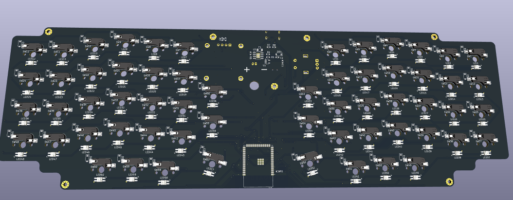
1/8/2026 10 PM - arranged the keyboard grid for the 2nd time
same thing as before except its cherry mx (19.05mm grid instead of 18x17) and I made it a little more intelligently than before so my wires are less messy.
1/9/2026 2 PM - Routed the key matrix for the 2nd time
this one was a lot easier because I was able to use the improved grid plus cherry switches are biggerr than choc switches and now routing a trace did not feel like an aadvanced math problem
comparision
before
after
1/9/2026 5 PM - Completed the PCB for the second time!
the power circuit was still a nightmare to route even though the keyboard matrix was easier. now its jlcpcb time!