 Kai the Jolly Guy 🚀
rejected Rasp_IO_board with NVME ago
Kai the Jolly Guy 🚀
rejected Rasp_IO_board with NVME ago
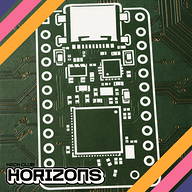
Please don't fraud a nonprofit, your project is a 1 to 1 replica of the CM5 IO board :(
 Prince
submitted Rasp_IO_board with NVME for ship review ago
Prince
submitted Rasp_IO_board with NVME for ship review ago
 PenguinMo
requested changes for Rasp_IO_board with NVME ago
PenguinMo
requested changes for Rasp_IO_board with NVME ago
your cart screenshots and grant request don't match
Prince
submitted Rasp_IO_board with NVME for ship review ago
Prince
added to the journal ago
Update
As suggested, i am not including the CM5 module in the cost sheet and also i would like bring to yout notice that i would pay the shipping the cost for the pcb from my own.. i require funding only for the pcb and only the components of 2 PCB's not all 5... in total i require funding 32.60$ for the pcb and 57.80$ for the components totalling 86.73$


 samliu ⚡🚀
requested changes for Rasp_IO_board with NVME ago
samliu ⚡🚀
requested changes for Rasp_IO_board with NVME ago
Unfortunately this project doesn't qualify for Tier 1. You're using a very expensive part that is designed by someone else. We won't be able to fund it with the CM5 as I can't see the direct need for it.
Prince
submitted Rasp_IO_board with NVME for ship review ago
 technical_.
requested changes for Rasp_IO_board with NVME ago
technical_.
requested changes for Rasp_IO_board with NVME ago
Please break up your journal into smaller hour bits. I cannot understand your journal.
Prince
submitted Rasp_IO_board with NVME for ship review ago
Prince
added to the journal ago
Cost sheet
The total project costs around 300$... all the parts are sourced from jlcpcb adn robu.in .. the pcb is sourced from jlcpcb.. i have the choosen the cheaest shipping


Prince
added to the journal ago
Full jornul
Day 1 – 6 hrs
Today was focused entirely on understanding what kind of project I was actually trying to build and why it should exist in the first place. I did not open any schematic or PCB software today. Instead, I spent time thinking about the limitations of typical Raspberry Pi expansion boards and why most of them fail to expose real system-level design challenges. I realized that most boards only break out GPIO or add a single peripheral, which avoids dealing with signal integrity, power stability, and interface coexistence.
I decided early that this board should not be treated as a passive adapter. The goal was to design a system-level I/O board that integrates PCIe NVMe storage along with USB 3.x, HDMI, Ethernet, GPIO, SDCard, and USB-C power input on a single PCB. This immediately framed the project as a high-complexity design involving both high-speed and low-speed domains. I spent time defining the core problem as how to safely, reliably, and manufacturably expand a Raspberry Pi using PCIe NVMe while also supporting multiple sensitive interfaces without electrical interference.
A significant portion of the time was spent identifying why this problem is non-trivial. PCIe requires tightly controlled differential routing and stable reference planes, NVMe drives draw large transient currents, USB-C power inputs require protection and discharge handling, and USB 3.x and HDMI signals are highly sensitive to noise. At the same time, low-speed GPIO and SDCard signals must remain isolated from these high-speed domains. Understanding that all of these constraints must be satisfied simultaneously on one board helped me realize the seriousness of the design challenge.
By the end of the day, I had clearly defined the functional goals of the board, including NVMe support via PCIe, USB-C power input with protection, USB 3.x, HDMI, Ethernet, GPIO, and SDCard interfaces. I also defined non-functional goals such as schematic clarity, conservative electrical margins, manufacturability, and debug accessibility. This day established the design philosophy of prioritizing stability and clarity over compactness and set expectations for a structured, multi-phase design process going forward.
Day 2 – 6 hrs
Today I focused on turning the abstract project idea into a set of concrete requirements that could guide the design in a controlled way. Rather than jumping straight into schematics, I spent time clearly defining what the board must do and what it should explicitly avoid doing. This helped prevent scope creep and kept the project aligned with its original learning goals.
I defined the core functional requirements of the board, including support for an M.2 NVMe SSD through PCIe, correct interfacing with the Raspberry Pi PCIe lanes, USB-C power input with proper protection, USB 3.x high-speed signaling, HDMI output, Ethernet connectivity, GPIO expansion, and SDCard support. Each requirement was considered in terms of electrical feasibility and interaction with other interfaces rather than as an isolated feature.
In parallel, I defined non-functional design goals that would heavily influence later decisions. These included maintaining a clear schematic hierarchy, logical separation of high-speed and low-speed circuits, conservative electrical margins, manufacturability using standard PCB processes, and accessibility for debugging during bring-up. I intentionally avoided optimizing for minimum board size or extreme trace density, as reliability and clarity were higher priorities for this project.
A significant portion of the day was spent studying background material related to the interfaces involved. I reviewed PCIe routing guidelines, NVMe power behavior, USB-C current handling and discharge requirements, USB 3.x and HDMI differential pair constraints, and Raspberry Pi PCIe documentation. This research shaped how I began to mentally organize the board, especially with respect to connector placement and power filtering strategies.
By the end of the day, I had clearly identified which signals belonged to high-speed domains such as PCIe, USB 3.x, and HDMI, and which belonged to low-speed domains like GPIO, SDCard, control signals, and indicators. This separation became a foundational principle for the schematic organization and PCB layout that would follow. The day concluded with a clear understanding of the constraints involved and a structured direction for moving into architectural planning.
Day 3 – 7 hrs
Today was focused on translating the previously defined requirements and constraints into a high-level system architecture. I did not yet begin detailed schematic capture, but instead concentrated on how the board should be logically structured to remain understandable and manageable as complexity increased. This involved thinking about the design in terms of functional blocks rather than individual components.
I began by partitioning the board into distinct architectural blocks, including a PCIe to M.2 NVMe block, a USB-C power input and protection block, a high-speed serial I/O block for USB 3.x and HDMI, a GPIO, Ethernet, and SDCard block, and a dedicated power regulation and filtering block. Each block was intended to be as self-contained as possible, with clean and minimal interfaces between them.
A significant part of the day was spent deciding how these blocks should interact electrically without interfering with each other. I paid particular attention to how high-speed domains such as PCIe, USB 3.x, and HDMI would be isolated from low-speed signals and control lines. This separation was not only conceptual but was also planned to be reflected later in schematic organization, component placement, and routing strategy.
Power integrity was treated as a first-class architectural concern during this stage. I considered worst-case scenarios such as NVMe inrush current, transient load behavior, and USB-C power source variability. Rather than assuming ideal power conditions, I planned the architecture around conservative assumptions, ensuring that noisy and sensitive power paths could be separated and filtered appropriately.
By the end of the day, I had a clear architectural roadmap for the entire project. The schematic would be organized into multiple dedicated sheets aligned with the defined blocks, and future phases were planned in a structured sequence covering schematic design, placement, routing, verification, and bring-up. This day effectively marked the transition from abstract planning into executable design work.
Day 4 – 7 hrs
Today marked the transition from system-level planning into actual schematic preparation. Before placing any components, I revisited the architectural blocks defined earlier and reviewed them with a schematic-oriented mindset. The goal was to ensure that each block could be translated into a clean, readable schematic sheet without excessive cross-connections or ambiguity.
I finalized the strategy of using multiple schematic sheets instead of a single monolithic schematic. Each sheet would focus on a specific subsystem, such as PCIe to NVMe, USB-C power input, high-speed serial I/O, GPIO and Ethernet, and power regulation. This decision was made to reduce cognitive load during both design and review, and to make debugging easier later in the project.
A significant portion of the day was spent planning how signals would cross between schematic sheets. I carefully considered which signals should remain local to a block and which needed to be shared globally. This was especially important for high-speed interfaces and power rails, where unclear net naming or accidental duplication could create serious problems during layout.
I also began preparing for detailed schematic capture by reviewing datasheets more closely with implementation in mind. This included checking pin functions, power requirements, configuration pins, and reference design recommendations for key interfaces. Rather than copying reference designs blindly, I focused on understanding why certain components and connections were required.
By the end of the day, the schematic structure was clearly defined and ready for execution. The overall system architecture, power strategy, and domain separation were locked in conceptually, allowing the project to move confidently into detailed schematic design starting with the PCIe to M.2 NVMe subsystem.
Day 5 – 7 hrs
Today was focused on beginning detailed schematic capture, starting with the most critical subsystem of the entire board: the PCIe to M.2 NVMe interface. I intentionally chose to work on this block first because it defines the core functionality of the project and imposes the strongest constraints on routing, power integrity, and layout.
I carefully mapped the Raspberry Pi PCIe signals to the M.2 connector pins, paying close attention to transmit and receive differential pairs, polarity, reference clock routing, reset signals, and wake functionality. I verified each connection against both the Raspberry Pi PCIe documentation and the M.2 NVMe specification to ensure correctness and avoid subtle compatibility issues that could be difficult to debug later.
A significant portion of the time was spent understanding and implementing the power requirements for NVMe drives. NVMe devices can draw large transient currents, especially during initialization, so I treated the NVMe power rail as a high-demand domain rather than a simple extension of an existing supply. I added dedicated power filtering, bulk capacitance near the M.2 connector, and local decoupling capacitors placed close to the power pins.
Rather than relying on assumptions, I reviewed NVMe power behavior and reference designs to understand how similar systems handle startup current spikes and noise sensitivity. This influenced how aggressively power filtering was applied and reinforced the need for a stable and low-impedance supply path to the NVMe socket.
By the end of the day, the PCIe to M.2 NVMe schematic block was largely complete and internally consistent. This established a solid electrical foundation for the rest of the design and allowed me to move forward with confidence into other schematic subsystems without risking fundamental flaws in the core interface.
Day 6 – 6 hrs
Today was focused on designing the USB-C power input subsystem, with particular attention to safety, robustness, and real-world behavior. Because USB-C is capable of delivering significant power and can behave unpredictably if not handled correctly, I treated this block as a critical subsystem rather than a simple connector.
I worked on the USB-C configuration and CC pin handling, adding the required resistors for proper cable orientation detection and ensuring that discharge paths were present to safely bleed residual charge after disconnect. I also paid attention to how the connector shield and shell were grounded to provide a low-impedance path for noise and improve EMI behavior.
Current limiting and protection circuitry were included to protect both the board and the power source from fault conditions or excessive inrush current. Instead of assuming an ideal power supply, I designed the input stage to tolerate a range of real-world USB-C power sources and connection scenarios.
Throughout the process, I referenced established USB-C design guidelines and compared my schematic choices against known-good implementations. This helped confirm that the board would behave safely during plug-in, operation, and unplug events without relying on undocumented behavior.
By the end of the day, the USB-C power input and protection block was complete and integrated cleanly into the overall schematic structure. This provided a stable and safe entry point for power into the board and allowed me to proceed with confidence to the remaining high-speed interface schematics.
Day 7 – 7 hrs
Today was focused on completing the remaining high-speed serial interface schematics, specifically USB 3.x and HDMI. These interfaces were treated as electrically sensitive subsystems rather than simple connectors, and I approached their schematic design with the expectation that routing and grounding decisions later would depend heavily on the choices made here.
For the USB 3.x interface, I implemented the SuperSpeed differential pairs with careful attention to signal integrity requirements. I ensured that the schematic avoided unnecessary components in the signal path and that grounding references and shield connections were clearly defined. The goal was to preserve signal quality and avoid introducing avoidable sources of impedance discontinuity or noise coupling.
The HDMI schematic block was designed next. This included the TMDS differential pairs, associated control and I²C lines, and hot-plug detect signals. I paid special attention to grounding and reference signals, knowing that HDMI is particularly sensitive to noise and poor return paths. Control signals were kept logically separate from the high-speed TMDS pairs to maintain clarity.
Throughout the day, I continuously reviewed how these high-speed blocks interacted with previously designed subsystems. I reinforced the separation between high-speed domains such as PCIe, USB 3.x, and HDMI and low-speed signals like GPIO, LEDs, and configuration lines. This separation was reflected in schematic grouping and net naming to reduce the risk of accidental coupling later.
By the end of the day, all major high-speed interface schematics were complete and internally consistent. With PCIe, USB 3.x, HDMI, and USB-C power blocks defined, the schematic now represented the full set of critical interfaces and was ready to be expanded with remaining low-speed connectivity and final power distribution details.
Day 8 – 6 hrs
Today was focused on completing the remaining low-speed and supporting schematic blocks and preparing the entire schematic for review and lockdown. With all major high-speed interfaces already defined, the emphasis shifted toward integrating GPIO, Ethernet, SDCard, and power distribution in a way that preserved clarity and avoided interference with sensitive domains.
I worked on the GPIO expansion circuitry, grouping pins logically and labeling them clearly to reduce confusion during later use and debugging. Where appropriate, voltage references and basic protection were included to ensure predictable behavior. The Ethernet interface was also completed, with attention paid to differential pair handling, grounding, and magnetics considerations. Although Ethernet operates at high speeds, it was treated separately from PCIe and USB due to its different signaling characteristics.
The SDCard interface was designed with a focus on clean power and short, direct signal paths. Pull-up resistors and power connections were reviewed to ensure stable operation. I intentionally placed this interface in a conceptual quiet zone to minimize the influence of nearby high-speed activity.
Power distribution across the board was reviewed and finalized. Instead of relying on a single monolithic power rail, I implemented a distributed power strategy with local filtering and decoupling for each major subsystem. Clear and consistent net naming was used to reduce ambiguity and simplify later layout and verification.
By the end of the day, I performed a full cross-sheet schematic review. I verified that all high-speed nets connected correctly, that power rails were consistent across sheets, and that no unintended signal splits or omissions existed. With this review complete, the schematic was considered locked, allowing the project to transition confidently into component placement and physical layout.
Day 9 – 7 hrs
Today marked the transition from schematic design into physical PCB layout work. Before placing any components, I focused entirely on verifying footprints, especially for components that would be difficult or impossible to rework if incorrect. I treated footprint validation as a critical risk-reduction step rather than an optional check.
I reviewed each high-risk footprint in detail, comparing library definitions against manufacturer datasheets. This included verifying pin numbering, pin one orientation, pad sizes, pad shapes, mechanical outlines, and keep-out areas. Special attention was given to connectors and sockets, where even small mistakes can render a board unusable.
Extra care was taken with the M.2 NVMe socket, USB-C connector, HDMI connectors, USB 3.x connectors, Ethernet connector and magnetics, and high-pin-count headers. For each of these, I cross-checked the footprint against the datasheet rather than relying on assumptions or generic library symbols. This process consumed significant time but was necessary to reduce fabrication risk.
As part of this verification pass, I also reviewed connector shell and shield pin handling to ensure proper grounding and mechanical stability. This was especially important for high-speed and high-current connectors where poor grounding can lead to EMI or reliability issues.
By the end of the day, all critical footprints were verified and corrected where necessary. With confidence in the physical accuracy of the components, the project was ready to move forward into deliberate component placement without risking avoidable mechanical or assembly errors.
Day 10 – 7 hrs
Today was focused on the initial and most critical phase of component placement. Because placement directly affects routing feasibility, signal integrity, and EMI behavior, I approached this step as an electrical design task rather than a cosmetic one. I began by reviewing the schematic again with placement priorities in mind.
The first component placed was the M.2 NVMe socket, as it imposes the strongest constraints on the entire board. I positioned the socket as close as possible to the Raspberry Pi PCIe source to minimize differential pair length and avoid unnecessary vias or layer transitions. The orientation was chosen to allow straight and symmetrical routing of PCIe transmit and receive pairs.
In addition to electrical considerations, I accounted for mechanical constraints related to the NVMe module, including mounting hole alignment, clearance for different module lengths, and accessibility for installation and removal. Balancing these electrical and mechanical factors required several small adjustments before the socket position was finalized.
After finalizing the NVMe socket position, I placed the USB-C power connector near the board edge to allow easy cable insertion and reduce mechanical stress. This placement also helped keep high-current power paths short and isolated from sensitive signal routing areas.
By the end of the day, the most critical components defining board geometry and high-speed routing corridors were placed deliberately. This established a strong foundation for placing remaining components and significantly reduced routing complexity in later stages.
Day 11 – 6 hrs
Today was focused on completing the remaining component placement and refining the overall physical layout of the board. With the most critical high-speed connectors already placed, I shifted attention to power regulation components and low-speed interfaces, ensuring they were positioned in a way that supported clean routing and minimal interference.
Power regulation components, including regulators, inductors, bulk capacitors, and associated resistors, were grouped into a dedicated zone. This grouping allowed for short power loops, improved EMI containment, and clear separation from high-speed routing corridors. I intentionally kept switching power components away from PCIe, USB 3.x, and HDMI signal paths.
GPIO headers were placed with mechanical accessibility and clarity in mind. I ensured that headers were oriented consistently, labeled clearly, and located away from high-speed differential pairs. This improves usability and reduces the risk of accidental interference during debugging or external connections.
Ethernet and SDCard components were placed next. Although Ethernet uses differential signaling, it was treated separately from PCIe and USB due to transformer isolation and different signaling characteristics. The SDCard circuitry was placed in a quieter region of the board with short signal paths and clean power.
By the end of the day, I performed an initial placement review, checking spacing, board edge clearances, silkscreen readability, and mechanical alignment. With placement reaching a stable and electrically sensible state, component placement was considered complete and ready to be locked before routing.
Day 12 – 8 hrs
Today marked the transition from component placement into actual PCB routing. Before routing any signals, I focused on defining routing priorities and establishing a disciplined order of operations. Given the number of high-speed interfaces on the board, I did not want routing decisions to be driven by convenience or leftover space.
I began by routing power first, as power integrity defines current return paths and heavily influences signal routing quality. Wide copper pours were used for major power rails instead of thin traces to reduce impedance and voltage drop, especially for high-load domains such as the NVMe power rail. This step helped prevent later signal routes from blocking critical power paths.
Alongside power routing, I focused on ground plane strategy. Rather than aggressively splitting ground, I aimed to preserve a continuous ground reference wherever possible. High-speed differential pairs were planned to always route over a solid ground plane to maintain predictable impedance and clean return paths.
Stitching vias were added near high-speed connectors, around the NVMe socket, and near power filtering components. These vias help reduce ground impedance and improve EMI performance, especially in areas where signals transition between layers or enter the board from connectors.
By the end of the day, the core power distribution and ground reference structure of the board were in place. This created a stable electrical foundation that allowed high-speed signal routing to proceed in a controlled and predictable manner during subsequent routing sessions.
Day 13 – 8 hrs
Today was dedicated to routing the most electrically demanding interfaces on the board: PCIe for the NVMe interface and USB 3.x SuperSpeed signals. Because these interfaces operate at multi-gigabit speeds, routing decisions made here directly determine whether the board will function reliably.
I started with PCIe differential pair routing between the Raspberry Pi PCIe source and the M.2 NVMe socket. I followed strict constraints, including controlled impedance routing, tight length matching within each differential pair, minimal via usage, and smooth trace geometry without sharp corners. I avoided unnecessary layer changes to reduce impedance discontinuities and preserve signal quality.
The first PCIe routing attempt revealed congestion near the NVMe socket. Rather than forcing the routes, I stepped back and adjusted nearby signal paths to create a cleaner routing corridor. This iterative approach improved symmetry between differential pairs and reduced routing stress, even though it required rework.
After completing PCIe routing, I moved on to USB 3.x SuperSpeed pairs. These were routed with equal care, maintaining consistent spacing and length matching within each pair while keeping them isolated from noisy power paths and switching regulators. I accepted slightly longer routes when it improved isolation and reduced the risk of crosstalk.
By the end of the day, both PCIe and USB 3.x high-speed routes were complete and visually clean. These routes respected return path continuity and left sufficient clearance from other signals, setting a strong foundation for routing the remaining high-speed interfaces.
Day 14 – 6 hrs
Today was focused on completing the remaining routing tasks and refining the overall layout. With PCIe and USB 3.x already routed, I moved on to HDMI differential pairs, Ethernet signals, and finally the low-speed control and GPIO routing. This order ensured that the most sensitive signals were not constrained by earlier routing decisions.
HDMI routing required careful attention due to the number of TMDS differential pairs involved. I routed these pairs as tightly coupled differential traces, prioritized length consistency, and kept control and I²C signals separate from the high-speed TMDS lanes. I avoided routing HDMI pairs near power components or parallel to USB SuperSpeed paths to minimize interference.
Ethernet differential pairs were routed next. Although Ethernet is more tolerant due to transformer isolation, I still ensured clean differential routing and maintained continuous return paths. Care was taken to minimize crosstalk with nearby high-speed interfaces and preserve signal integrity.
Low-speed signals such as GPIO, LEDs, SDCard, and control lines were routed last. These signals were allowed to take longer or more complex paths where necessary, as their timing requirements are less strict. Routing them last helped keep high-speed paths clean and direct.
By the end of the day, I performed an EMI and routing cleanup pass. This included removing unnecessary vias, smoothing awkward trace bends, reviewing parallel routing risks, and ensuring return path continuity. With these refinements complete, routing was considered finished and ready for formal verification.
Day 15 – 6 hrs
Today was dedicated entirely to verification and validation of the completed design. Although the board appeared complete after routing, I intentionally paused all layout changes and shifted focus from building to systematically checking correctness, safety, and manufacturability. This phase was treated as a critical engineering task rather than a formality.
I began by running Electrical Rule Checks on the schematic to identify any logical issues such as unconnected pins, conflicting pin types, or improperly defined power connections. Several warnings appeared during the first pass, including unused GPIO pins and configuration pins relying on internal pull-ups. Rather than ignoring these, I reviewed the relevant datasheets and added explicit pull-up or pull-down resistors where appropriate to improve robustness.
After resolving schematic-level concerns, I moved on to PCB-level Design Rule Checks. The initial DRC pass revealed minor clearance violations, silkscreen overlaps, and a few unconnected nets. Each issue was addressed methodically by adjusting trace spacing, relocating reference designators, or completing missing connections. DRC was re-run repeatedly until the board passed without errors.
In addition to automated checks, I performed a manual review of all high-speed routing. PCIe, USB 3.x, and HDMI differential pairs were inspected for continuity, spacing consistency, via usage, and ground reference integrity. Any questionable routing segments were corrected, even if it required sacrificing some layout compactness.
By the end of the day, I validated footprint orientation and connector alignment one final time and generated manufacturing outputs including Gerber and drill files. These files were reviewed using a Gerber viewer to ensure they accurately represented the final design. With all checks complete, the board was considered fabrication-ready.
Day 16 – 6 hrs
Today was focused on preparing the design for real-world use and documenting how the board would be safely powered, tested, and validated once fabricated. Rather than modifying the design further, the emphasis was on planning a structured bring-up process and defining what successful operation would look like for each subsystem.
I outlined a step-by-step bring-up strategy to reduce risk during first power-on. This included visual inspection of assembly quality, continuity and short-circuit testing, and controlled power-up without the NVMe module installed. Special attention was given to validating USB-C power behavior, monitoring current draw, and confirming stable voltage rails before enabling higher-load subsystems.
I then documented a progressive interface validation plan, starting with low-speed GPIO and SDCard interfaces, followed by Ethernet, and finally high-speed interfaces such as USB 3.x, HDMI, and PCIe NVMe. This staged approach helps isolate issues and avoids compounding failures during early testing.
Performance expectations and validation criteria were clearly defined for each subsystem. Rather than targeting peak theoretical performance, the focus was on reliable enumeration, stable operation across power cycles, and predictable behavior under load. Any critical deviations such as link instability, excessive power droop, or unexplained resets were identified as triggers for further investigation or design revision.
By the end of the day, I reflected on the overall project and documented key lessons learned, including the importance of disciplined high-speed design, careful placement, power integrity, and thorough verification. The project was considered complete and fabrication-ready, with clear plans for testing, iteration, and future improvement based on measured behavior rather than assumptions.


Prince
started Rasp_IO_board with NVME ago
1/4/2026 7 PM - Full jornul
Day 1 – 6 hrs
Today was focused entirely on understanding what kind of project I was actually trying to build and why it should exist in the first place. I did not open any schematic or PCB software today. Instead, I spent time thinking about the limitations of typical Raspberry Pi expansion boards and why most of them fail to expose real system-level design challenges. I realized that most boards only break out GPIO or add a single peripheral, which avoids dealing with signal integrity, power stability, and interface coexistence.
I decided early that this board should not be treated as a passive adapter. The goal was to design a system-level I/O board that integrates PCIe NVMe storage along with USB 3.x, HDMI, Ethernet, GPIO, SDCard, and USB-C power input on a single PCB. This immediately framed the project as a high-complexity design involving both high-speed and low-speed domains. I spent time defining the core problem as how to safely, reliably, and manufacturably expand a Raspberry Pi using PCIe NVMe while also supporting multiple sensitive interfaces without electrical interference.
A significant portion of the time was spent identifying why this problem is non-trivial. PCIe requires tightly controlled differential routing and stable reference planes, NVMe drives draw large transient currents, USB-C power inputs require protection and discharge handling, and USB 3.x and HDMI signals are highly sensitive to noise. At the same time, low-speed GPIO and SDCard signals must remain isolated from these high-speed domains. Understanding that all of these constraints must be satisfied simultaneously on one board helped me realize the seriousness of the design challenge.
By the end of the day, I had clearly defined the functional goals of the board, including NVMe support via PCIe, USB-C power input with protection, USB 3.x, HDMI, Ethernet, GPIO, and SDCard interfaces. I also defined non-functional goals such as schematic clarity, conservative electrical margins, manufacturability, and debug accessibility. This day established the design philosophy of prioritizing stability and clarity over compactness and set expectations for a structured, multi-phase design process going forward.
Day 2 – 6 hrs
Today I focused on turning the abstract project idea into a set of concrete requirements that could guide the design in a controlled way. Rather than jumping straight into schematics, I spent time clearly defining what the board must do and what it should explicitly avoid doing. This helped prevent scope creep and kept the project aligned with its original learning goals.
I defined the core functional requirements of the board, including support for an M.2 NVMe SSD through PCIe, correct interfacing with the Raspberry Pi PCIe lanes, USB-C power input with proper protection, USB 3.x high-speed signaling, HDMI output, Ethernet connectivity, GPIO expansion, and SDCard support. Each requirement was considered in terms of electrical feasibility and interaction with other interfaces rather than as an isolated feature.
In parallel, I defined non-functional design goals that would heavily influence later decisions. These included maintaining a clear schematic hierarchy, logical separation of high-speed and low-speed circuits, conservative electrical margins, manufacturability using standard PCB processes, and accessibility for debugging during bring-up. I intentionally avoided optimizing for minimum board size or extreme trace density, as reliability and clarity were higher priorities for this project.
A significant portion of the day was spent studying background material related to the interfaces involved. I reviewed PCIe routing guidelines, NVMe power behavior, USB-C current handling and discharge requirements, USB 3.x and HDMI differential pair constraints, and Raspberry Pi PCIe documentation. This research shaped how I began to mentally organize the board, especially with respect to connector placement and power filtering strategies.
By the end of the day, I had clearly identified which signals belonged to high-speed domains such as PCIe, USB 3.x, and HDMI, and which belonged to low-speed domains like GPIO, SDCard, control signals, and indicators. This separation became a foundational principle for the schematic organization and PCB layout that would follow. The day concluded with a clear understanding of the constraints involved and a structured direction for moving into architectural planning.
Day 3 – 7 hrs
Today was focused on translating the previously defined requirements and constraints into a high-level system architecture. I did not yet begin detailed schematic capture, but instead concentrated on how the board should be logically structured to remain understandable and manageable as complexity increased. This involved thinking about the design in terms of functional blocks rather than individual components.
I began by partitioning the board into distinct architectural blocks, including a PCIe to M.2 NVMe block, a USB-C power input and protection block, a high-speed serial I/O block for USB 3.x and HDMI, a GPIO, Ethernet, and SDCard block, and a dedicated power regulation and filtering block. Each block was intended to be as self-contained as possible, with clean and minimal interfaces between them.
A significant part of the day was spent deciding how these blocks should interact electrically without interfering with each other. I paid particular attention to how high-speed domains such as PCIe, USB 3.x, and HDMI would be isolated from low-speed signals and control lines. This separation was not only conceptual but was also planned to be reflected later in schematic organization, component placement, and routing strategy.
Power integrity was treated as a first-class architectural concern during this stage. I considered worst-case scenarios such as NVMe inrush current, transient load behavior, and USB-C power source variability. Rather than assuming ideal power conditions, I planned the architecture around conservative assumptions, ensuring that noisy and sensitive power paths could be separated and filtered appropriately.
By the end of the day, I had a clear architectural roadmap for the entire project. The schematic would be organized into multiple dedicated sheets aligned with the defined blocks, and future phases were planned in a structured sequence covering schematic design, placement, routing, verification, and bring-up. This day effectively marked the transition from abstract planning into executable design work.
Day 4 – 7 hrs
Today marked the transition from system-level planning into actual schematic preparation. Before placing any components, I revisited the architectural blocks defined earlier and reviewed them with a schematic-oriented mindset. The goal was to ensure that each block could be translated into a clean, readable schematic sheet without excessive cross-connections or ambiguity.
I finalized the strategy of using multiple schematic sheets instead of a single monolithic schematic. Each sheet would focus on a specific subsystem, such as PCIe to NVMe, USB-C power input, high-speed serial I/O, GPIO and Ethernet, and power regulation. This decision was made to reduce cognitive load during both design and review, and to make debugging easier later in the project.
A significant portion of the day was spent planning how signals would cross between schematic sheets. I carefully considered which signals should remain local to a block and which needed to be shared globally. This was especially important for high-speed interfaces and power rails, where unclear net naming or accidental duplication could create serious problems during layout.
I also began preparing for detailed schematic capture by reviewing datasheets more closely with implementation in mind. This included checking pin functions, power requirements, configuration pins, and reference design recommendations for key interfaces. Rather than copying reference designs blindly, I focused on understanding why certain components and connections were required.
By the end of the day, the schematic structure was clearly defined and ready for execution. The overall system architecture, power strategy, and domain separation were locked in conceptually, allowing the project to move confidently into detailed schematic design starting with the PCIe to M.2 NVMe subsystem.
Day 5 – 7 hrs
Today was focused on beginning detailed schematic capture, starting with the most critical subsystem of the entire board: the PCIe to M.2 NVMe interface. I intentionally chose to work on this block first because it defines the core functionality of the project and imposes the strongest constraints on routing, power integrity, and layout.
I carefully mapped the Raspberry Pi PCIe signals to the M.2 connector pins, paying close attention to transmit and receive differential pairs, polarity, reference clock routing, reset signals, and wake functionality. I verified each connection against both the Raspberry Pi PCIe documentation and the M.2 NVMe specification to ensure correctness and avoid subtle compatibility issues that could be difficult to debug later.
A significant portion of the time was spent understanding and implementing the power requirements for NVMe drives. NVMe devices can draw large transient currents, especially during initialization, so I treated the NVMe power rail as a high-demand domain rather than a simple extension of an existing supply. I added dedicated power filtering, bulk capacitance near the M.2 connector, and local decoupling capacitors placed close to the power pins.
Rather than relying on assumptions, I reviewed NVMe power behavior and reference designs to understand how similar systems handle startup current spikes and noise sensitivity. This influenced how aggressively power filtering was applied and reinforced the need for a stable and low-impedance supply path to the NVMe socket.
By the end of the day, the PCIe to M.2 NVMe schematic block was largely complete and internally consistent. This established a solid electrical foundation for the rest of the design and allowed me to move forward with confidence into other schematic subsystems without risking fundamental flaws in the core interface.
Day 6 – 6 hrs
Today was focused on designing the USB-C power input subsystem, with particular attention to safety, robustness, and real-world behavior. Because USB-C is capable of delivering significant power and can behave unpredictably if not handled correctly, I treated this block as a critical subsystem rather than a simple connector.
I worked on the USB-C configuration and CC pin handling, adding the required resistors for proper cable orientation detection and ensuring that discharge paths were present to safely bleed residual charge after disconnect. I also paid attention to how the connector shield and shell were grounded to provide a low-impedance path for noise and improve EMI behavior.
Current limiting and protection circuitry were included to protect both the board and the power source from fault conditions or excessive inrush current. Instead of assuming an ideal power supply, I designed the input stage to tolerate a range of real-world USB-C power sources and connection scenarios.
Throughout the process, I referenced established USB-C design guidelines and compared my schematic choices against known-good implementations. This helped confirm that the board would behave safely during plug-in, operation, and unplug events without relying on undocumented behavior.
By the end of the day, the USB-C power input and protection block was complete and integrated cleanly into the overall schematic structure. This provided a stable and safe entry point for power into the board and allowed me to proceed with confidence to the remaining high-speed interface schematics.
Day 7 – 7 hrs
Today was focused on completing the remaining high-speed serial interface schematics, specifically USB 3.x and HDMI. These interfaces were treated as electrically sensitive subsystems rather than simple connectors, and I approached their schematic design with the expectation that routing and grounding decisions later would depend heavily on the choices made here.
For the USB 3.x interface, I implemented the SuperSpeed differential pairs with careful attention to signal integrity requirements. I ensured that the schematic avoided unnecessary components in the signal path and that grounding references and shield connections were clearly defined. The goal was to preserve signal quality and avoid introducing avoidable sources of impedance discontinuity or noise coupling.
The HDMI schematic block was designed next. This included the TMDS differential pairs, associated control and I²C lines, and hot-plug detect signals. I paid special attention to grounding and reference signals, knowing that HDMI is particularly sensitive to noise and poor return paths. Control signals were kept logically separate from the high-speed TMDS pairs to maintain clarity.
Throughout the day, I continuously reviewed how these high-speed blocks interacted with previously designed subsystems. I reinforced the separation between high-speed domains such as PCIe, USB 3.x, and HDMI and low-speed signals like GPIO, LEDs, and configuration lines. This separation was reflected in schematic grouping and net naming to reduce the risk of accidental coupling later.
By the end of the day, all major high-speed interface schematics were complete and internally consistent. With PCIe, USB 3.x, HDMI, and USB-C power blocks defined, the schematic now represented the full set of critical interfaces and was ready to be expanded with remaining low-speed connectivity and final power distribution details.
Day 8 – 6 hrs
Today was focused on completing the remaining low-speed and supporting schematic blocks and preparing the entire schematic for review and lockdown. With all major high-speed interfaces already defined, the emphasis shifted toward integrating GPIO, Ethernet, SDCard, and power distribution in a way that preserved clarity and avoided interference with sensitive domains.
I worked on the GPIO expansion circuitry, grouping pins logically and labeling them clearly to reduce confusion during later use and debugging. Where appropriate, voltage references and basic protection were included to ensure predictable behavior. The Ethernet interface was also completed, with attention paid to differential pair handling, grounding, and magnetics considerations. Although Ethernet operates at high speeds, it was treated separately from PCIe and USB due to its different signaling characteristics.
The SDCard interface was designed with a focus on clean power and short, direct signal paths. Pull-up resistors and power connections were reviewed to ensure stable operation. I intentionally placed this interface in a conceptual quiet zone to minimize the influence of nearby high-speed activity.
Power distribution across the board was reviewed and finalized. Instead of relying on a single monolithic power rail, I implemented a distributed power strategy with local filtering and decoupling for each major subsystem. Clear and consistent net naming was used to reduce ambiguity and simplify later layout and verification.
By the end of the day, I performed a full cross-sheet schematic review. I verified that all high-speed nets connected correctly, that power rails were consistent across sheets, and that no unintended signal splits or omissions existed. With this review complete, the schematic was considered locked, allowing the project to transition confidently into component placement and physical layout.
Day 9 – 7 hrs
Today marked the transition from schematic design into physical PCB layout work. Before placing any components, I focused entirely on verifying footprints, especially for components that would be difficult or impossible to rework if incorrect. I treated footprint validation as a critical risk-reduction step rather than an optional check.
I reviewed each high-risk footprint in detail, comparing library definitions against manufacturer datasheets. This included verifying pin numbering, pin one orientation, pad sizes, pad shapes, mechanical outlines, and keep-out areas. Special attention was given to connectors and sockets, where even small mistakes can render a board unusable.
Extra care was taken with the M.2 NVMe socket, USB-C connector, HDMI connectors, USB 3.x connectors, Ethernet connector and magnetics, and high-pin-count headers. For each of these, I cross-checked the footprint against the datasheet rather than relying on assumptions or generic library symbols. This process consumed significant time but was necessary to reduce fabrication risk.
As part of this verification pass, I also reviewed connector shell and shield pin handling to ensure proper grounding and mechanical stability. This was especially important for high-speed and high-current connectors where poor grounding can lead to EMI or reliability issues.
By the end of the day, all critical footprints were verified and corrected where necessary. With confidence in the physical accuracy of the components, the project was ready to move forward into deliberate component placement without risking avoidable mechanical or assembly errors.
Day 10 – 7 hrs
Today was focused on the initial and most critical phase of component placement. Because placement directly affects routing feasibility, signal integrity, and EMI behavior, I approached this step as an electrical design task rather than a cosmetic one. I began by reviewing the schematic again with placement priorities in mind.
The first component placed was the M.2 NVMe socket, as it imposes the strongest constraints on the entire board. I positioned the socket as close as possible to the Raspberry Pi PCIe source to minimize differential pair length and avoid unnecessary vias or layer transitions. The orientation was chosen to allow straight and symmetrical routing of PCIe transmit and receive pairs.
In addition to electrical considerations, I accounted for mechanical constraints related to the NVMe module, including mounting hole alignment, clearance for different module lengths, and accessibility for installation and removal. Balancing these electrical and mechanical factors required several small adjustments before the socket position was finalized.
After finalizing the NVMe socket position, I placed the USB-C power connector near the board edge to allow easy cable insertion and reduce mechanical stress. This placement also helped keep high-current power paths short and isolated from sensitive signal routing areas.
By the end of the day, the most critical components defining board geometry and high-speed routing corridors were placed deliberately. This established a strong foundation for placing remaining components and significantly reduced routing complexity in later stages.
Day 11 – 6 hrs
Today was focused on completing the remaining component placement and refining the overall physical layout of the board. With the most critical high-speed connectors already placed, I shifted attention to power regulation components and low-speed interfaces, ensuring they were positioned in a way that supported clean routing and minimal interference.
Power regulation components, including regulators, inductors, bulk capacitors, and associated resistors, were grouped into a dedicated zone. This grouping allowed for short power loops, improved EMI containment, and clear separation from high-speed routing corridors. I intentionally kept switching power components away from PCIe, USB 3.x, and HDMI signal paths.
GPIO headers were placed with mechanical accessibility and clarity in mind. I ensured that headers were oriented consistently, labeled clearly, and located away from high-speed differential pairs. This improves usability and reduces the risk of accidental interference during debugging or external connections.
Ethernet and SDCard components were placed next. Although Ethernet uses differential signaling, it was treated separately from PCIe and USB due to transformer isolation and different signaling characteristics. The SDCard circuitry was placed in a quieter region of the board with short signal paths and clean power.
By the end of the day, I performed an initial placement review, checking spacing, board edge clearances, silkscreen readability, and mechanical alignment. With placement reaching a stable and electrically sensible state, component placement was considered complete and ready to be locked before routing.
Day 12 – 8 hrs
Today marked the transition from component placement into actual PCB routing. Before routing any signals, I focused on defining routing priorities and establishing a disciplined order of operations. Given the number of high-speed interfaces on the board, I did not want routing decisions to be driven by convenience or leftover space.
I began by routing power first, as power integrity defines current return paths and heavily influences signal routing quality. Wide copper pours were used for major power rails instead of thin traces to reduce impedance and voltage drop, especially for high-load domains such as the NVMe power rail. This step helped prevent later signal routes from blocking critical power paths.
Alongside power routing, I focused on ground plane strategy. Rather than aggressively splitting ground, I aimed to preserve a continuous ground reference wherever possible. High-speed differential pairs were planned to always route over a solid ground plane to maintain predictable impedance and clean return paths.
Stitching vias were added near high-speed connectors, around the NVMe socket, and near power filtering components. These vias help reduce ground impedance and improve EMI performance, especially in areas where signals transition between layers or enter the board from connectors.
By the end of the day, the core power distribution and ground reference structure of the board were in place. This created a stable electrical foundation that allowed high-speed signal routing to proceed in a controlled and predictable manner during subsequent routing sessions.
Day 13 – 8 hrs
Today was dedicated to routing the most electrically demanding interfaces on the board: PCIe for the NVMe interface and USB 3.x SuperSpeed signals. Because these interfaces operate at multi-gigabit speeds, routing decisions made here directly determine whether the board will function reliably.
I started with PCIe differential pair routing between the Raspberry Pi PCIe source and the M.2 NVMe socket. I followed strict constraints, including controlled impedance routing, tight length matching within each differential pair, minimal via usage, and smooth trace geometry without sharp corners. I avoided unnecessary layer changes to reduce impedance discontinuities and preserve signal quality.
The first PCIe routing attempt revealed congestion near the NVMe socket. Rather than forcing the routes, I stepped back and adjusted nearby signal paths to create a cleaner routing corridor. This iterative approach improved symmetry between differential pairs and reduced routing stress, even though it required rework.
After completing PCIe routing, I moved on to USB 3.x SuperSpeed pairs. These were routed with equal care, maintaining consistent spacing and length matching within each pair while keeping them isolated from noisy power paths and switching regulators. I accepted slightly longer routes when it improved isolation and reduced the risk of crosstalk.
By the end of the day, both PCIe and USB 3.x high-speed routes were complete and visually clean. These routes respected return path continuity and left sufficient clearance from other signals, setting a strong foundation for routing the remaining high-speed interfaces.
Day 14 – 6 hrs
Today was focused on completing the remaining routing tasks and refining the overall layout. With PCIe and USB 3.x already routed, I moved on to HDMI differential pairs, Ethernet signals, and finally the low-speed control and GPIO routing. This order ensured that the most sensitive signals were not constrained by earlier routing decisions.
HDMI routing required careful attention due to the number of TMDS differential pairs involved. I routed these pairs as tightly coupled differential traces, prioritized length consistency, and kept control and I²C signals separate from the high-speed TMDS lanes. I avoided routing HDMI pairs near power components or parallel to USB SuperSpeed paths to minimize interference.
Ethernet differential pairs were routed next. Although Ethernet is more tolerant due to transformer isolation, I still ensured clean differential routing and maintained continuous return paths. Care was taken to minimize crosstalk with nearby high-speed interfaces and preserve signal integrity.
Low-speed signals such as GPIO, LEDs, SDCard, and control lines were routed last. These signals were allowed to take longer or more complex paths where necessary, as their timing requirements are less strict. Routing them last helped keep high-speed paths clean and direct.
By the end of the day, I performed an EMI and routing cleanup pass. This included removing unnecessary vias, smoothing awkward trace bends, reviewing parallel routing risks, and ensuring return path continuity. With these refinements complete, routing was considered finished and ready for formal verification.
Day 15 – 6 hrs
Today was dedicated entirely to verification and validation of the completed design. Although the board appeared complete after routing, I intentionally paused all layout changes and shifted focus from building to systematically checking correctness, safety, and manufacturability. This phase was treated as a critical engineering task rather than a formality.
I began by running Electrical Rule Checks on the schematic to identify any logical issues such as unconnected pins, conflicting pin types, or improperly defined power connections. Several warnings appeared during the first pass, including unused GPIO pins and configuration pins relying on internal pull-ups. Rather than ignoring these, I reviewed the relevant datasheets and added explicit pull-up or pull-down resistors where appropriate to improve robustness.
After resolving schematic-level concerns, I moved on to PCB-level Design Rule Checks. The initial DRC pass revealed minor clearance violations, silkscreen overlaps, and a few unconnected nets. Each issue was addressed methodically by adjusting trace spacing, relocating reference designators, or completing missing connections. DRC was re-run repeatedly until the board passed without errors.
In addition to automated checks, I performed a manual review of all high-speed routing. PCIe, USB 3.x, and HDMI differential pairs were inspected for continuity, spacing consistency, via usage, and ground reference integrity. Any questionable routing segments were corrected, even if it required sacrificing some layout compactness.
By the end of the day, I validated footprint orientation and connector alignment one final time and generated manufacturing outputs including Gerber and drill files. These files were reviewed using a Gerber viewer to ensure they accurately represented the final design. With all checks complete, the board was considered fabrication-ready.
Day 16 – 6 hrs
Today was focused on preparing the design for real-world use and documenting how the board would be safely powered, tested, and validated once fabricated. Rather than modifying the design further, the emphasis was on planning a structured bring-up process and defining what successful operation would look like for each subsystem.
I outlined a step-by-step bring-up strategy to reduce risk during first power-on. This included visual inspection of assembly quality, continuity and short-circuit testing, and controlled power-up without the NVMe module installed. Special attention was given to validating USB-C power behavior, monitoring current draw, and confirming stable voltage rails before enabling higher-load subsystems.
I then documented a progressive interface validation plan, starting with low-speed GPIO and SDCard interfaces, followed by Ethernet, and finally high-speed interfaces such as USB 3.x, HDMI, and PCIe NVMe. This staged approach helps isolate issues and avoids compounding failures during early testing.
Performance expectations and validation criteria were clearly defined for each subsystem. Rather than targeting peak theoretical performance, the focus was on reliable enumeration, stable operation across power cycles, and predictable behavior under load. Any critical deviations such as link instability, excessive power droop, or unexplained resets were identified as triggers for further investigation or design revision.
By the end of the day, I reflected on the overall project and documented key lessons learned, including the importance of disciplined high-speed design, careful placement, power integrity, and thorough verification. The project was considered complete and fabrication-ready, with clear plans for testing, iteration, and future improvement based on measured behavior rather than assumptions.
1/4/2026 8 PM - Cost sheet
The total project costs around 300$... all the parts are sourced from jlcpcb adn robu.in .. the pcb is sourced from jlcpcb.. i have the choosen the cheaest shipping
1/7/2026 - Update
As suggested, i am not including the CM5 module in the cost sheet and also i would like bring to yout notice that i would pay the shipping the cost for the pcb from my own.. i require funding only for the pcb and only the components of 2 PCB's not all 5... in total i require funding 32.60$ for the pcb and 57.80$ for the components totalling 86.73$