Knox's Custom devboard rp2040
My custom dev board rp2040
Created by
 kjnox206
Tier 3
10 views
0 followers
 CAN ⚡🚀
approved Knox's Custom devboard rp2040 ago
CAN ⚡🚀
approved Knox's Custom devboard rp2040 ago
Tier approved: 3
Grant approved: $73.00
Nice devboard
kjnox206
submitted Knox's Custom devboard rp2040 for ship review ago
 PenguinMo
requested changes for Knox's Custom devboard rp2040 ago
PenguinMo
requested changes for Knox's Custom devboard rp2040 ago
Wow this is looking really cool but 1. add the screenshots of your PCBA part selection and also your shipping option 2. you can get pin headers of aliexpress and if that does not work then you can try digikey but besides that, this is all you should fix. Can't wait to see you build this!
kjnox206
submitted Knox's Custom devboard rp2040 for ship review ago
kjnox206
added to the journal ago
Well I guess I just need some time to figure it out.
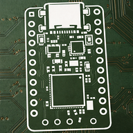
I completely finished all the lines and vias, Everything went well with no errors when drcing and I now think I could do the flight controller,
here is a photo of my completed devboard:

kjnox206
added to the journal ago
Super close to finishing routing
Almost done routing my pcb but getting very stuck because of the lines and this will probably be the last time doing this project, so sorry but this guide did not make as much sense as the hackpad one did.
Heres a photo of where Im currently at:

kjnox206
added to the journal ago
I routed some of the pcb
I started doing the routing of the pcb, this is getting annoying because you have to think of all the connections and trying to make it so that everything can go to where it should go.
Here's a photo of where I am at currently:

kjnox206
added to the journal ago
I followed the guide until I got stuck
I got stuck at this point: Then, hold the route tracks button, and go over to the symbol with 2 traces on it, or just tap 6. Then, go over to your USB-C, and tap on one of the D+/D- pins to start the trace, and route it down to your resistors. If the traces won't go into your resistors pads, that means that your resistors aren't evenly positioned, you can just the relative positioning tool to do this.
And then you can just route the resistors nets into the RP2040 nets (Make sure they're centered so the traces are the same length, you could technically do this as a differential pair if you change your schematic slightly, but it's fine if you just position properly):

this is my problem:

zoomed in:

kjnox206
added to the journal ago
I followed the custom devboard guide
I followed the custom devboard guide until this point:
"And then, we're going to change the flash memory to what the Pi Pico uses and has a slightly smaller package, which is the W25Q16JVZPIQ TR and uses the PackageSON:WinbondUSON-8-1EP3x2mmP0.5mm_EP0.2x1.6mm footprint, which isn't the exact footprint, but should work fine:"
which made be confused because there isnt a W25Q16JVZPIQ TR when I looked it up in the footprints:

this is what I have so far:


kjnox206
started Knox's Custom devboard rp2040 ago
1/12/2026 - I followed the custom devboard guide
I followed the custom devboard guide until this point:
"And then, we're going to change the flash memory to what the Pi Pico uses and has a slightly smaller package, which is the W25Q16JVZPIQ TR and uses the PackageSON:WinbondUSON-8-1EP3x2mmP0.5mm_EP0.2x1.6mm footprint, which isn't the exact footprint, but should work fine:"
which made be confused because there isnt a W25Q16JVZPIQ TR when I looked it up in the footprints:
this is what I have so far:
1/13/2026 6 PM - I followed the guide until I got stuck
I got stuck at this point: Then, hold the route tracks button, and go over to the symbol with 2 traces on it, or just tap 6. Then, go over to your USB-C, and tap on one of the D+/D- pins to start the trace, and route it down to your resistors. If the traces won't go into your resistors pads, that means that your resistors aren't evenly positioned, you can just the relative positioning tool to do this.
And then you can just route the resistors nets into the RP2040 nets (Make sure they're centered so the traces are the same length, you could technically do this as a differential pair if you change your schematic slightly, but it's fine if you just position properly):
this is my problem:
zoomed in:
1/13/2026 10 PM - I routed some of the pcb
I started doing the routing of the pcb, this is getting annoying because you have to think of all the connections and trying to make it so that everything can go to where it should go.
Here's a photo of where I am at currently:
1/17/2026 - Super close to finishing routing
Almost done routing my pcb but getting very stuck because of the lines and this will probably be the last time doing this project, so sorry but this guide did not make as much sense as the hackpad one did.
Heres a photo of where Im currently at:
1/18/2026 - Well I guess I just need some time to figure it out.
I completely finished all the lines and vias, Everything went well with no errors when drcing and I now think I could do the flight controller,
here is a photo of my completed devboard: