How to Order from JLCPCB
First time ordering from JLCPCB, or PCBs in general? Or do you just need a refresher on ordering PCBs? Either way, you’re in the right place!
1. Getting Gerbers
PCB fabs take files called Gerbers. These are essentially outputted directions from whatever software you used (EasyEDA, KiCAD, etc) that contains information about the copper on the board, any silkscreen designs you have, and where to drill holes.
Getting Gerbers is easy. They are usually under some sort of export or output section of your software.
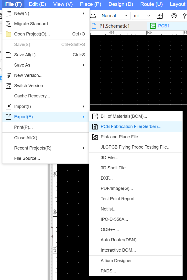
For EasyEDA, simply go to your PCB view (not the schematic view) and click
File>Export>PCB Fabrication File(Gerber).
It will prompt you to check DRC which you should ALWAYS do
If you are doing PCBA (A PCB board with the parts assembled at the factory), you will also need the Bill of Materials(BOM), and a Pick and Place File. You can get them by doing:
File>Export>Bill of Materials(BOM)
File>Export>Pick and Place File
2. Uploading to JLCPCB
Once you have your Gerbers, make sure they are zipped up so you can upload the folder all in one piece.
What the Heck are These Settings?
PCB fabs have a lot of settings for board manufacturing, and JLCPCB is no exception. Here’s a rundown on what each section means:
Base Options
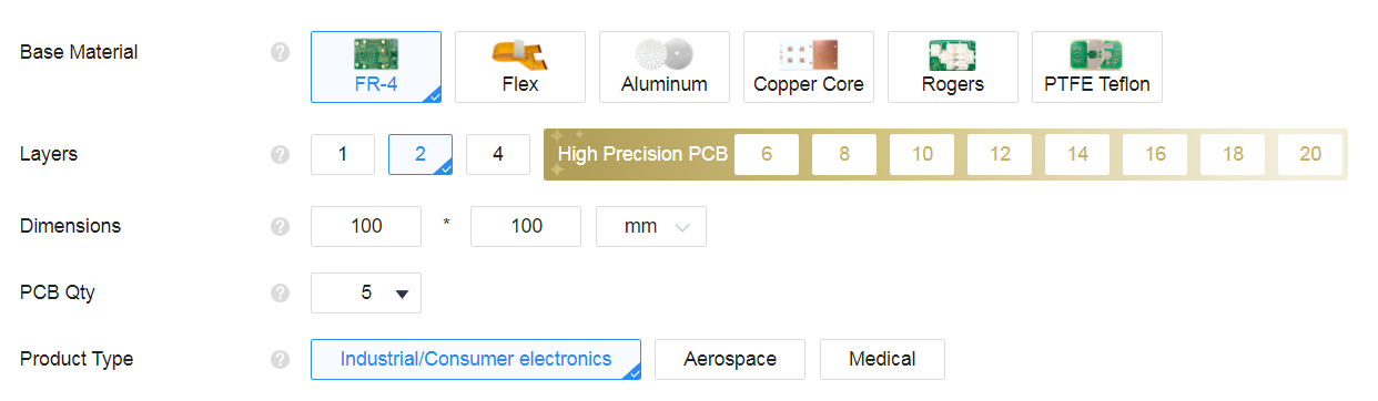
Base options (These are all the default options so you likely don’t need to change anything)
- Base Material: Use FR-4.
- Layers: 2 is the most common.
- Dimensions: Auto-filled from your Gerbers. > Note: The PCB is a lot cheaper when below 100mmx100mm so if you are close to that number, maybe try redesigning to be under
- PCB QTY: Choose 5 (minimum allowed).
- Product Type: Keep as Industrial/Consumer Electronics.
PCB Specifications
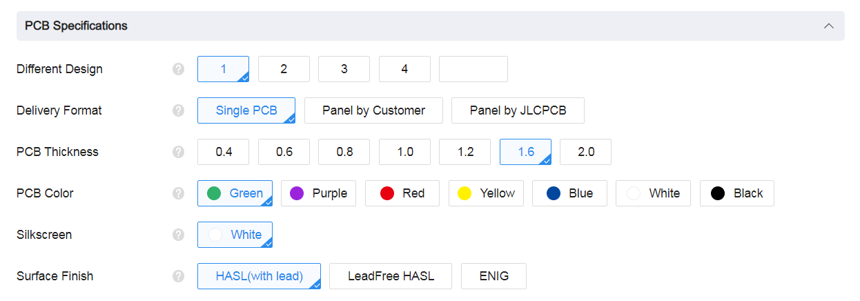
PCB specs
- Different Design: Auto-calculated.
- Delivery Format: Use
Single PCB. - PCB Thickness: Keep at 1.6mm.
- PCB Color: Green is cheapest.
- Surface Finish: Lead-free HASL or ENIG.
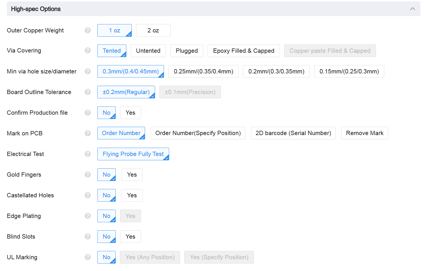
High-spec Options
High-spec options
Try and always keep the high-spec options on the default. Changing them is quite expensive.
3. PCB Assembly
Choose one of two assembly options for your PCB. Assembly by JLCPCB is the quickest and easiest.
Assembly by JLCPCB
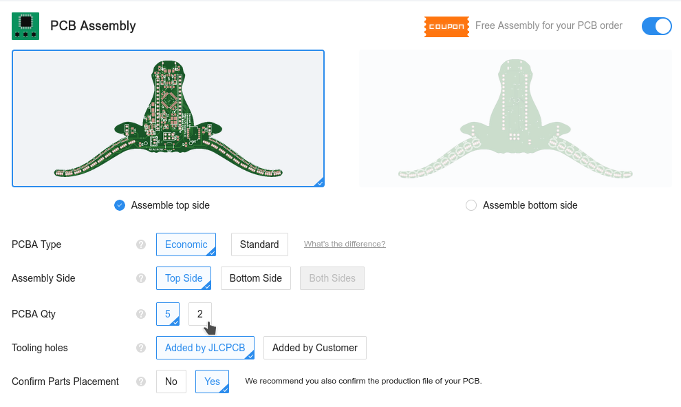
Assembly options
- PCBA Type: Choose Economic.
- PCBA Qty: 2 is enough to save cost.
- Confirm Parts Placement: Optional, useful check.
Then upload your bom.csv and positions.csv (KiCad) or BOM_PCB.csv and PickAndPlace.csv (EasyEDA).
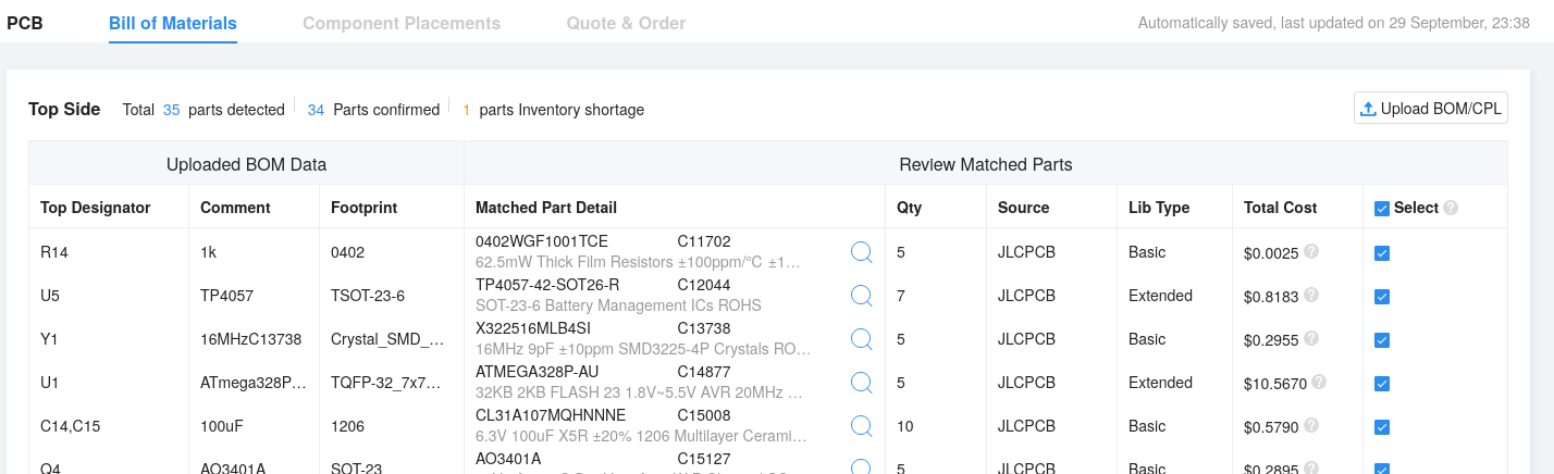
BOM Upload
If parts like the NFC antenna are unselected, click “Do Not Place”.
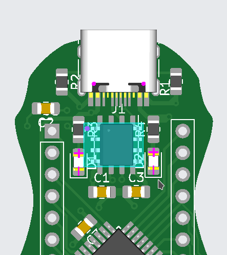
Orientation
Note: Resistors/most capacitors are bidirectional, but diodes, LEDs, and ICs are not.
Assemble Yourself with a Stencil
Don’t want to pay extra for assembly? DIY is a great, hands-on learning option, but it’s for advanced hackers only.
You’ll need a soldering iron, solder paste, and a heat gun or reflow tool.
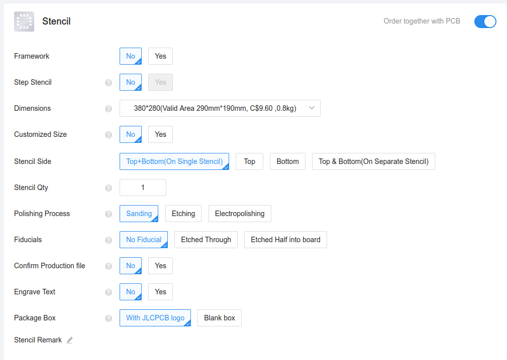
Stencil
Learn more: YouTube guide or PCB Elec guide
4. Cart
Click checkout and fill out your information.
To avoid excess shipping fees or customs, check out the Shipping Tips doc!
The TLDR is that you should select Global Standard Direct for your shipping only if you can!
Then choose “Pay after Review” or “Pay Directly”, and click Submit Order.
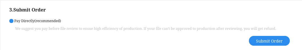
Submit order
Once asked for payment info, you can just close the tab.
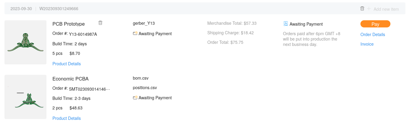
5. PCB Review
Go to My Orders and take a screenshot like below: