Mini Midi Magic

Welcome to mini midi magic! This is a kickstart guide to help you get started with designing and building your own midi device and point you towards practical resources to help you make something cool for the world to see (and hear)!
Table of contents
- Basic rules
- What’s in the kit
- Getting started
- Designing Schematic
- Designing PCB
- Making a case
- Writing the firmware (Circuitpython)
- Submitting!
There will be another guide for assembly later.
Basic Rules
- You must be a high-schooler or younger.
- Your project must be an original submission.
- You must create and submit a journal of all the steps that you took to design your project, with time spent on each section.
- Hackatime is not required to submit your project.
- You are only allowed to make one submission.
- You must include a readme, with images and renders of your project. ## What’s in the kit
- Orpheus Pico
- TFT LCD
- Rotary Encoders
- Switches and buttons
- Slide potentiometer
- PCM5100 I2S DAC Breakout
- Some M3 Mounting material
- Screws
- Threaded inserts
- Diodes (for your switch matrix)
- Resistors and capacitors (specify in the submission form!) ## Getting started This guide covers the essential steps needed to make a simple mini device, and teaches you to implement the folowing things in both circuit design and code.
- Switches and keys (in matrix)
- Rotary encoders
- TFT LCD
- PCM5100 IIS DAC
The schematic will teach you how to interface all of these features into your single microcontroller while being smart with your pin usage!
Designing a schematic
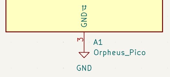
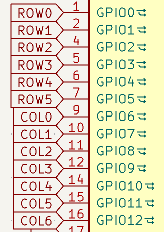
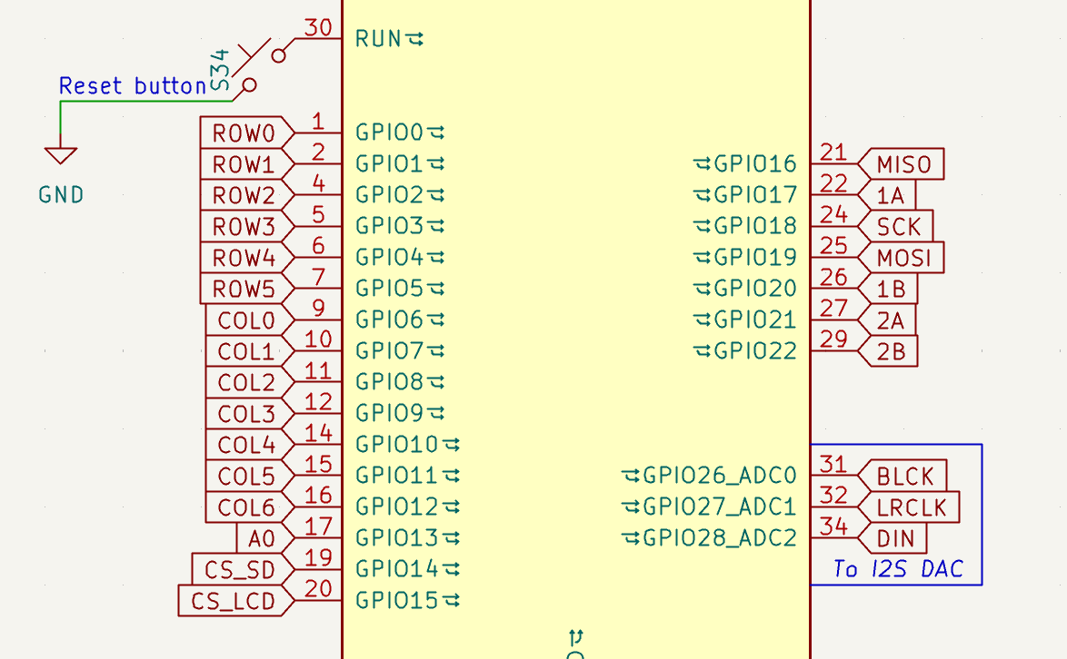
The schematic for this project must include the orpheus pico. Since the orpheus pico is pin compatible with the normal pico, we can just use the same symbol as the regular raspberry pi pico which comes preinstalled with modern kicad.
Make sure to connect your GND and AGND to the ground symbol and connect your 3v3 to a +3v3 symbol. This will make it easier when you power certain devices later.
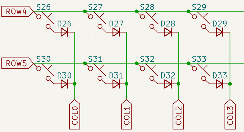
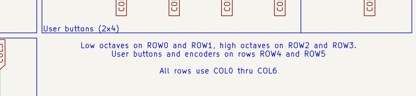
Switch matrix
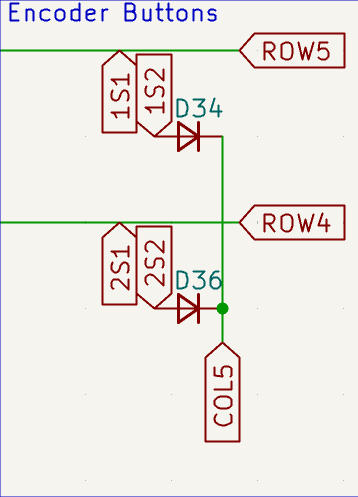
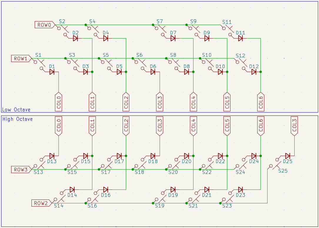
The switch matrix is used to reduce the number of GPIO pins necessary for each key. It is generally preferred over using each key individually, as you can use a larger number of keys in the same number of pins. A 6x6=36 matrix can be used instead of 36 individual keys to reduce the number of pins needed from 36 down to 6+6=12.
In a matrix, the keys are arranged in rows and columns and each key press is detected by scanning the rows and columns to find the active key. However, this alone causes issues when multiple keys are pressed simultaneously. Thus, we use diodes between the keys to prevent ghosting and make sure that each key is detected properly. For this, we first lay out all our switch symbols in a table. Each key should be positioned in a single row and column.
No two keys should share the same row and column
. The diode we use is the 1N4148, which is a cheap and convenient diode and popular for this application.
When connecting, make sure all the diode directions are the same. Either use column -> row (COL2ROW) or use row -> column (ROW2COL) throughout all the switches.
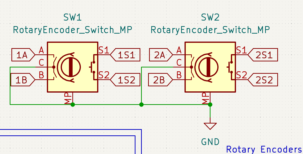
Rotary Encoders
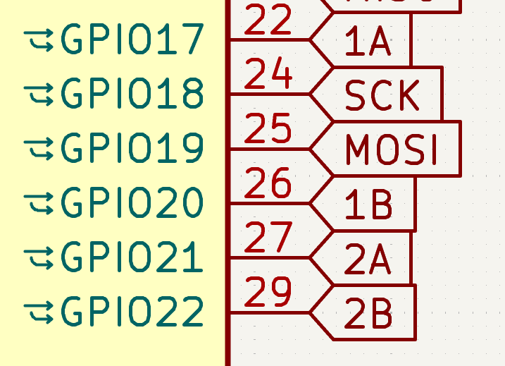
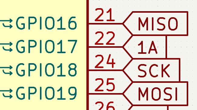
We will be using EC11 rotary encoders. Add the symbol RotaryEncoder_Switch_MP. The switch means that it is clickable, and the MP stands for mounting points, which are the pads connected to the base of the mounting pins of the encoder. These pins are used to physically hold the encoder in place. Connect the central C pin and the MP to your ground. SW1 and SW2 connect to your regular switch matrix, following the same COL2ROW or ROW2COL convention as the other switches, with the same diode. The A and B pins connect to your microcontroller’s GPIO pins, and are used to measure the signals. We will not go too deep into this because most firmware tools have libraries ready for encoders.
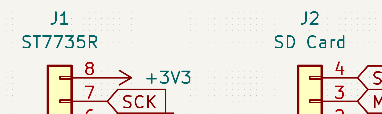
TFT LCD
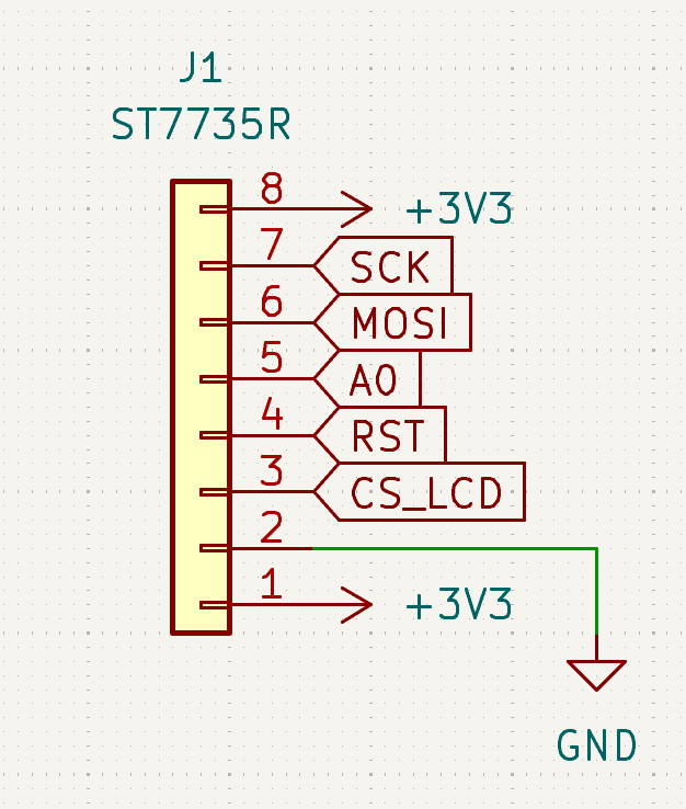
For this project, we will be using the ST7735R LCD, which is a great LCD with a nice resolution, and it’s broken out via SPI. The SPI interface makes it really easy for us to add this display while keeping complexity low. The one we will be using has the following pinout (from top to bottom) -
LCD
,
SCK
,
SDA
,
A0
,
RESET
,
CS
,
GND
and
VCC
. For this, we will simply add a 1x8 connector to the schematic, and label it with the text tool.
- The LCD pin provides the LCD Backlight power, we can use this to control brightness and the backlight itself. If you are not changing the backlight, connect this to 3v3 or use an unused GPIO (you can use PWM later to control the brightness).
- The SCK (Serial Clock) pin provides a SPI Clock signal to the LCD. Just connect this to an SPI Clock pin on the microcontroller.
- The SDA (Serial Data) pin provides the data signal to the LCD. Connect this to an SPI MOSI (TX) pin on the microcontroller.
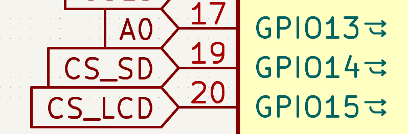
- The A0 (Data/Command) pin is used to switch between data and command modes. Your display library usually handles this field, so just tie it to any open GPIO.
- The RESET pin is used to soft reset the LCD, simply connect this to any GPIO.
- The CS (Chip Select) pin is used to select the LCD for communication on an SPI bus with multiple devices. While you can directly connect this to 3v3/GND (depending on active low or active high modes), it’s generally better to connect it to a GPIO pin and control it in software.
- The GND pin and the VCC pin connect to your board’s ground and +3v3 power symbols respectively. In the given example, the SPI bus is also shared with the SD Card on the LCD, so the CS pins must be different so that the bus can be the same.
PCM5100 IIS DAC
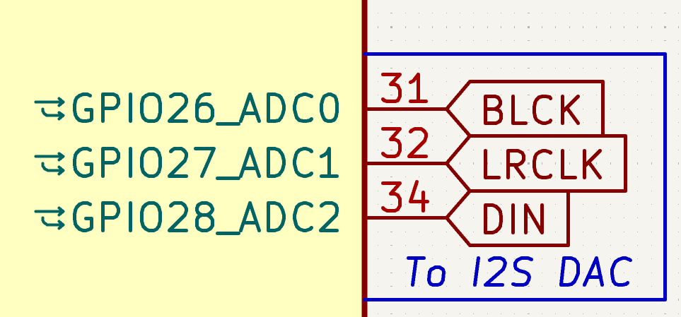
For audio output, we will be using the PCM5100 IIS DAC. This DAC provides high-quality audio output and is controlled via I2S (Inter-integrated Circuit Sound), an easy digital protocol to control audio devices via microcontrollers. In this example, I’ll be using the raw pins rather than a breakout board, as this varies between applications. The 3 main pins we need to deal with are
BCK
,
LRCK
, and
DATA
.
- The
BCK
pin is the Bit Clock pin, which provides a clock for the DAC to use (Similar to SCK).
- The
LRCK
pin is the Word Select pin, which indicates the start of a new word (instruction).
- The
DATA
pin is the Serial Data pin, which handles the main sound data between the microcontroller and the DAC.
- The
GND
pin and
VCC
pin can be connected as in the LCD example, just connect the
GND
to your schematic’s ground symbol and the
VCC
to +3v3.
A little bit more on the schematic
Your schematic is mostly ready to go around this point, but you should take a few steps to make it look cleaner and easier to read!
- Use bounding boxes around certain sections of the schematic to group certain areas. Visually seperate if a set of buttons is used differently from another in the schematic too!
- Use labels instead of connecting far components! Sometimes, labels might become easier to read when your schematic has a lot of components, and they are all placed distant from the main microcontroller.
- Add text to explain certain confusing sections. Maybe you have a few different matrixes with different purposes? Label them with the text tool to let people know what those sections mean.
- Make sure to label your jumpers. The LCD and the DAC breakout jumpers might still have the
CONNlabel on them, double click it to rewrite it as your screen or breakout. You can also leave it as it is and add some text to clarify headers next to it.
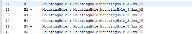
- Also add some unconnected mounting hole footprints! These will be used later to make holes in your PCB that will screw into the case!
Footprint Assignment
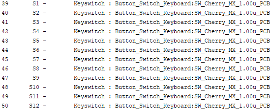
The next step is to assign footprints. With the footprint assignment tool open, you need to click on each unassigned component and select a footprint from the panel on the right. You need to use the searchbar to get meaningful results. If you are confused, you can right click the footprint after selecting it to view the footprint in the footprint in the editor. Use the measure tool to compare the dimensions with the standards mentioned in the datasheet. Some of the footprints you may need for this project include:
PinHeader 2.54mmfor the jumpers (select the correct size).Raspberry Pi Pico THTfor the main microcontroller.MX_PCB_1.00ufor any MX (keyboard) switches.RotaryEncoder_EC11-Switch_Vertical_H20mm-MountingHolesfor the rotary encoders.MountingHole_x.xmm_Mxfor mounting holes. Since I am using M3 screws, this will beMountingHole_3.2mm_M3. Some of these names might be different based on your kicad installation and the libraries you have installed with it. Don’t be afraid to ask if you can’t find your desired footprints!


Designing a PCB
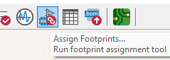
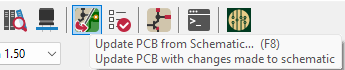
Now that we are done with the schematic, we can apply all changes to the footprint assignment and move on with the PCB. Start by pressing the Convert schematic to PCB button (shown below). This should take your footprints and add them to your PCB. If there are any errors, cross check the footprints associated with them and make sure they even exist!
Component Placement
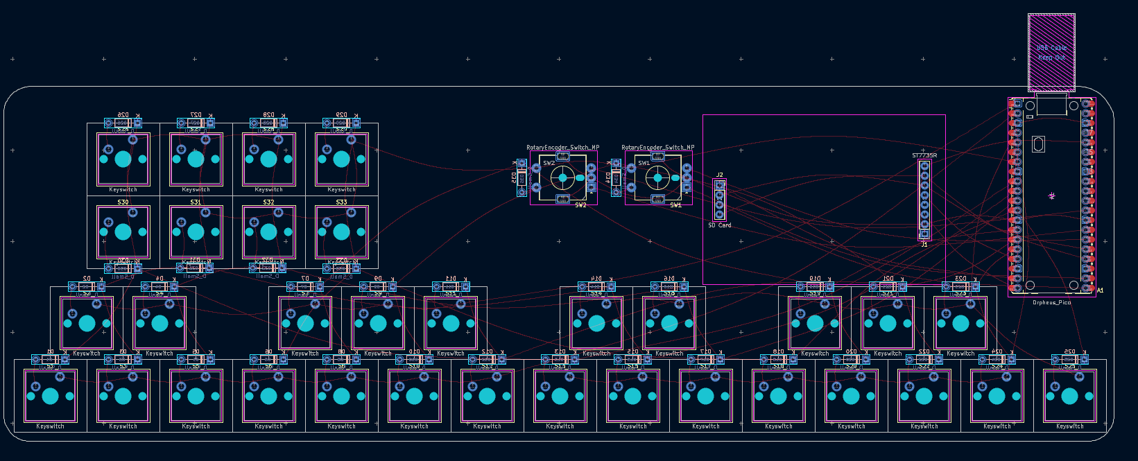
To get started, place your components around the PCB layout as your need. You might want to use the grid tool to change the grid sizes to make it easier to place certain footprints. Eg. You should change the grid size to a submultiple of 19.05mm x 19.05mm when placing MX switches, because that is their clearance in an actual keyboard/keypad! You can also use the Grid origin tool to set a different origin than your actual board. Once all your components are placed, you should create an edge cut. Select the Edge.Cuts layer and using the rectangle/polygon tool, sketch out the PCB cutout. If you want curves, you can use the arc or the curve tool.
Here is my design!
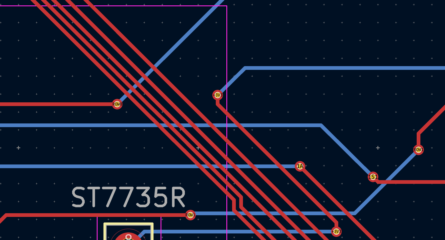
Routing your traces
While a lot of people might start with an autorouter, it isn’t always perfect. Instead, it is best to manually check every trace and every route. Keep traces as short as possible and straight to the point. Don’t be afraid to use vias to switch your trace between layers, because you won’t be paying extra for them! If your traces are too jumbled, you might want to consider erasing that certain area to reroute them better. A personal tip is to have long horizontal traces be on the opposite layer as long vertical traces, as you will not need to use vias as often and your board will be overall cleaner and easier to debug.
Silkscreen
The silkscreen layer is used to add cosmetic effects to your PCB’s top layers. You can use the text tool while either F.Silkscreen or B.Silkscreen are selected to write text. The polygon tool is also adapted to create filled shapes, and you can even insert logos using kicad’s built-in image conversion tool! This includes anything from decals to cool graphics. Logos, labels and text is very common, so make sure to use the silkscreen to it’s fullest potential and create something cool!
Making a case
[gonna let someone else take this one]
Writing the firmware
The firmware for the board is the code that dictates the microcontroller into handling all the inputs and outputs. For this guide, we will be using circuitpython, due to it’s dedicated support with so many of the parts we will be using! To get started with circuitpython, head to their downloads to get the .uf2 file for the pico! If you will be prototyping at home, use whichever pico you have right now. Once you receive your kit, you can use the Orpheus Pico download. Here is a list of things we will be designing in this example!
- Switch/key matrix
- Rotary Encoders
- TFT LCD (ST7735R)
- I2S DAC (PCM5100)
- MIDI over USB
Switch/key matrix
For the matrix we will be using circuitpython’s built-in keypad library! This library provides direct support for handling key matrices and makes it easy to read the state of each key as an event, which you can iterate to fetch data.
Start by creating a KeyMatrix object using the library
import board
import keypad
import digitalio
rows = [board.GP0, board.GP1, .....]
cols = [board.GP0, board.GP1, .....] # Make sure to use your actual GPIO pin numbers!matrix = keypad.KeyMatrix(rows, cols, columns_to_anodes=True/False) # True in the case of COL2ROW, else use False if using ROW2COL
This creates a matrix object for our key matrix. Now we need to setup the method to read the events of the matrix.
while True:
    event = matrix.events.get()
    if event:
        print(event.key_number, event.pressed)
This code will print the key number and its pressed state when a key is pressed/released. You can use the event.pressed boolean to identify if it was pressed (True) or released (False). The key_number corresponds to your matrix position. You can combine this with any functions to modify the LCD, send midi inputs, change settings and really anything at all!
Rotary Encoders
For rotary encoders, we will be using the rotaryio library, which provides a simple interface to read rotary encoders. The library handles the A and B pins of the encoder and provides a value that can be used to determine the rotation direction and amount.
First, we must configure the encoders using the library.
import rotaryio
encoder = rotaryio.IncrementalEncoder(board.GP0, board.GP1) # Your actual A and B encoder pinsenc_pos = None # Set position variable outside loopwhile True:
    pos = encoder.position
    if pos != enc_pos:
        print("Encoder position:", pos)
        enc_pos = pos
This code will update and print the changing encoder positions. You can also define any divisor if you wish, to change the increments needed to modify position. 4 by default works great!
TFT LCD (ST7735R)
For the TFT LCD, we will be using the displayio library, which provides a simple interface to work with displays. The library supports various display drivers, including the ST7735R.
First, we must configure the display using the library.
from adafruit_st7735r import ST7735R
import displayio
import busio
from fourwire import FourWire
displayio.release_displays()  # clear any display from previous runsdisplay_bus = FourWire(
    bus=busio.SPI(clock=board.GPxx, MOSI=board.GPxx),
    command=board.GPxx,
    chip_select=board.GPxx,
    reset=board.GPxx
)
display = ST7735R(display_bus, width=128, height=160, rotation=xx)
The rotation depends on your orientation and must be 0, 90, 180 or 270.
Let us try setting the entire display to a solid colour.
splash = displayio.Group()
display.root_group = splash
color_bitmap = displayio.Bitmap(160, 128, 1)
color_palette = displayio.Palette(1)
color_palette[0] = 0x00FF00
This creates a bitmap the size of the screen, creates a pallete with one colour and tehn adds the colour to the palette. In this case, 0x00FF00 is the colour for green. If you have some basic knowledge of hex codes, you can change this to any colour you want.
bg_sprite = displayio.TileGrid(color_bitmap, pixel_shader=color_palette, x=0, y=0)
splash.append(bg_sprite)
You can also add text to the display!
import terminalio
from adafruit_display_text import label
To add a label, we create a text group for the label and then append our text, font and colour to it. Lastly, we append the label to our original splash group to update the display.
text_group = displayio.Group()
text = "wsg hackclub"text_area = label.Label(font=terminalio.FONT, text=text, color=0xFFFFFF) # White texttext_group.append(text_area)
splash.append(text_group)
This now appends our text to the screen! You can change the size and position by modifying the x and y parameters of the text_group. You can change the colour by changing the color parameter of the label.
You can use the various features provided in displayio, vectorio, and the various other libraries to create custom UIs, animations, stats, starting screens, and so much more! This is just scratching the surface on how to get your LCD started and some of the cool stuff you can do on it!
I2S DAC (PCM5100)
The I2S DAC is connected to our microcontroller by 3 main wires we need to worry about (BCK, LRCK, DATA). We will be using the audiobusio library to implement this feature. First, we must initialize the DAC on the I2S bus.
import audiobusio
dac = audiobusio.I2SOut(bit_clock=board.GP0, word_select=board.GP1, data=board.GP2)
You can generate some sounds on the go like sine waves, but anything more advanced should ideally be a .wav on your filesystem (good thing the orpheus pico has 8 whole megabytes!), and you can play it easily by loading it onto the device.
import audiocore
wavf = open("soundthing.wav", "rb")
wav = audiocore.WaveFile(wavf)
dac.play(wav)
while dac.playing:
    pass #because if the code ends then the sound ends
You can use this to hold many different noises and generate sound effects on the go! Just note that there may be some latency so good luck using this for actuial covers or performances.
MIDI over USB
So now that your inputs are working, it’s time we start getting your device to send MIDI outputs!
We will be using the usb_midi library to send MIDI messages to a host computer, and the adafruit_midi library to encode our messages. Do note, the adafruit_midi library is not included by default, so you will need to install it using the CircuitPython bundle.
To get started, import both the libraries and start a midi connection.
import usb_midi
import adafruit_midi
from adafruit_midi.note_off import NoteOff
from adafruit_midi.note_on import NoteOn
from adafruit_midi.pitch_bend import PitchBend
midi = adafruit_midi.MIDI(
    midi_in=usb_midi.ports[0], in_channel=0, midi_out=usb_midi.ports[1], out_channel=0)
midi.send(NoteOn(60, 127))
midi.send(NoteOn(64, 127))
midi.send(NoteOn(67, 127))
time.sleep(1)
midi.send(NoteOff(67, 0))
midi.send(NoteOff(64, 0))
midi.send(NoteOff(60, 0))
# C major chordmidi.send(NoteOn(60,127))
midi.send(PitchBend(0, 16383)) #woo pitch bend
The adafruit_midi library has a lot more information you can use to implement features like MIDI CC messages and more advanced features. Check out their docs here:
You can also find additional information on the other docs in the firmware guide here:
Submitting
Before submitting, make sure you have completed the following steps:
- Have a complete schematic, PCB design and a production folder with the gerber files.
- A code folder with any firmware files copied from/to your circuitpython device.
- A case design, with a step model including the PCB and any other components.
- A bill of materials (BOM) listing all components used in the project.
- You need to mention all the components regardless of whether or not they will be included in the kit.
- If you use any components that you wish to purchase with your grant, those must be marked as such in the BOM.
- You must also add the total cost of these extra components while filling the submission form.
- A complete journal describing your process that includes the hour count of each session on each section of the project.
- A readme file with images and renders of your project, including a description of the project and its features. Once all of these requirements are fulfilled, fill out the submission form here.