Wireless split
Made by @koeg
Hii! Do you not want to get carpal tunnel? Or just think that split keyboard are cool? Then you are in the right place!
In this guide you will be learning how to make a wireless split keyboard
This guide is meant to be an extension to the hackpad guide, so if you are a total beginner to keyboards/electronics, read that first, and then come back here :)
In this tutorial we are going to use the same form factor board as in the hackpad tutorial, but with different internals. Instead of a rp2040 it has a nrf52840 chip inside, which has wireless capabilities.
If you want to dive a little bit deeper before starting, Joe Scotto has some good videos on how keyboard work and on how kicad works
This guide is made by @koeg on slack, so if you have any questions about this ask in #blueprint-support and tag me. Thr source files of this project can be found in this repo.
Installing Libraries
After you created the kicad project, we need to install some libraries. We will be installing the same OPL libraries as in the hackpad tutorial, here is the link for that section.
Unlike in the hackpad tutorial, where we used the official seeed footprints, this time we need to install a custom footprint based on the official ones. Because the battery charging pins are on the bottom of the board, which we will be using to charge the battery, they are not accessible if we use the official footprints.
You can download it from github, move it into your KiCad project folder, and add it like the OPL library.
We also need to download the library for the switches, we will be using marbastlib, you can find the installation instructions in the repo
Also install panelization.pretty for mousebites
Schematic
Now we can start creating our schematic.
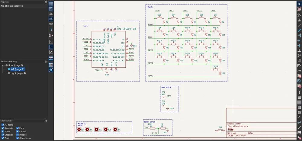
Sheets
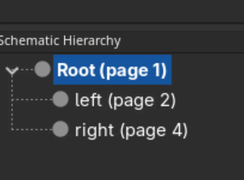
Because we are creating a split, we essentially want to have the same circuitry for both sides, but not the same layout. We can achieve this by using hierarchical sheets. This way the circuitry we make will be duplicated.
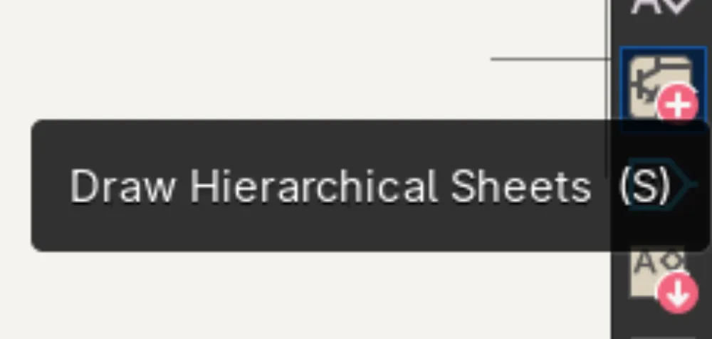
To create a hierarchical sheet, click on this icon on the right sidebar or press S
Now draw a rectangle and left-click; a popup should appear:
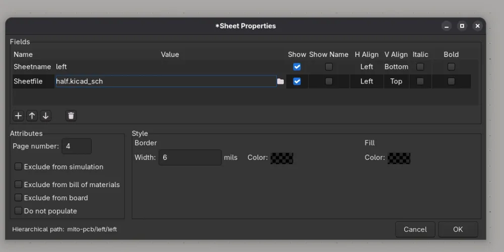
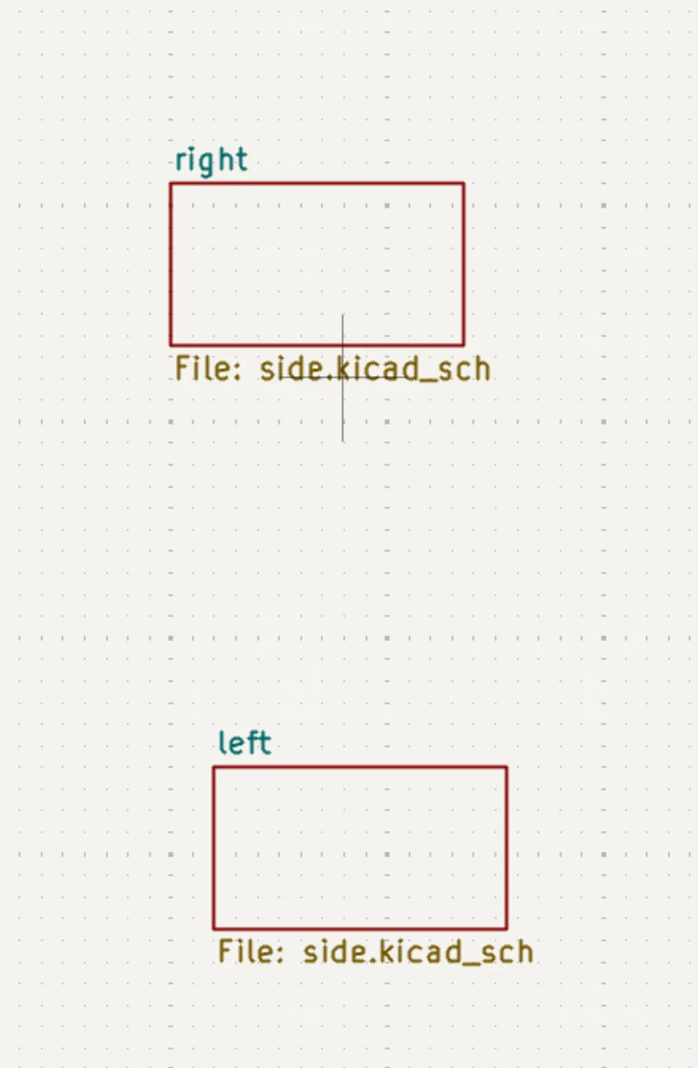
Change the Sheetname to left, and the Sheetfile to side.kicad_sch, and click ok
Now create another sheet, set Sheetfile to side.kicad_sch, but the Sheetname to right.
Your root sheet should look something like this:
And your left sidebar something like this:
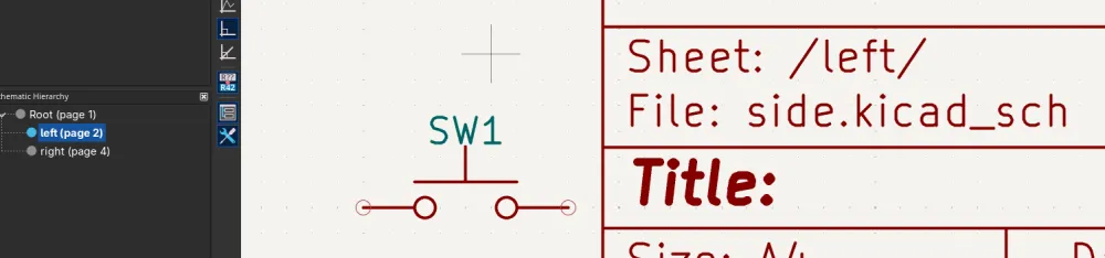
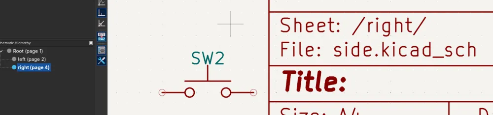
You can now double-click on one of the sheet rectangles in the root sheet or in the left sidebar. You can now place down a switch, for example, and navigate to the other sub/child sheet. You will notice that the switch that you placed down in the other sub-sheet is also in this sub-sheet.
Circuitry
Now finally we can start to design our keyboard!!!
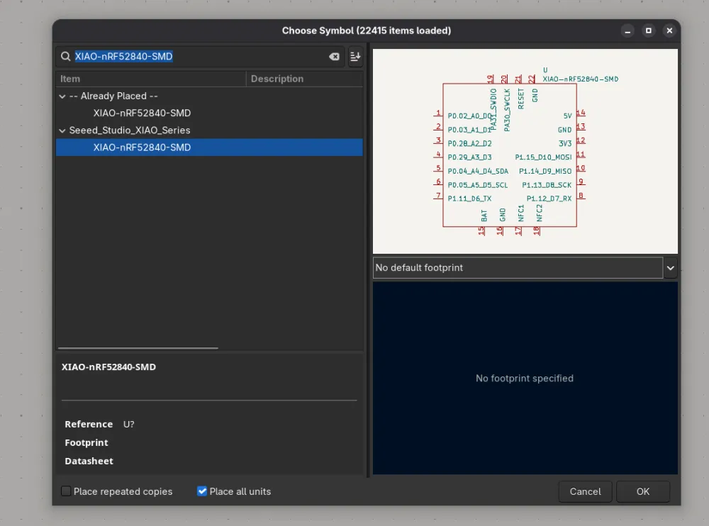
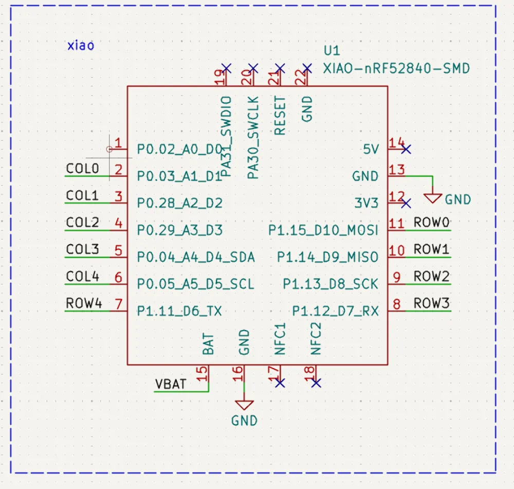
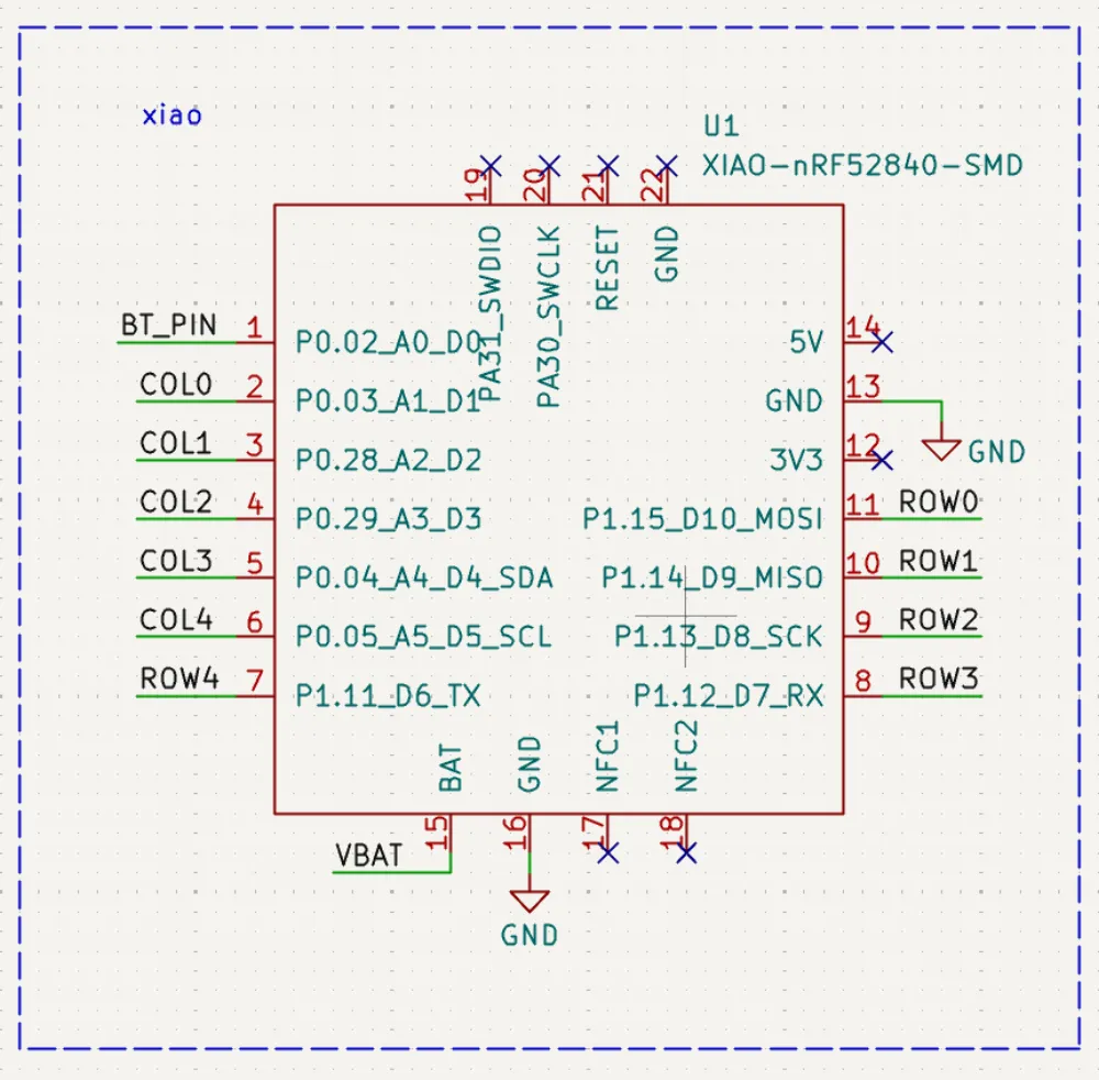
Add the XIAO-nRF52840-SMD symbol:
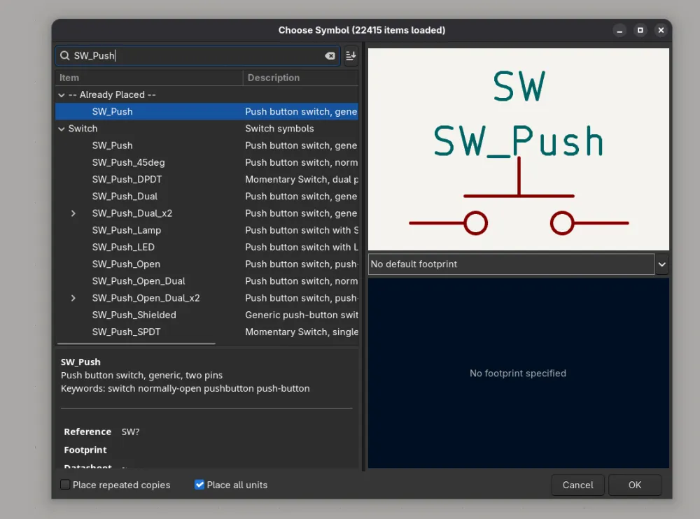
a switch SW_Push:
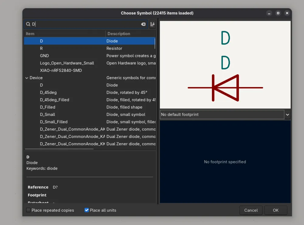
and a diode D (you will see later why we need this):
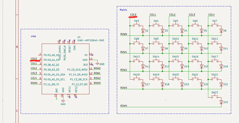
Keyboard Matrix
You may be wondering, why did we need to place down a diode???? You may also notice that the Xiao doesn't have enough pins for a full half of a split keyboard. In comes the humble keyboard matrix; with it we only have to connect one pin per column and one pin per row, drastically reducing the number of pins needed for a keyboard.
The matrix works by giving power to each column one at a time and checking which keys are pressed down in that row. The matrix will represent our final keyboard layout on our PCB, in this example if we have 4 rows and 5 columns, and one lonely thumb button in the 5th column and the 5th row, in our matrix in the schematic. We will have the same layout of switches on our PCB. We need diodes to prevent ghosting, whereby pressing down one key, the keyboard detects more than one keypress. If you want you can read into keyboard matrixes here.
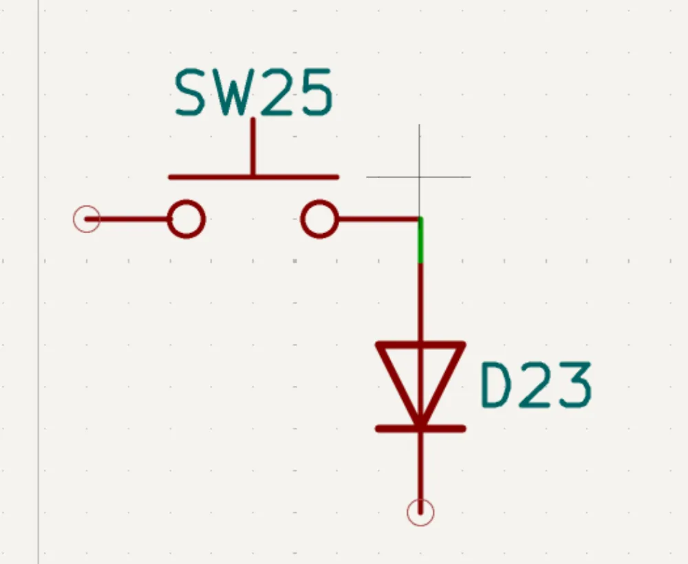
For now all you need to know is that every key has its own diode; this is like one unit:
You can now make a matrix out of these units; you have to connect the switches to the columns and the diodes to the rows. In this example, in one row I only have one button, which is for my thumb:
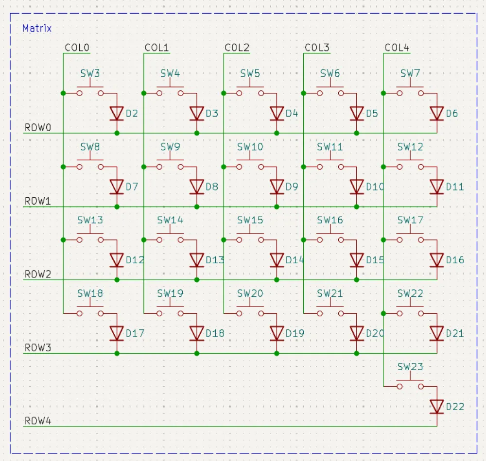
You may notice that there are labels, like COL0, COL1, etc., and ROW0 and ROW1. These are labels. You can place these using the L shortcut or from the right sidebar. We can use labels to clean up our schematic. Instead of routing from our Xiao to the column, we just place a label with the same name at the column and one at the Xiao's pin:
Battery
Adding a battery is really easy because the Xiao already has battery management built in. We need to add two pads where the battery can be connected to the PCB. In this case I used two test points, one for the negative side of the battery (aka ground) and one for the live side (aka vbat):
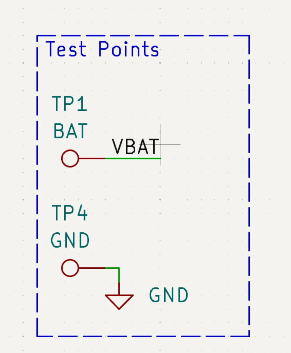
And then connect the pin VBAT to the BAT pin of the xiao
Sensing the battery voltage
This is an optional feature that lets you see from your computer how much juice is left in your keyboards.
We can achieve this by using a voltage divider, basically two resistors that divide the battery voltage by an amount, so we can measure it with our Xiao. It looks like this. Make sure to use these values for the resistors:
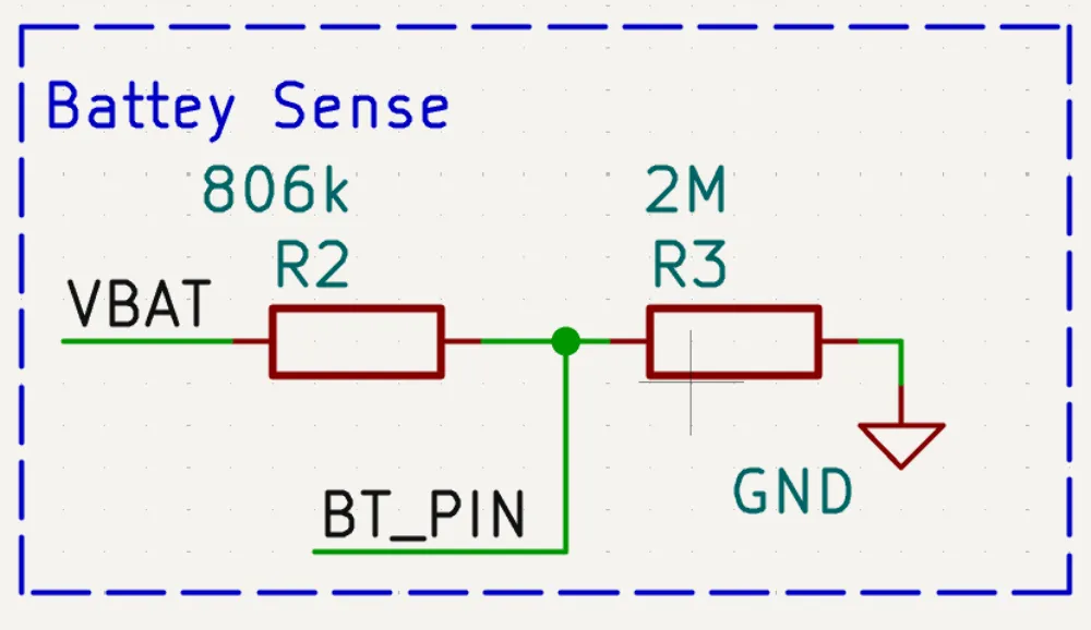
And then add the corresponding label (BT_PIN in our case) to the Xiao; make sure that it is an analog pin (has A* at the end):
Mounting points
In one of the hierarchical sheets, add 4-6 mounting points. I recommend you use M2-M3 screws.
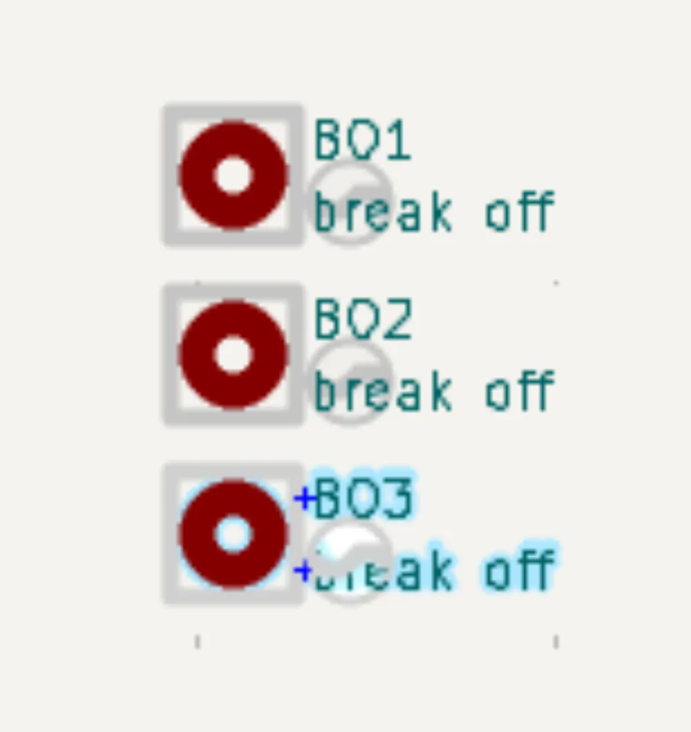
Mousebites
You should add three mounting points to the root sheet; we will assign mousebite footprints to these later on
Footprints
You're done with your schematic!!!
Here is how mine looks:
Now it's time to assign some footprints! First, open the footprint assigner tool.
For the Xiao, assign the custom footprint that you downloaded earlier; its name should be modified-XIAO-nRF52840-SMD
For the buttons I used chalk hotswap sockets from marbastlib, but you can use any other keyswitch.
For the diodes I used 1N5819 which are SMD, so it's a bit harder to solder, but I recommend them if you want a compact design. If you go for THT diodes, don't place them next to the switches but rather somewhere else on the PCB. The footprint for this is Diode_SMD:D_SOD-123
For the resistors, I recommend Resistor_SMD:R_0805_2012Metric, but you can use any other package.
For the mousebites/breakoffs, assign the panelization:mouse-bite-5mm-slot footprints from the library that we downloaded earlier
For the testpoints/battery pads, I used TestPoint:TestPoint_Pad_D2.0mm, but you can use larger.
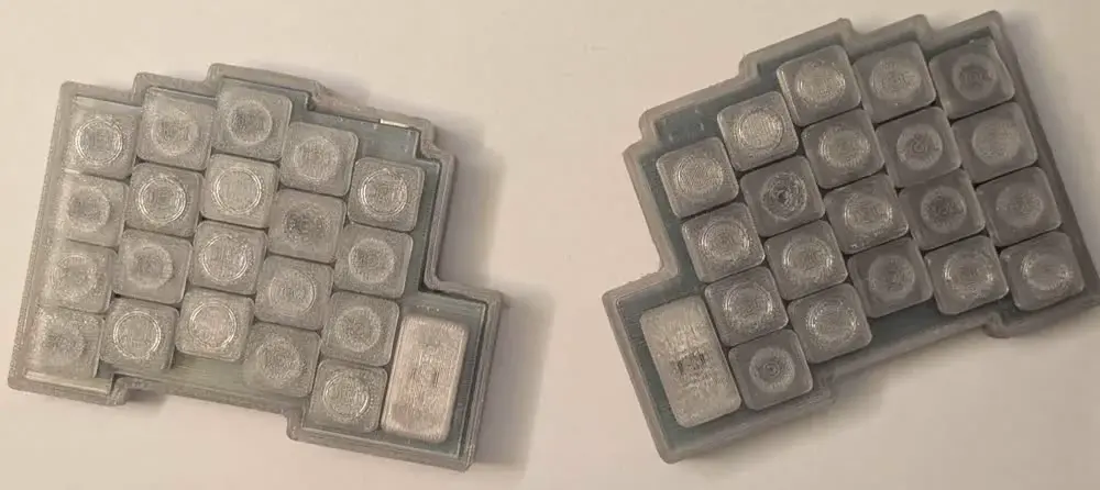
PCB
This part is basically the same as hackpad, so layout, then routing, except for the mousebites. So in this section I will give some tips for laying out a split keyboard
Here is my final pcb:
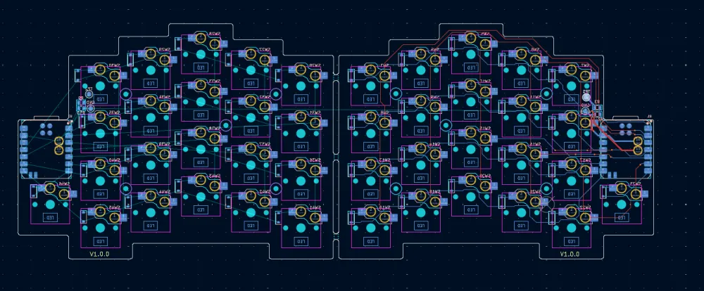
If the two halves are symmetrical
then you should make the edge.cuts for one half, select all the edge.cuts, right click, and flip horizontal, and now you have two symmetrical edge.cuts
Mousebites layout
You should find two flat sides of your two PCBs, place the mousebites there, and edit the edge cuts so it matches the mousebites footprint template:
Firmware
You will have to use the ZMK firmware, ZMK has excellent documentation and tutorials, and it explains it better then I could. It has a learning curve, but there is no getting around that