Let's Design an RP2040 Devboard!
Made by @Kai Pereira
Today, we're going to be designing our own dev board, using one of the most popular and beginner friendly SoC's, the RP2040. This guide doesn't serve as just a tutorial, but also as an opportunity to learn what everything on the PCB fundamentally does, and what every single component on your PCB is actually for!
This tutorial is brought to you by KaiPereira™. All the source files for this tutorial can be found here, so if you need any help, feel free to resort to the repository, and give it a star if you want to see more like it :D
Now let's start off with the basic question, what's an SoC! An SoC or system on chip, basically has all the basic components like SRAM, processors, USB controllers, and other peripherals you'll break out onto your board. The RP2040 is a good SoC to start with, because the datasheets are simple, it's low-cost, has good on-chip memory and is really flexible with plenty of IO's.
Now let's get right into it, we'll be using KiCad for this tutorial, and I would suggest completing the hackpad tutorial and maybe a keyboard before trying to make your own devboard, not because you won't be able to make it, but you'll understand how it works a bit better.
So create a new KiCad project by going:
File -> new project, and choosing your name/folder for the project
After that, double click your schematic to start working on your PCB. PCB's essentially have 2 main parts, the schematic, and the actual PCB.
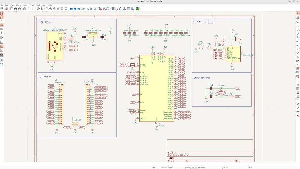
The schematic is basically a wiring diagram, that shows how everything will connect, but isn't like exactly where the components are placed or how thick your traces are, it's solely to show how everything is wired, not where.
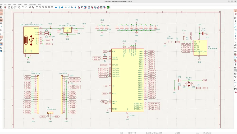
This is how are schematic will look when done the tutorial
The PCB editor is where you'll place down all your components and route everything for when you get it actually manufactured.
Starting the schematic
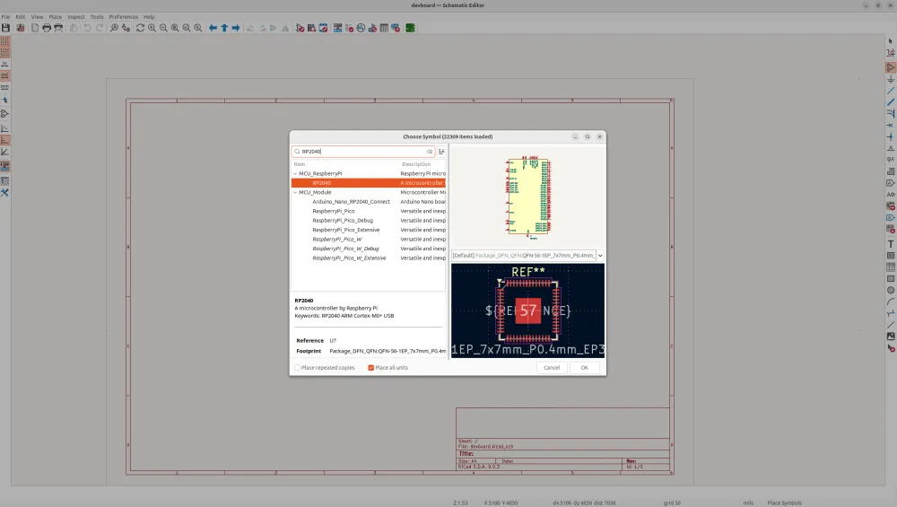
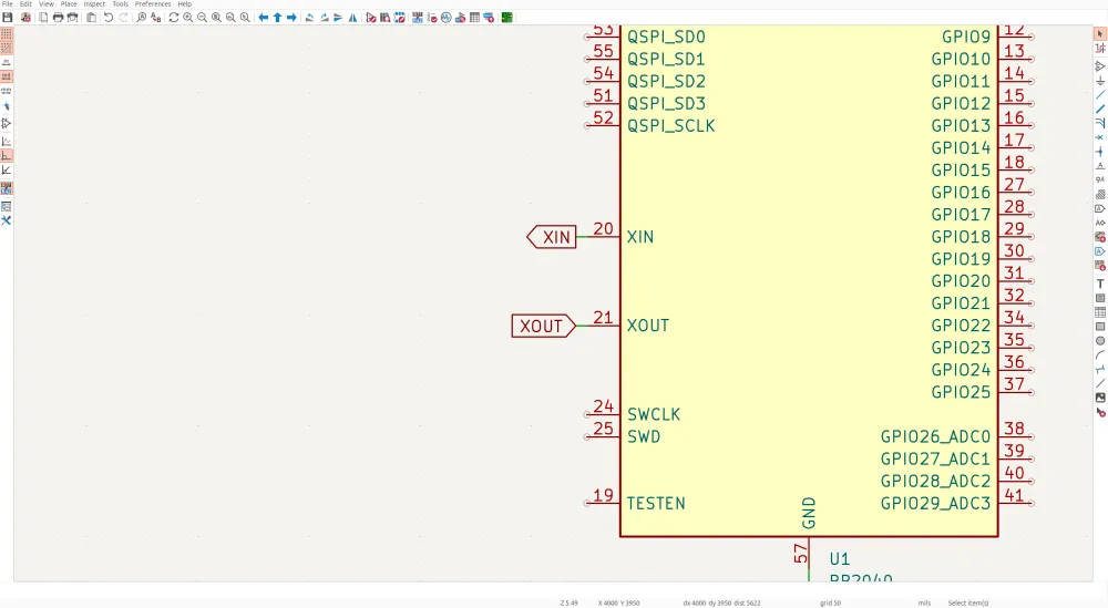
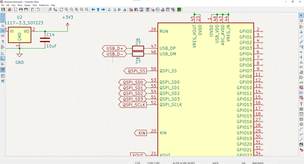
So enter in your schematic, and then tap "a", this will open up the symbol library, which is the place where you can find component blocks that you'll wire together to form the schematic for your project. Search for the RP2040, and just place it down in the center of your schematic.
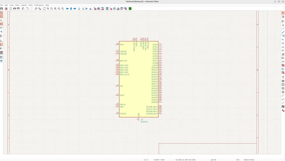
You'll notice the symbol and actual component are 2 different things if you look at the first screenshot. The symbol just tells you all the pins on the component, and how they'll be wired to what. The actual component has the physical pads where traces will actually connect to on your PCB!
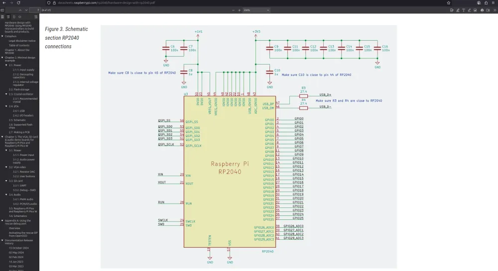
Our entire schematic will consist of 5 main elements: power, flash storage, the crystal oscillator, I/O (input/outputs), and your SoC, the RP2040! The Raspberry Pi datasheet explains how all of this will pretty much be wired, and I'm kind of just here to explain exactly how it all works too.
So first let's talk about power and some schematic good practices!
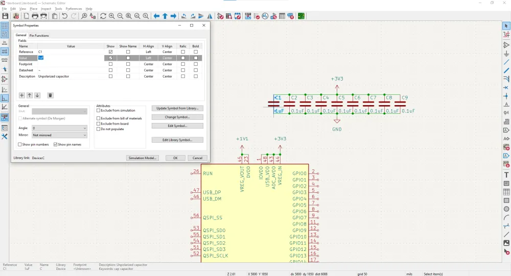
You'll notice that the RP2040 has capacitors, these are called decoupling capacitors. These capacitors are used for 2 main things, filtering out power supply noise and giving a local power supply if components need it at short notice. You can think of it like a stream of water, without the capacitors it can be jittery and unpredictable, but with the capacitors, the stream smooths out, making your PCB function more reliable.
You usually want to put one 0.1uF (or 100nF, the F stands for Farads) decoupling capacitor per power pin, but it's fine to deviate a bit from that, but that's the most optimal way of doing it and what we're going to do.
We're also going to put a 1uF decoupling capacitor on each power line. You'll notice that the RP2040 has a +1V1 (1.1V) and a +3V3 (3.3V) line, we want to put a 1uF decoupling capacitor per line, to act as a larger reservoir and to smoothen out larger ripples that could occur. With the RP2040, these 1uF capacitors are mostly to help provide a stable 1.1V supply. With this combination, we'll filter out nearly all the noise and have a smooth functioning PCB.
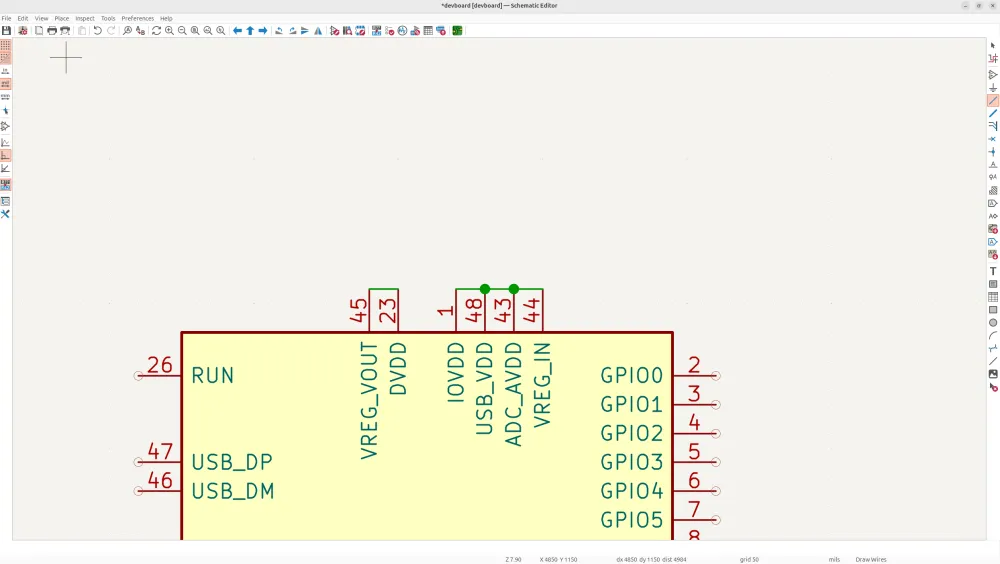
So go back into your schematic and then tap on the "Draw Wires" icon to connect the VREFVOUT and DVDD, and then separately connect the IOVDD, USBVDD, ADCAVDD and VREG_IN, because these pins have different voltages.
Now before we go further, remember that all power labels face UPWARDS, and all ground labels face DOWNWARDS, this isn't necessary for the schematic to work, but it's good schematic practices that you should always follow
Then tap "p" to open up the POWER symbol library (you can also tap a, but searching in p will be faster because there's less symbols), and search for "1V1" and "3V3" and place the 1.1V on the VREG_VOUT and DVDD, and 3.3V on the IOVDD and those other pins.
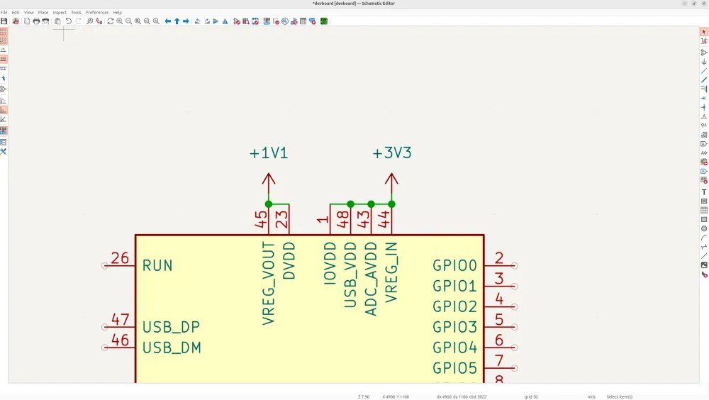
Now schematic good practices is to always put at least a small wire between symbols like this for clarity.
Now that we have our power symbols in, we're going to add the decoupling. You could technically wire them like the screenshot I showed before, but I prefer to separate them because you use less wire which I find looks cleaner, but it's up to personal preference, and readability.
You'll also notice that the symbol contains less pins than the symbol the RP2040 datasheet has, this is because symbols in KiCad tend to not repeat the same pins, so they just merge like all the same VDD pins into one.
But using the RP2040 datasheet as reference, we know that there's 8 IO VDD pins, so eight 0.1uF decoupling, and one 1uF cap because we're wiring the entire 3.3V line and need to smooth out the larger ripples. So let's just place all those in!
Again type "a" and search for "c" (the shorthand for capacitor). Make sure to double tap the capacitors to add a value, and make eight of them 0.1uF, and one of them 1uF.
These are the decoupling capacitors for the 3.3V line, now we need to do the caps for the 1.1V line. There's 2 VDD pins, so two, 0.1uF caps, and we need one for the line too, so a 1uF cap aswell:
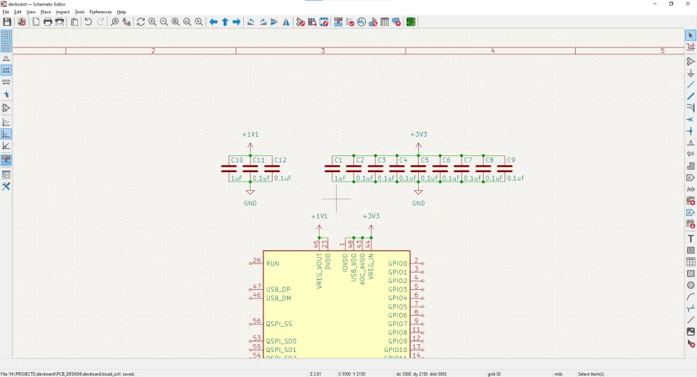
Now we have all of our power decoupling. We also need to connect GND to the SoC, this is pretty self-explanatory, but it allows power to actually flow properly in our PCB.
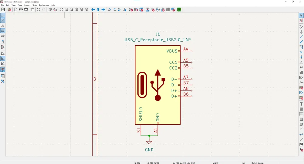
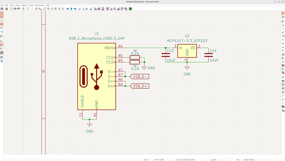
Working on USB-C
We have our power decoupling, but we don't actually have a power source yet or a way to program our devboard yet, so let's do that now. I'm going to be using USB-C because it's standard and fast!
So tap "a", type in whatever receptacle you want, and add it in. Make sure you pick "receptacle" and not plug because a plug would plug into your laptop instead of having a cable plug into it.
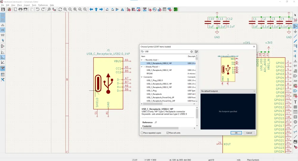
Now let's explain each of these pins:
- SHIELD/GND will both go to ground, shield is conductive material wrapped around the data pins on the receptacle, and this just improves EMI by grounding it.
- D+/D- are the data pins, these transfer data to/from the USB-C receptacle. You'll want to connect the D-'s and D+'s together so that they both transfer data.
- CC1 and CC2 basically tell the receptacle to allow power to go through to power the board. These by standard (the datasheet tells you) are pulled down (go to GND) through 5.1K resistors.
- VBUS is the 5V input, this will need to be stepped down to 3.3V to power our MCU (microcontroller)
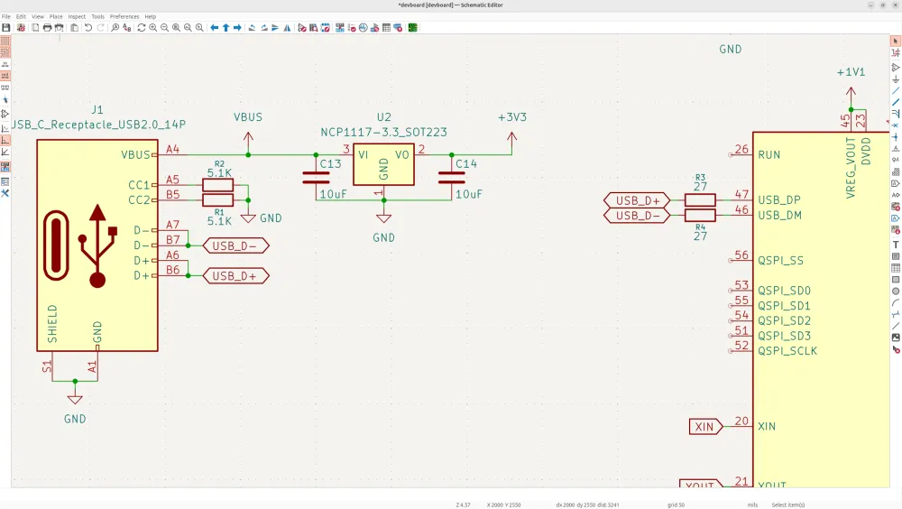
Now that we know what everything does, let's wire it up. Shield/GND go to GND:
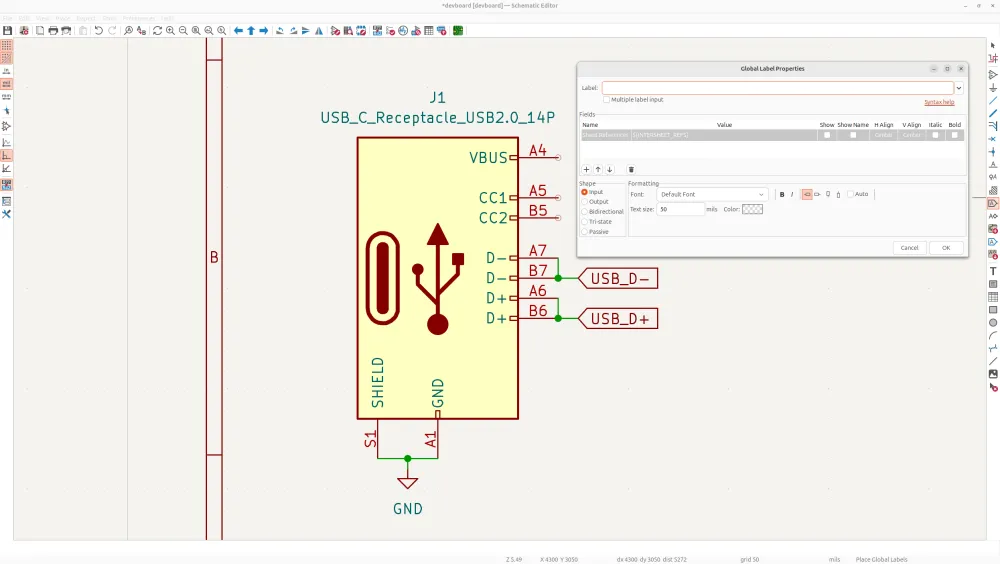
D+ and D- are attached to their relative pair, and then will go into the MCU, but for now, we'll just have a global label going out of them. Global labels are basically like little teleporters, that allow you to say that something is wiring, without manually putting a wire between them.
Technically global labels are meant to be used between different schematic sheets and net labels would be the correct thing to use here, but I find global labels are cleaner if you only have one schematic for your PCB.
To do this, tap global label in the right hand toolbar, type in the name for your label (USBD+ and USBD-), and add them to the pins:
Next, pulldown the CC pins through a 5.1K resistor to GND to enable power to go through the USB-C receptacle. Open up the symbol library, and then type "r" the shorthand for resistors, and then place it down and edit the value to be 5.1K:
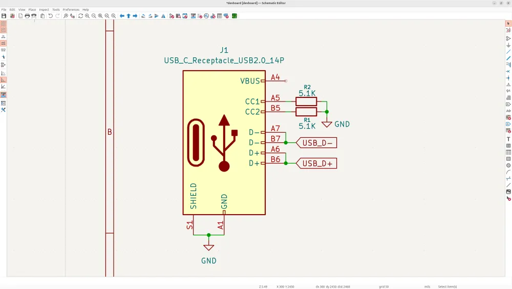
Remember to follow proper schematic good practices, and to have clearly visible values, and labels for your components. Feel free to edit the text of stuff to make your schematic cleaner, just don't make stuff too small.
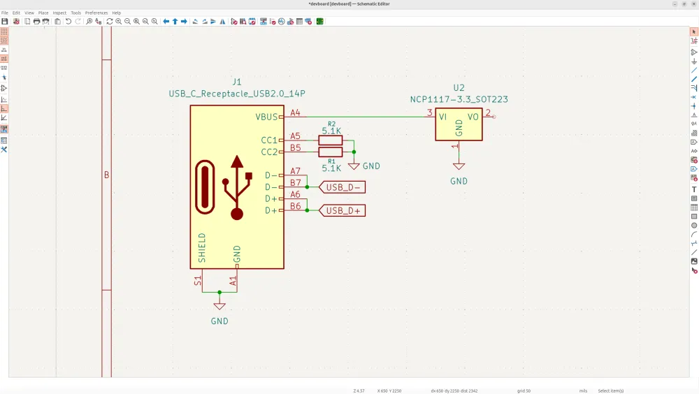
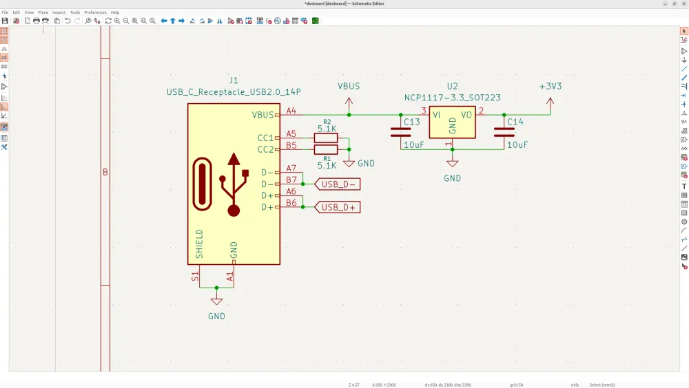
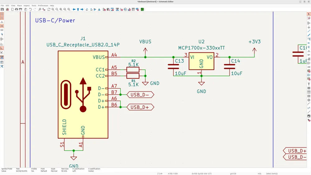
Now we just need to wire in the input voltage, but the thing is, the voltage of USB-C is 5V, while the voltage that the RP2040 uses as input, needs to be 3.3V so you don't cook it. To achieve this, we'll use what's called an LDO, or a Low-Dropout Regulator to take the voltage down.
Specifically, we'll be using the NCP1117, a classic and reliable fixed voltage regulator (I actually switch this regulator out later for the MCP1700, 3.3V, because it's really big on our PCB). A fixed voltage regulator is handy here, because we only need to go down to 3.3V instead of like 1.5V per say or something random, and it uses less components. We'll also be using the SOT-223 footprint (or package is the common term) because it's small and we don't really have any thermal issues with a devboard.
So add in the NCP1117-3.3_SOT223 symbol, wire GND and attach VBUS to the VI (voltage input) of the LDO.
Remember to always keep your schematic clean and feel free to use up quite a bit of space. Now like the decoupling capacitors on our RP2040, we need capacitors on the LDO. But we don't need fine decoupling capacitors for precise input lines into an MCU, and instead we need bulk capacitors, to handle the large voltage ripples when moving a voltage down.
So we need to place two, 10uF capacitors on each side of the LDO, for input/output, so add them into your schematic:
Next, we want to add our power labels to the LDO, we'll put a VBUS label before the LDO/Bulk cap, and a +3V3 label to the VO (voltage out) of the LDO. We might use 5V to power some other devices so we'll want to provide a power line for that too:
Now to finish off the USB-C wiring, we need to make sure the MCU receives the data lines. It's standard to have these going through 27 ohm resistors into the MCU to prevent distortions of the signals at high speeds, these are called termination resistors.
So wire the USB D+ and D- pairs into the MCU USBDP and USBDM (the P is for + and the M is for -) through 27 ohm resistors:
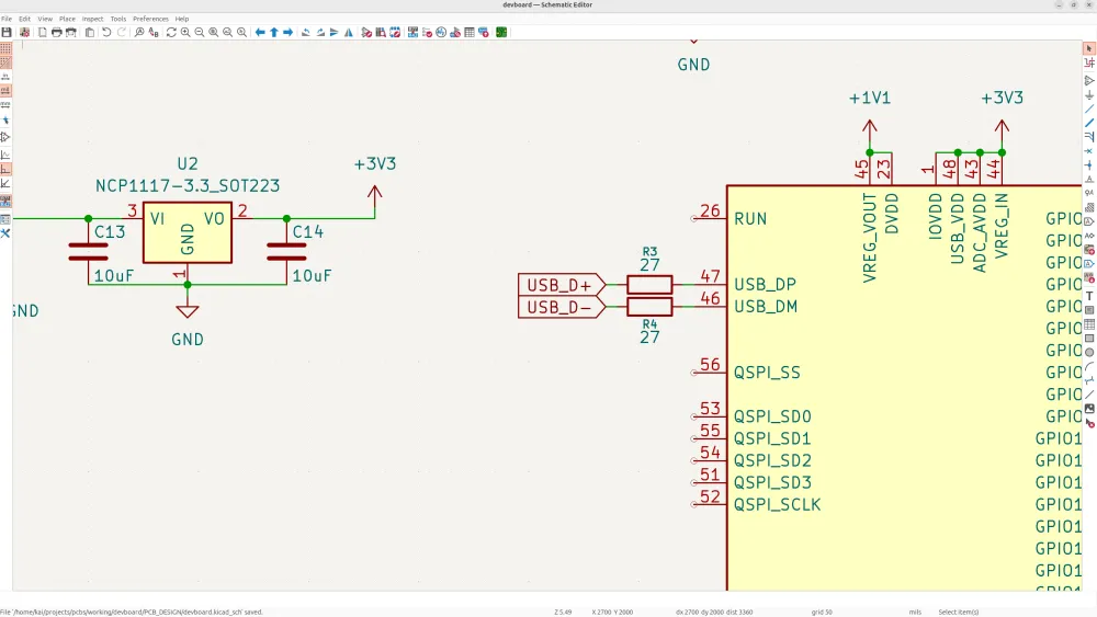
Now USB D+ and D- are actually what's called "bidirectional", this means that they work both ways. You don't actually need to specify this, but good schematic practices is to make sure your global labels reflect that. Currently they're just set as "inputs" because the triangle is facing inwards, so double click on all the D+ and D- labels and set them to bidirectional:
The crystal oscillator
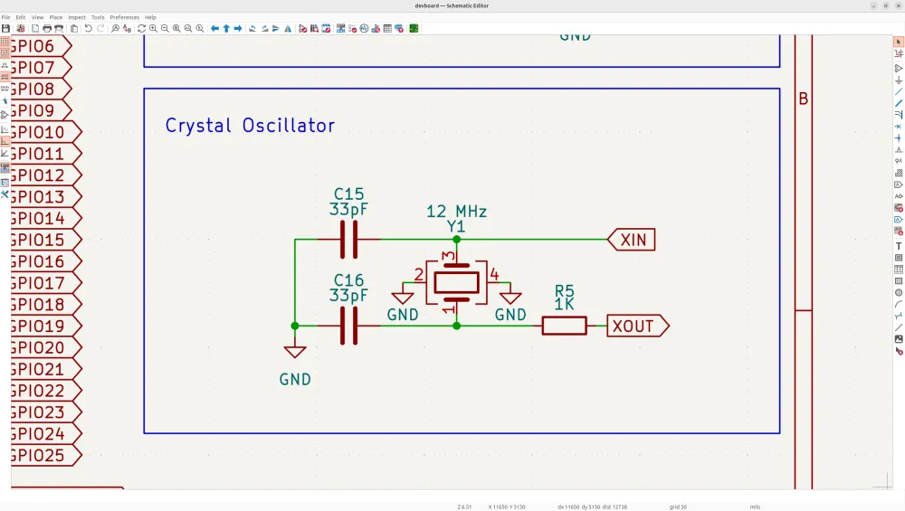
Now to make our USB and other peripherals actually work properly, we need to have what's called a crystal oscillator. This is a little piezoelectric quartz crystal that vibrates very precisely, and then it's amplified and fed into the MCU to act as a clock signal that controls the digital peripherals.
For example, you definitely want a crystal oscillator if you're using USB-C, because the data needs to come in at specific times, so it makes sure no data is incorrectly received. Because the clock is such a precise component, you want to wire it really carefully. That means it should be as close to the MCU as possible on the PCB (schematic doesn't matter, it's just a reference), and it needs really small capacitors, to smooth out the signals.
First add the global labels to the MCU XIN and XOUT, just called their relative name. XOUT is the output from the crystal so an input to the MCU, and XIN is an output from the MCU to help the crystal oscillate properly:
Remember to accurately represent your global label direction, but just keep in mind it doesn't actually change your schematic, it's only for whoever is reading it!
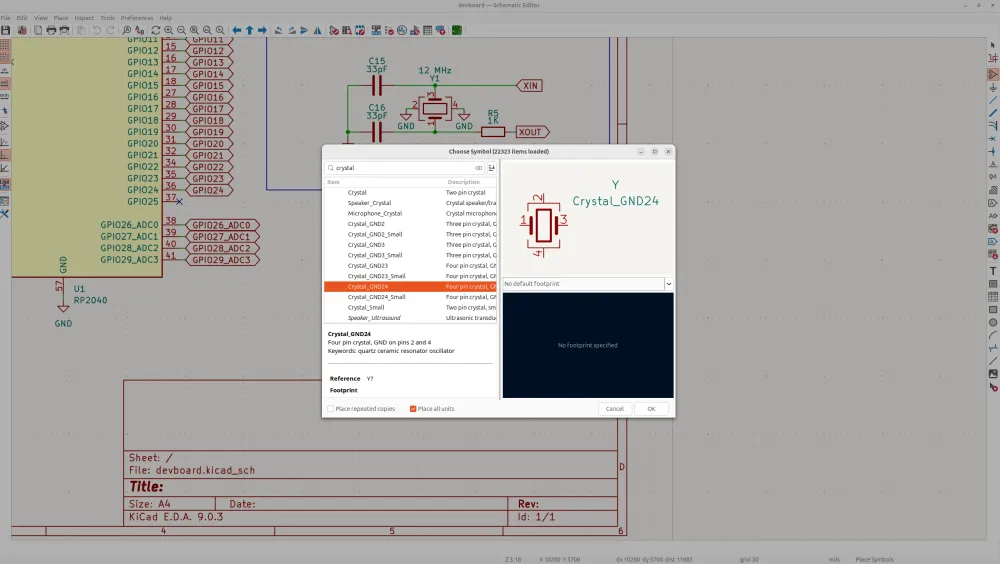
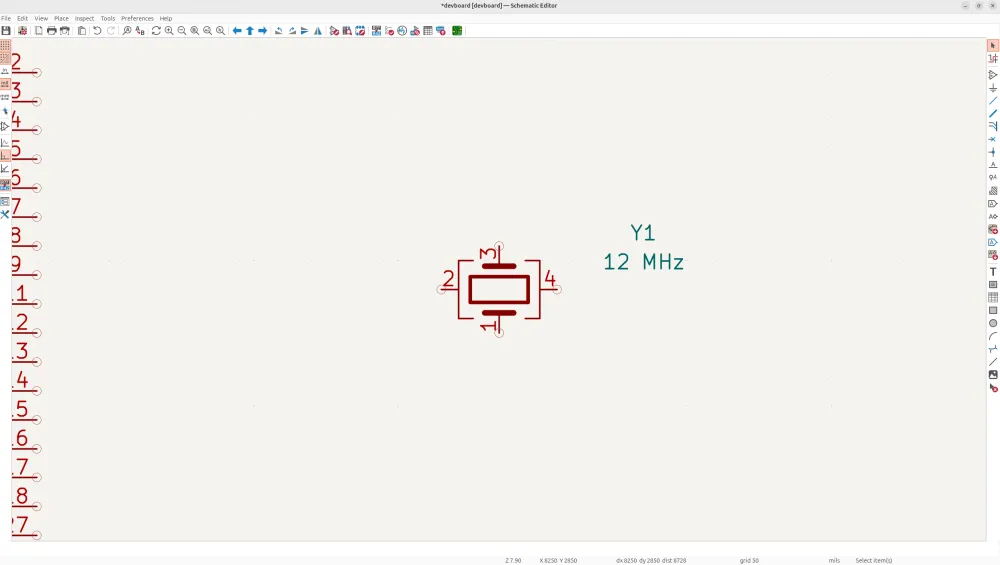
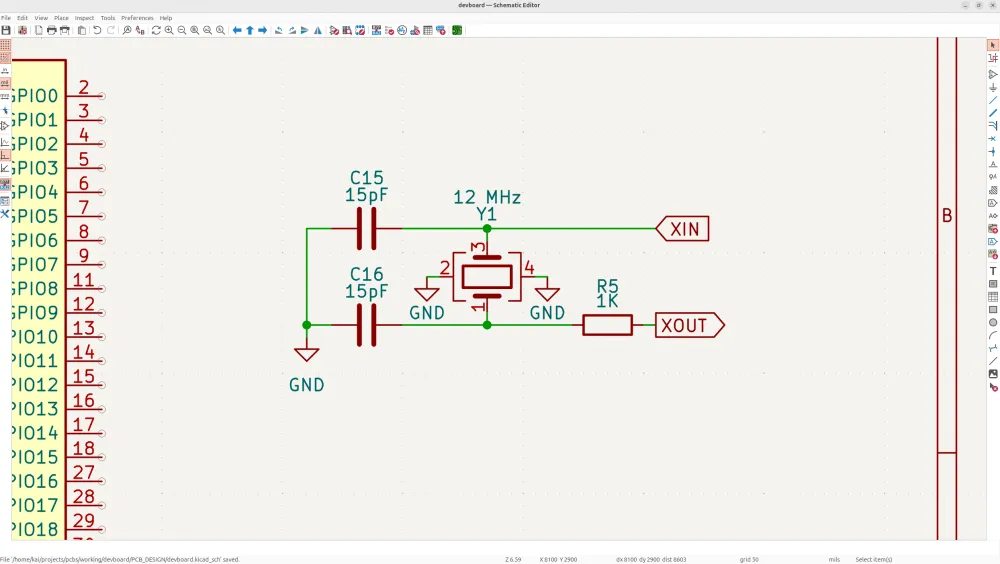
Based off the RP2040 datasheet, we're going to be using a 12 MHz crystal with two, 15pF (I switch these later to 33pF because we use a different crystal than the Pi Pico) decoupling capacitors. Make sure to use the crystal footprint with 4 pins and 1 and 3, as the input/output pins so pay attention to the symbol I use, and remember to change the name to 12 "MHz":
Pins 2, and 4 just go to GND, pins 1 and 3 need a 15pF cap in series, and XOUT will have a 1K resistor. This resistor is called a damping resistor and it prevents the crystal from being damaged and ensures good signal integrity:
Remember all your schematic good practices and make sure everything looks clean.
We haven't actually seen these types of caps yet, these are called external load capacitors, and they're placed in series with the crystal I/O's, these basically just ensure that the crystal resonates at it's proper frequency, I'd suggest researching a bit more if you're interested!
Flash storage
Now lot's of SoC's include flash storage, but the RP2040 actually doesn't, so we need to add on our own flash storage! You can think of flash storage as like a faster version of an HDD, with less power consumption, more reliability but is usually a bit more expensive.
Sadly, the RP2040 only supports up to 16mb of memory, so we'll just use a quad SPI flash memory IC (integrated circuit, those little chips on a board) like the W25Q128JVS used in the datasheet.
Now before we actually add it to our schematic, let's talk about what SPI is. If you continue to build PCB's, you'll see this communication interface very often, it's basically just a standardized way of transferring data. The signal comes out of the master, and then goes into slave devices. The master is our MCU in this case, and the slave, is our flash memory.
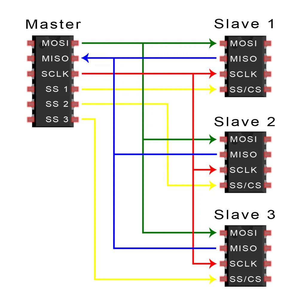
It has 4 major pins you need to understand:
- MOSI - Master output, slave input
- MISO - Master input, slave output
- SCLK - Clock signal (remember that oscillator we added to our board, this will basically do that for other devices)
- SS/CS - Slave select, let's you choose what device you're communicating with
So you usually need to have all 4 of those, and then you can add SS pins as you wish if you want to communicate with more and more devices.
But we're actually using quad SPI in this case.
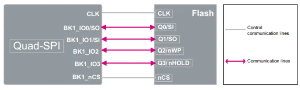
Quad SPI uses the same CLK and CS pin, but has 4 IO pins, so it can transfer data, 4x as fast as SPI, which is ideal for flash memory, but it does take up more pins, so that's why it's not always used.
Now you can't just attach SPI to any GPIO, you have to use what's called a hardware controller, which you can imagine, is like a little block on the RP2040 SoC that is specifically meant for SPI. There are 2 SPI controllers on the RP2040, so we're going to use them for our flash memory. You can also technically do SPI via software, but it just makes way more sense to use the actual controller provided.
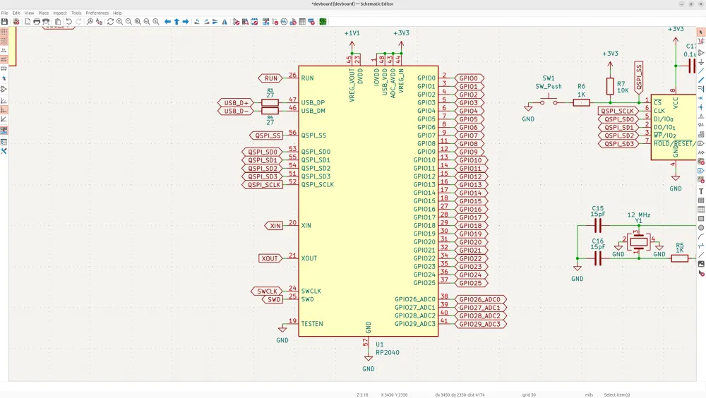
So add a global label to the QSPI pins with their relative name, IO's are bidirectional, and CLK and CS/SS are inputs to the slave (the flash memory) or outputs from the MCU.
Next, add in our flash memory IC (chip), W25Q128JVS, and wire up all the QSPI pins, and put GND to GND, and VCC to 3.3V:
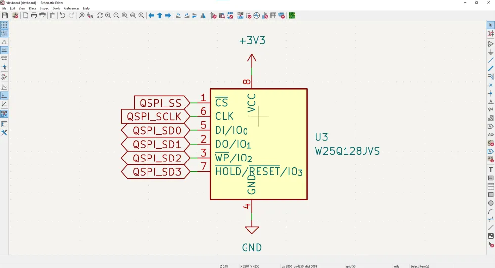
Next, we need to add our 100nF/0.1uF decoupling capacitor to our VCC line to filter high-frequency noise. And then, we're going to add a button to the CS line, so that we can enter what's called BOOTSEL mode.
Based off of the RP2040 datasheet, if the QSPI SS pin, see's a 0 or GND when it's booting up, it'll go into BOOTSEL, where it will appear as a USB device on our computer so that we can copy code onto it to set it up.
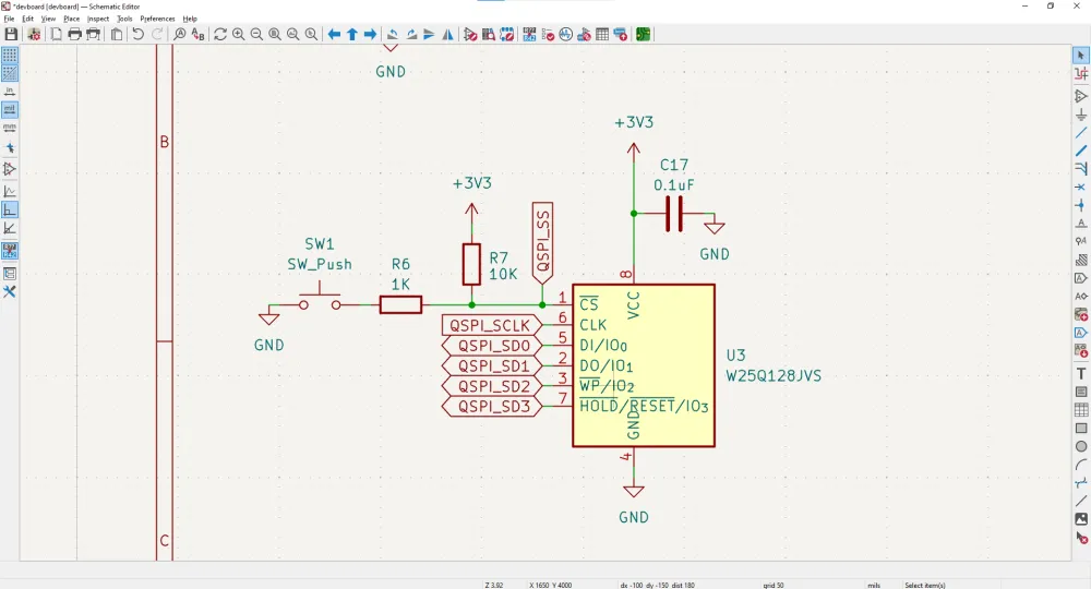
Now there's 2 resistors you're probably wondering about here, the pullup to 3.3V, and the one in series with the button.
The pullup to 3.3V is important, because usually the QSPI pin will show up as 3.3V to the flash memory, but during bootup, you can't guarantee that it will, because the pin isn't active, so you might have some weird thing that happens with your board. The 10K resistor is just standard that the RP2040 datasheet wants us to use (and is also pretty commonly used to filter noise and stuff).
The 1K resistor in series limits the amount of current that can flow in this part of the circuit to prevent damage to the CS pin.
And just like that, we have our button and decoupling in, and our flash memory is completed!
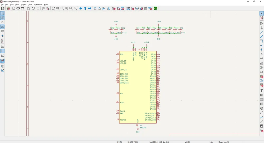
Breaking out I/O Headers
Now we have all the components for our board to actually work, so we just need to breakout all the GPIO's on the RP2040, onto header pins so that we can use them in our circuit and whatnot!
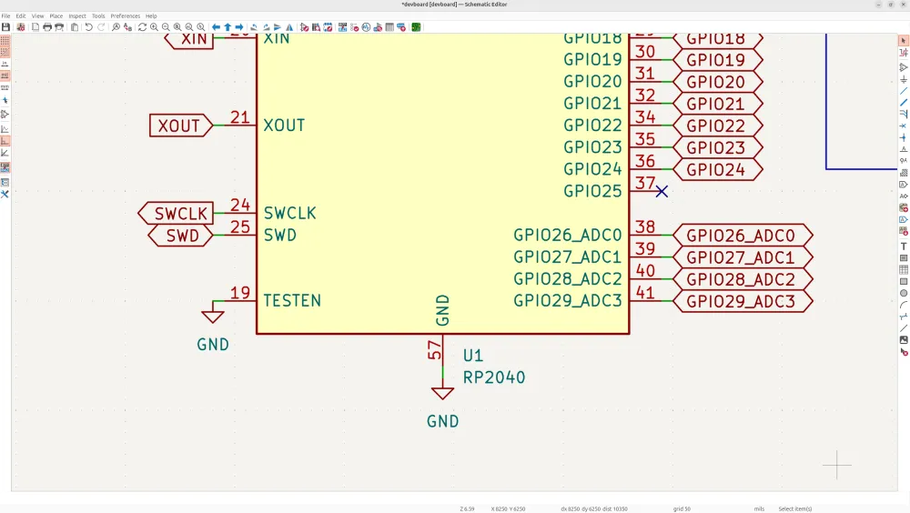
But before we do this, let's just make sure we attach TESTEN to GND on the RP2040, this pin is just meant for factories to make sure that the RP2040 SoC actually works before sending them out.
Next, we'll label all the other pins we haven't broken out (all the GPIO's, SWCLK and SWD), with their relative name on the RP2040. These are all bidirectional pins except the SWCLK pin, which is a clock output from the SoC:
I actually labelled mine the wrong direction for the rest of this tutorial, but it's purely cosmetic and won't actually impact my PCB, this is how it should actually look:
Next, we're going to add the actual header pin symbols into our schematic. You can technically do this whoever you want, but I'm going to adhere to the raspberry Pi Pico pinout:
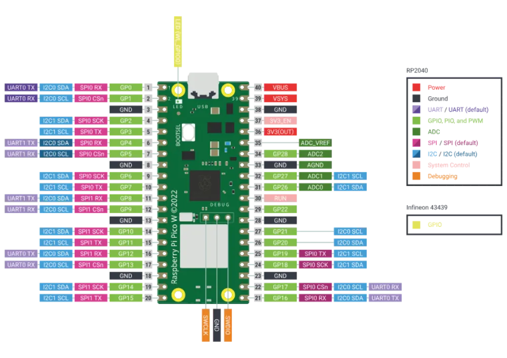
So add in a two, 1x20 header pin symbols, and one 1x3 header pin symbol, I just used generic symbols, but you could use pin header symbols if you want, it's just up to preference:
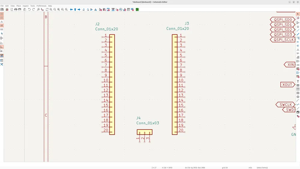
Usually you don't want to make your symbol layout look exactly like your PCB, but I think it makes it more obvious so that we don't mess up our pinout!
Next, we'll just add in all the pins, and we'll just leave out the ones we don't know yet like VSYS, 3V3EN and ADCVREF, I'll explain those after:
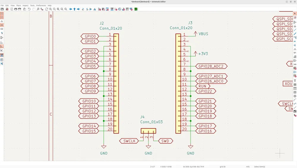
Now the Pi Pico can actually be powered by a battery, but we're not implementing a battery (if you want to, check out the Pi Pico datasheet), so there's a diode on the VBUS power line, so they have a VSYS line after the diode and a VBUS line before it, but because we don't need a diode, we don't need VSYS.
This also means we don't need 3V3EN, and then ADCVREF is kind of just another thing to give a reference voltage to ADC, but it isn't really necessary, and we're just making a simple devboard so we won't use it.
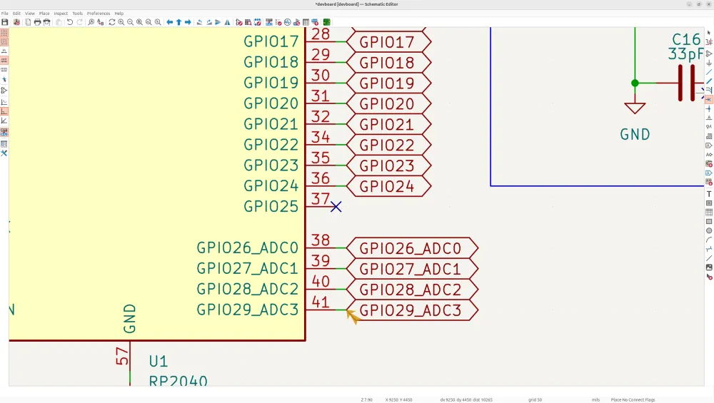
Because we have these free pins, and also some GPIO's still left, let's just fill these pins with some GPIO's. I'm going to move the ADC pins up, and then fill the other pins with GPIO's. I also want to use GPIO29 which is an ADC pin and replace GPIO25 with that just so we get the added ADC pin:
Because of this, you'll want to just no-connect GPIO25 on the MCU, just to tell KiCad and others that we're not using that pin:
If you want to add battery support, you can do so yourself, but I'm keeping to a minimum framework. And just like that, we have all of our header pins in!
Finishing up the schematic
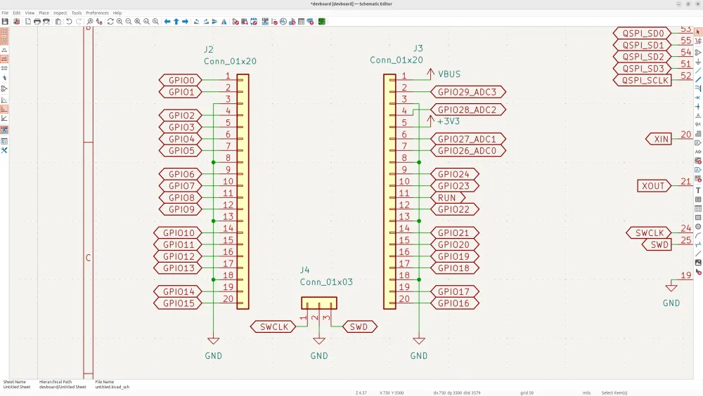
Now that we have our I/O headers in, we're actually finished with all the symbols in our schematic, this is how your schematic should look:
Now to organize our schematic, even more, let's separate our design into different blocks using the text boxes in the schematic editor. When doing this, you usually want to place your component blocks by flow of your PCB. So if you could image, power flows in through the USB, so we'll put that in the corner, the MCU should be center because it's the fundamental of the PCB, and then the other stuff can just be organized around:
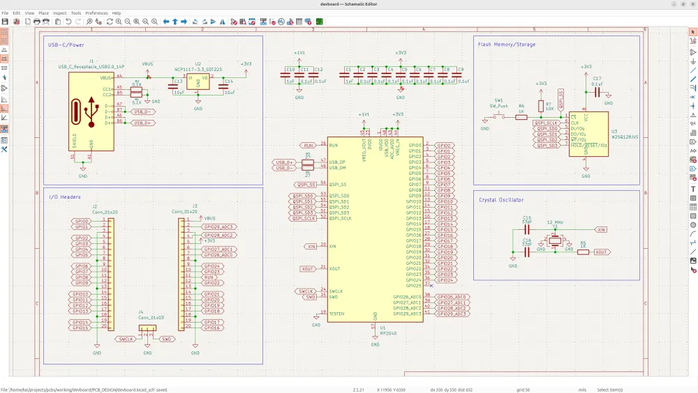
You don't have to do this, but I feel like it keeps everything nice and clean!
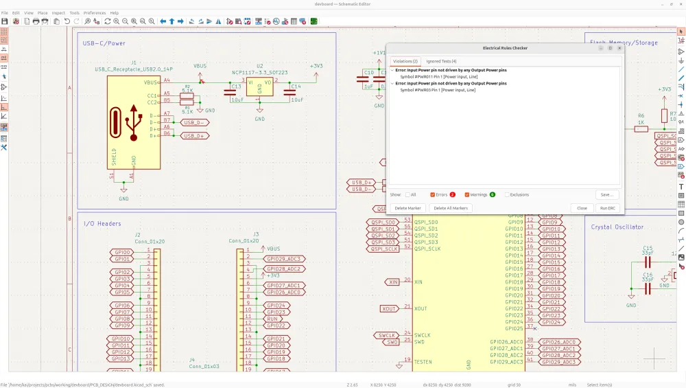
Next, run ERC to just make sure you don't have any unconnected or weird stuff happening in your schematic. The only error you might get is Input Power pin not driven by any Output Power pins. You can just ignore this error, it's basically just the fact that we're labelling our power as bidirectional, and with no input/output, but we know that the MCU takes in 3.3V and that the USB-C outputs 3.3V, so we're totally fine to ignore it.
Footprint time!
Now that we've finished out schematic, we need to start working on the actual PCB. The first thing you need to do for the actual PCB, is to add in all the footprints for your components.
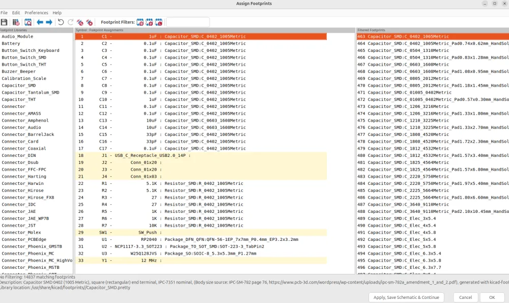
A footprint on a PCB basically just defines it's pads, outline, etc, that your component needs in order to be solder able on a PCB. So just tap on the assign footprints tab in the top toolbar to open up the footprints tab:
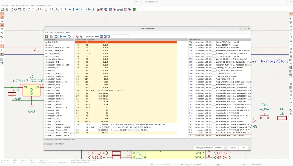
Now before we add in our footprints, let's talk about standard imperial sizes of SMD components, and SMD vs THT components.
So if you don't know, there's SMD components, which are surface mount, which means that the components are attached to the surface of the PCB like caps, and then there's THT components, which are soldered through the board, these are things like the headers.
For SMD footprints, you'll want to understand what the imperial sizes are:
- 0402 are the smallest footprint we'll have on our PCB, these are tiny footprints and anything smaller than this becomes too small to easily solder, these are good for low current applications, and are fine for our fine signal decoupling.
- 0603 footprints are a bit larger than 0402, and are better for slightly higher current and will maintain better physical stability for the larger decoupling needed for 10uF caps and such.
- 0805 footprints are pretty large and are really just needed in higher current applications, we won't be using any of these because we don't have any crazy large caps/components
So all of our 0.1uF/1uF/resistors will be 0402, and then the 10uF caps will be 0603, so just filter in the search bar for 0402/0603, and choose the resistor/capacitor footprint for the relative component:
Now these other components need to usually be found on LCSC and then you go into the datasheet to find the footprint, and then add it in, but I'm decently experienced and know what footprints to use already, so you can just copy what ones I'm using or find your own if you want and add them in:
These are my thought process behind the other components, JLCPCB has what's called basic and extended parts, and extended parts cost $3 each to add to a PCB because they have to be loaded into the assembly machines, this will be important here:
- USBCReceptacleHROTYPE-C-31-M-12: JLCPCB doesn't have any basic part USB-C receptacles, so I just chose this one I kind of like from a previous board. PART
- PinHeader1x20P2.54mm_Vertical: This is just the proper size header pins we need, they should be through hole/THT to be stronger instead of SMD, I mean if you wanted to, it could be SMD though. The part is just pin headers I'll buy separately
- SWPushSPSTNOAlps_SKRK: This is a small SMD size button footprint found in the JLCPCB basic library, so it doesn't cost anything extra and is pretty compact. This isn't actually the EXACT footprint, but it's close by like .1mm, and I found it by just scrolling through footprints with some filters. PART
- CrystalSMD3225-4Pin_3.2x2.5mm: I found this crystal on JLCPCB basic parts, and looked at the datasheet to find the footprint. You really have to make sure your crystal footprint pinout is proper because lots of people accidentally use the wrong footprint or symbol. PART
Now we actually need to modify our crystal schematic a bit because of the part we chose on JLCPCB has a load capacitance is slightly different, so we actually need 33pF caps. You can just search up the math if you want to learn how to do this:
And just like that, our schematic and footprint selection is finished, so we can actually get to the real fun stuff.. the PCB!
Let's design a PCB
Now that all that stuffs done, tap the switch to PCB editor button on the far right of the top toolbar!
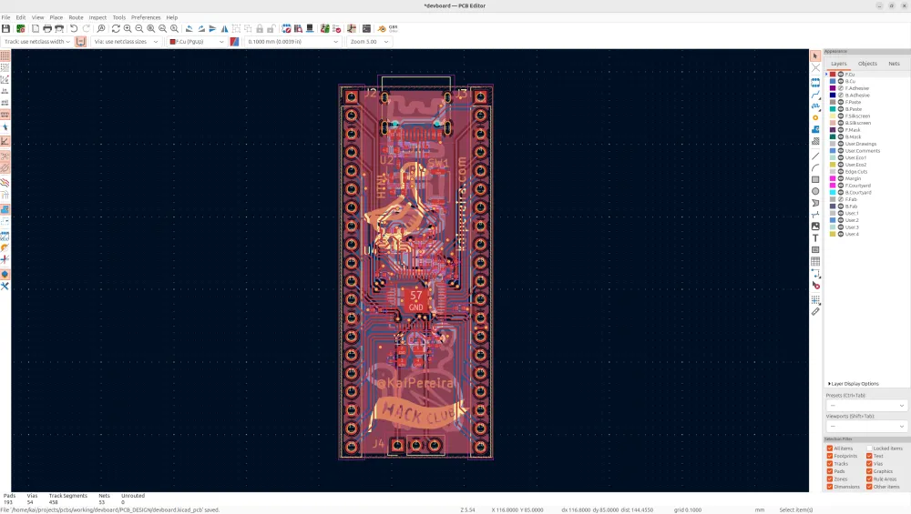
This will bring you into a new editor you haven't seen yet, this is where we'll actually place down the components on our PCB, and route everything.
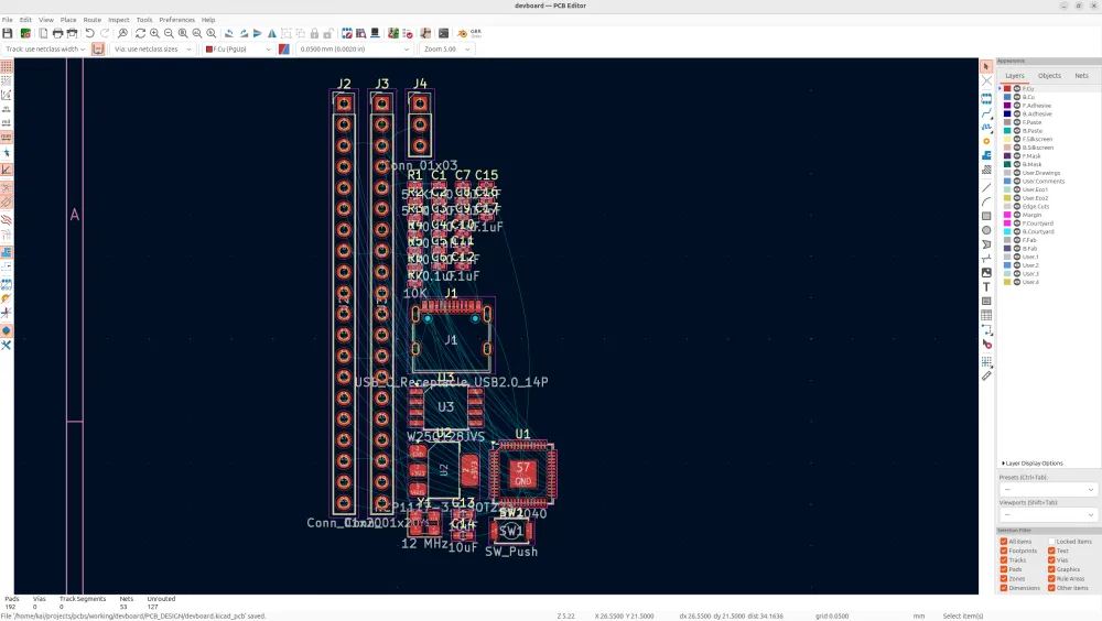
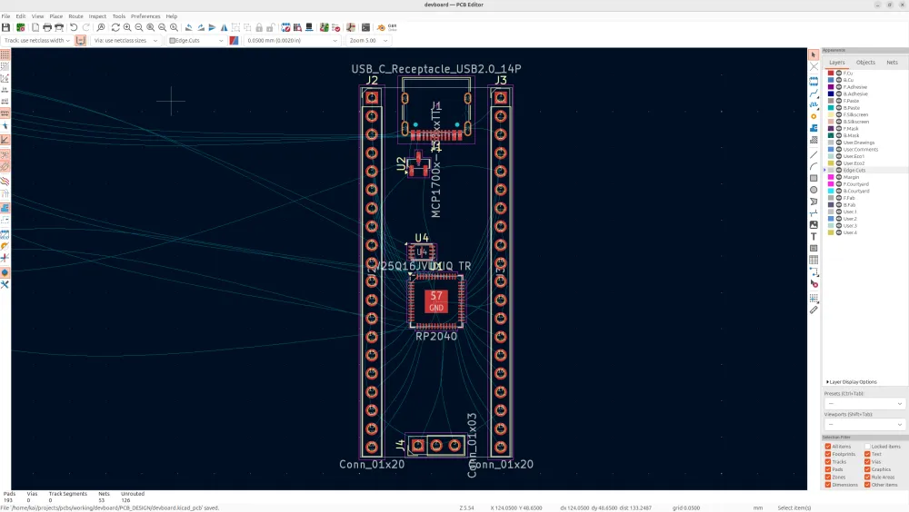
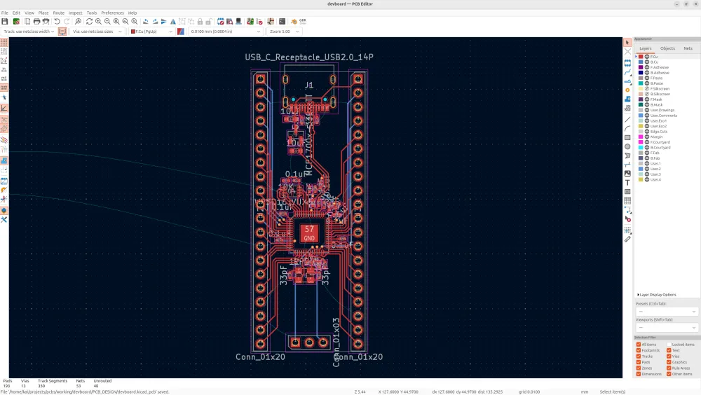
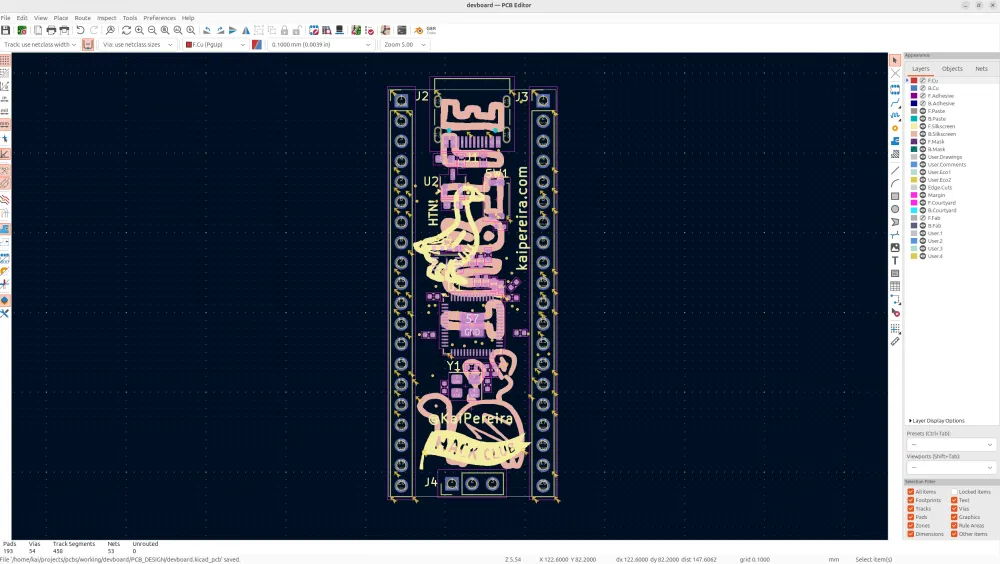
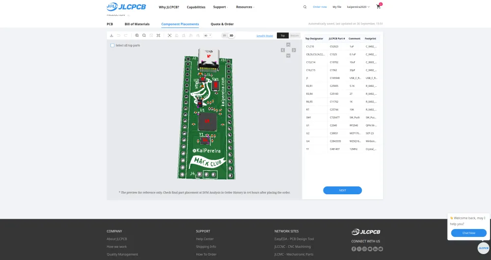
So in the top toolbar, tap the update PCB from schematic or F8, and then tap the update PCB button that shows up, to bring in all the components into your PCB, and just put them all in the top left corner of your PCB:
You might get some warnings which can be ignored usually (I just got some pin warnings which are fine), but there shouldn't be any errors.
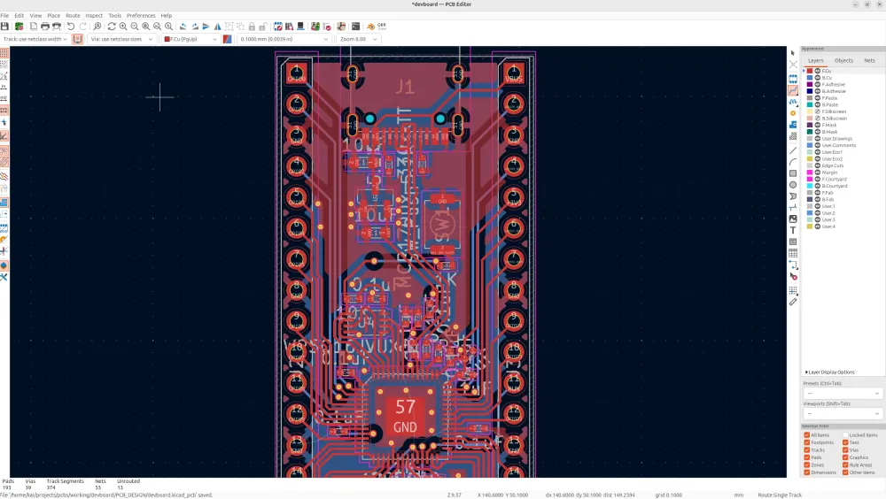
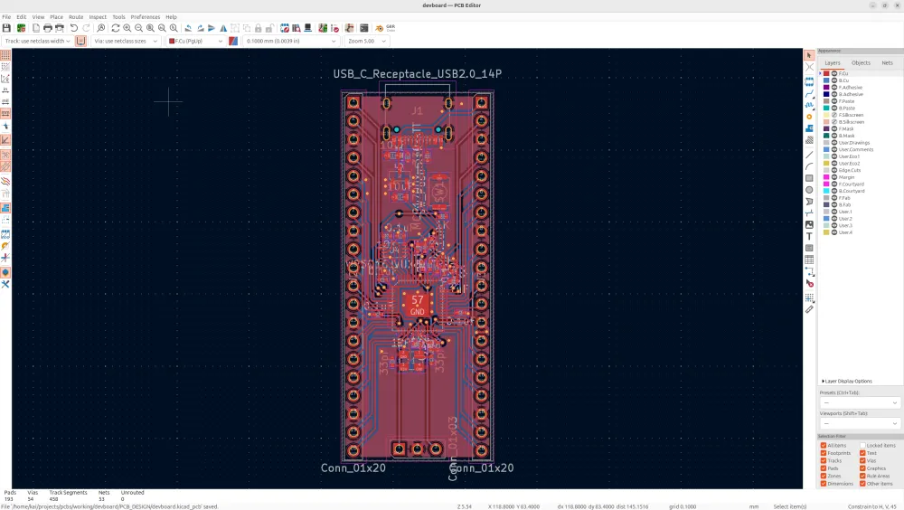
Now you'll see our actual components on the PCB, our USB-C, the RP2040, the button, crystal, LDO, flash, headers and our caps/resistors!
PCB Layout
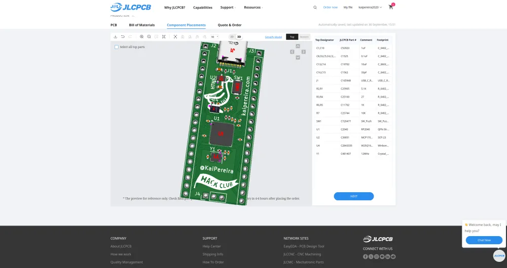
Now before we actually lay out all of our components, we need to define our PCB outline, holes, etc. So using the datasheet as a reference, we'll place down everything accordingly. Start with the board outline, and then do holes and stuff.
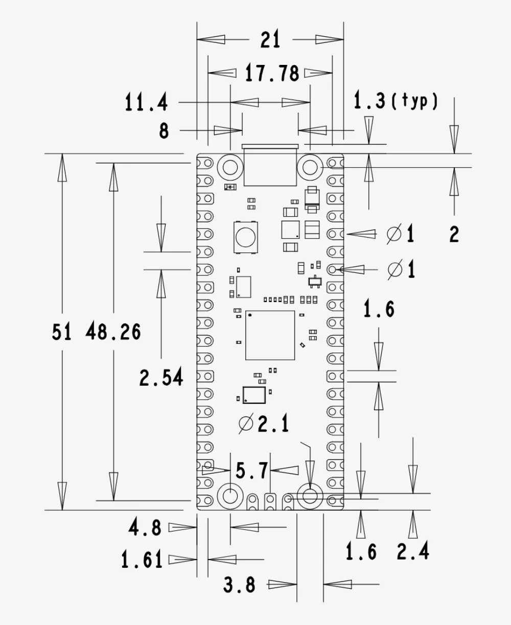
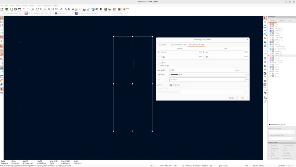
To add in a board outline, tap on the Edge.Cuts layer and then tap on Draw Rectangles, and then just put whatever size rectangle you want. After that, we'll add in the proper size from the datasheet, which is 21x51mm, so tap on the rectangle, then tap "e" and use the By Center and Size tab to do this:
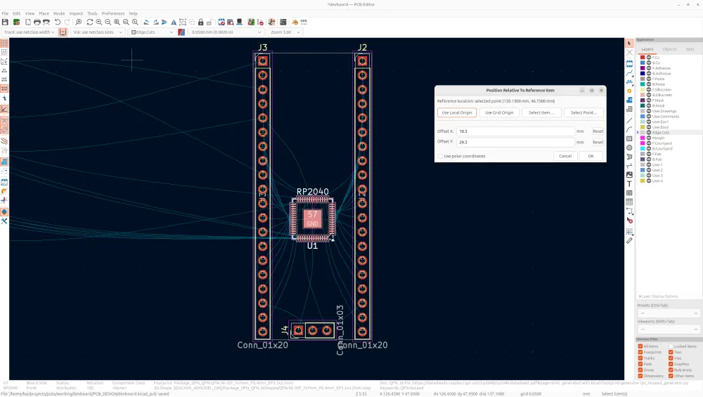
Next, we'll align the header pins onto our PCB by using the position tool. So right click on one of the header pins, go Positioning Tools -> Position Relative To, and then go Select Point and tap one of the top corners of the board outline. And then using the datasheet, align the X to 1.61/-1.61 based off of the side, and the Y to 1.37:
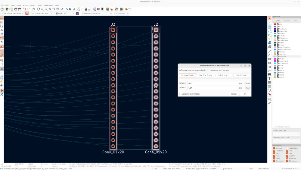
(I actually misaligned my header pins in this screenshot which I fix later, but just put J2 as the first header, and J3 as the second one, so it's easier to route)
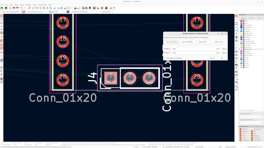
Next, we need to put our bottom header in, these are aligned to Y -1.61 and the X should be centered so 7.96 (10.5 is the center, minus 2.54 the pin spacing), and use the bottom left/right as reference (make sure it's flipped horizontally when aligning):
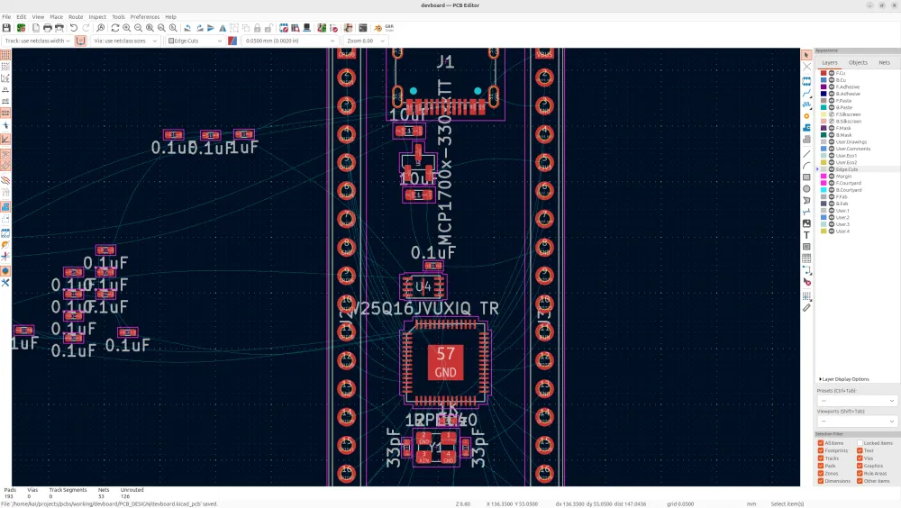
Next, I'm going to put in the RP2040 dead center, but with the Y slightly farther down, because there's more components above the Pico than below, so I want a bit more space for signals, I'm going to put it down an extra 4mm, but you can do how much you want.
Then, I'm going to center the USB-C, down a bit to the top of the devboard:
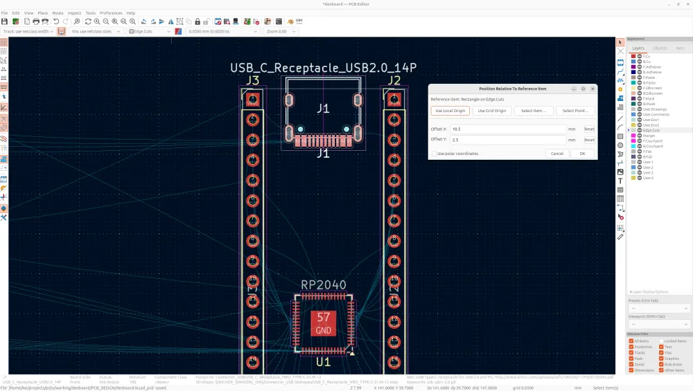
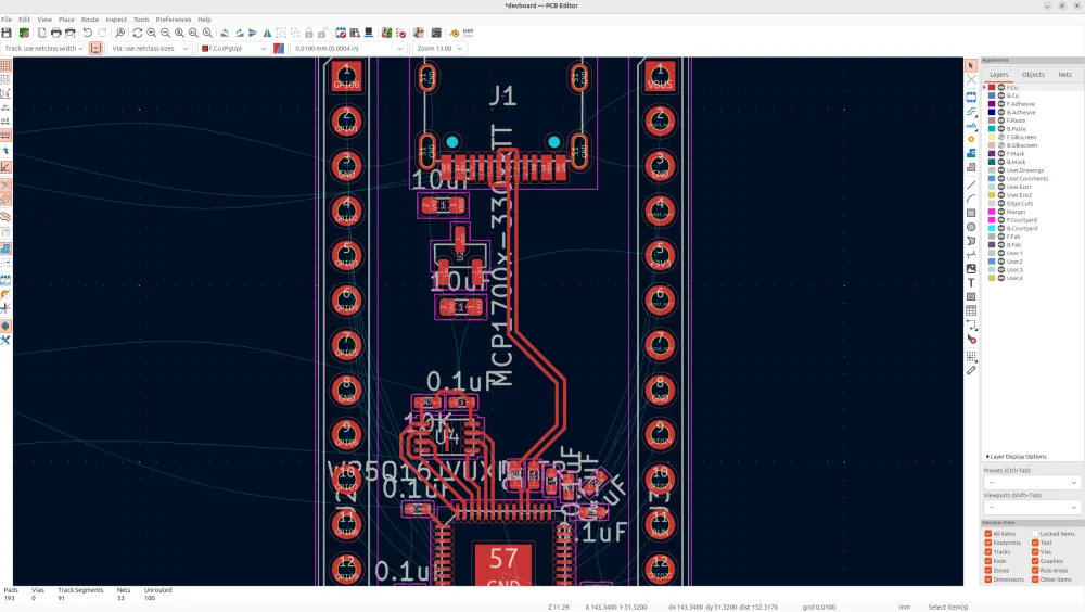
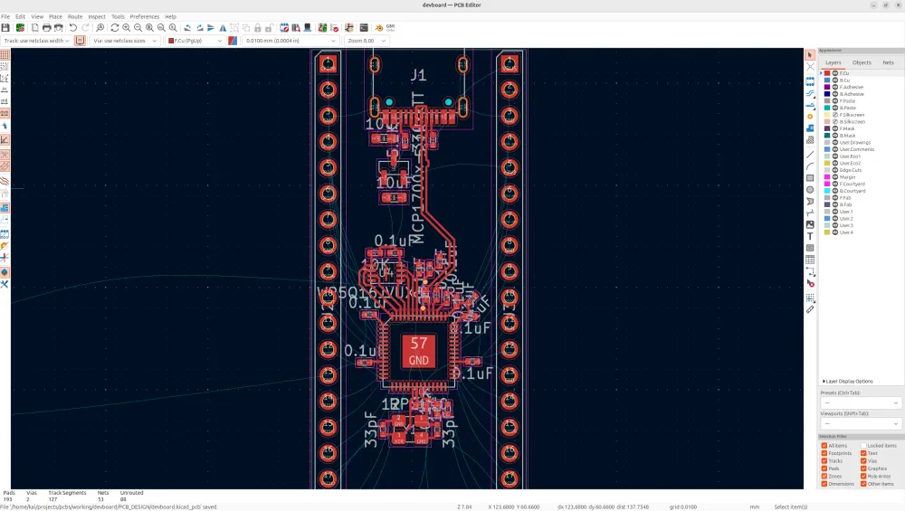
Now looking at the flash memory and LDO IC, they're really big, so let's use different components for them:
I'm going to switch to the MCP1700 LDO, which is smaller, but does handle less current (250ma), so if you plan on drawing more current, you might want to use a different LDO. So just replace the NCP1700 with the MCP1700x-330xxTT (this means tapping 'a' and searching it, not just the name of it because this one uses a smaller footprint!):
And then, we're going to change the flash memory to what the Pi Pico uses and has a slightly smaller package, which is the W25Q16JVZPIQ TR and uses the PackageSON:WinbondUSON-8-1EP3x2mmP0.5mm_EP0.2x1.6mm footprint, which isn't the exact footprint, but should work fine:
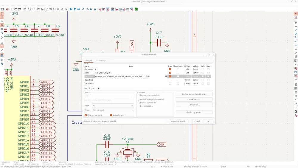
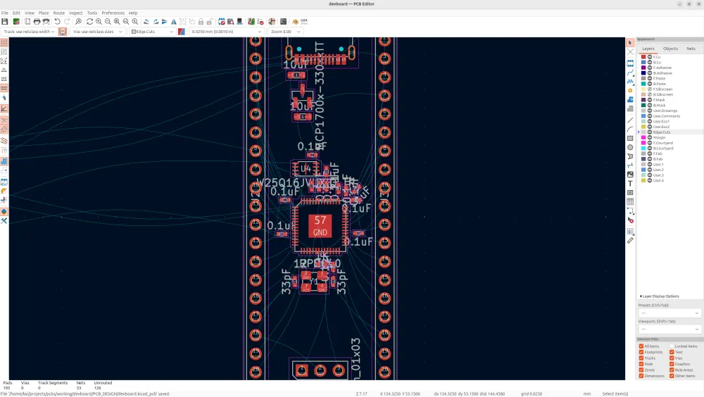
Now your footprints should be much better:
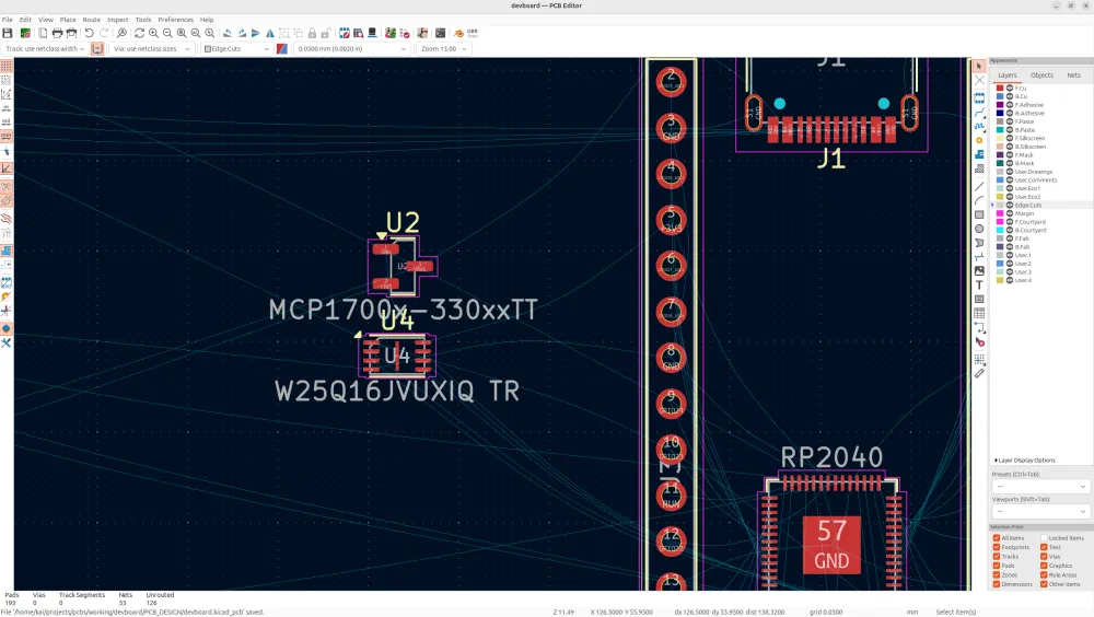
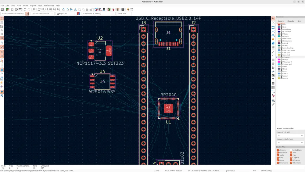
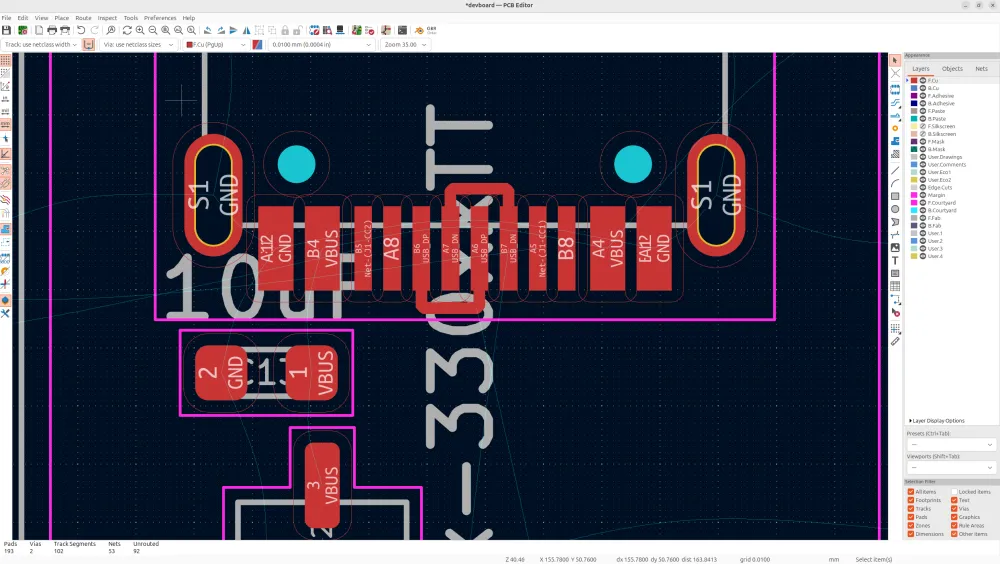
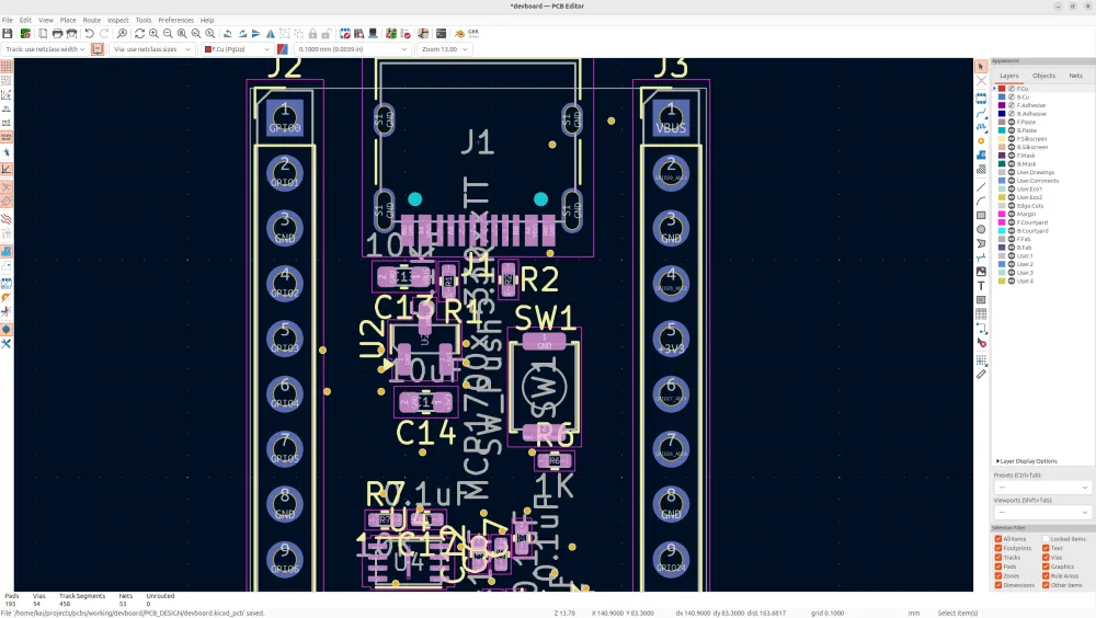
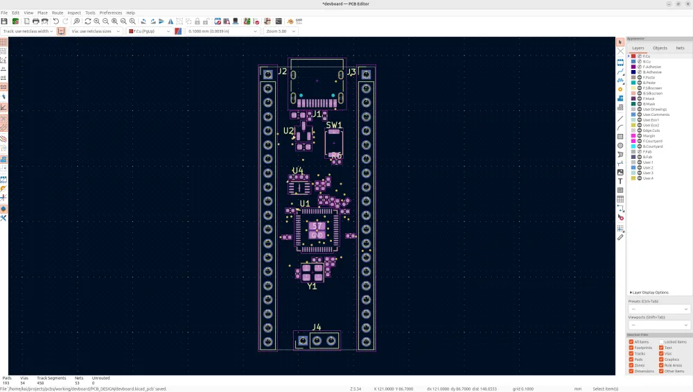
Anyways next, we're going to organize our parts onto the PCB (I also fixed my header pins and MCU orientation in this step). The LDO is going to go really close to the USB-C VBUS, and the flash storage will go close to the RP2040's QSPI pins:
I use exact positioning when doing things like this, but you can just draw them on if you want, I just like everything to be nicely symmetrical.
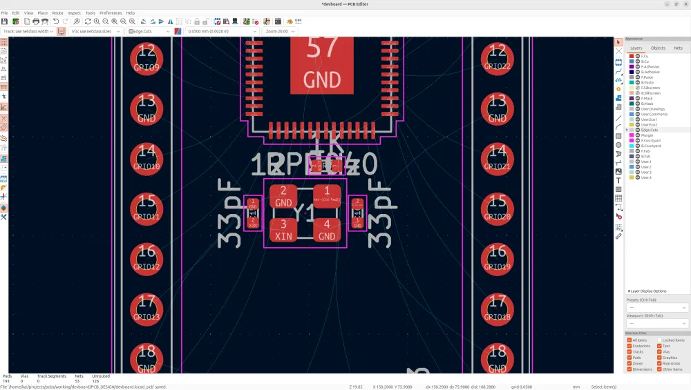
Next, I'm going to put the crystal on. The crystal should be very close to the RP2040 XIN/XOUT pins because it's a very precise signal, and the load capacitors should be RIGHT next to the pins too. You can then just put the resistor right by the XOUT pin of the RP2040:
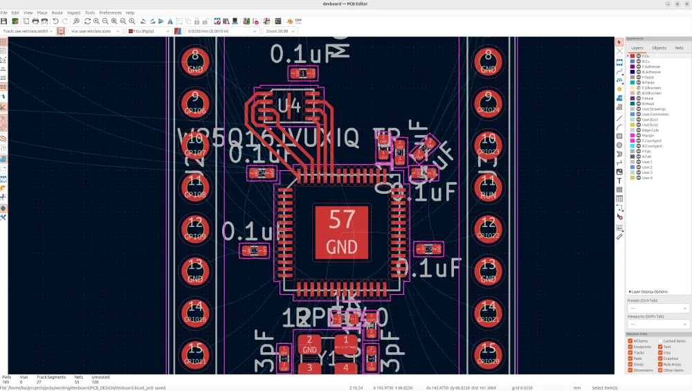
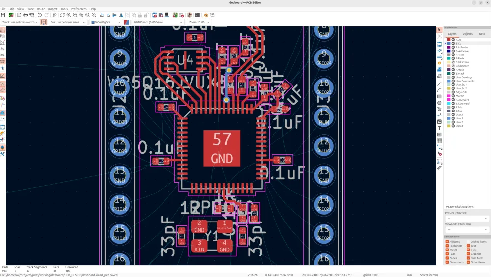
Now I'm going to put all the decoupling capacitors on my board. Decoupling capacitors should be as close as possible to the pins they're decoupling, the larger the cap is, the farther it can be, but try to keep them close to their pins.
Also feel free to mess with layout a bit during this step just so everything fits in efficiently! Try to use whatever capacitor you used in your schematic for organization purposes.
First I usually group all the caps that go together, and then I usually either start with the SoC caps, or components caps, I'm going to start with the components caps:
Remember, caps go by whatever they're decoupling. Now all the RP2040 caps are grouped together, and this is because it's just a general rule to have one cap per VDD pin, and then the larger cap/bulk cap near the group of them:
This is the layout I decided on, some of my thought process for this layout was:
- Leave enough space to route the USB differential pair
- Be able to route QSPI without via's for fast signals
- Leave enough space by the crystal to be able to route those traces
And I'll still definitely actively update it while I route my traces, but this is a good starting point.
Now all that's left to add in, is our resistors, but I'm going to actually put these to the side, and start routing a couple things! This is because it's going to be easier to place components not in the way of where traces are going to go.
Not before we start routing, remember a couple key things about routing:
- Never have a trace at a 90 degree angle, these mess with your signals, and also sometimes get manufactured weirdly
- Think about what you're going to route next, so that you don't route where that trace needs to go
- Know what you're routing, things like decoupling caps need to have short, small traces, etc.
- Never put via's on pads, this makes it hard to solder them, and makes the component unstable
- Try to route front signals vertically, and back signals horizontally, this isn't a fixed rule, but just try to do it in most spots to have efficient routing
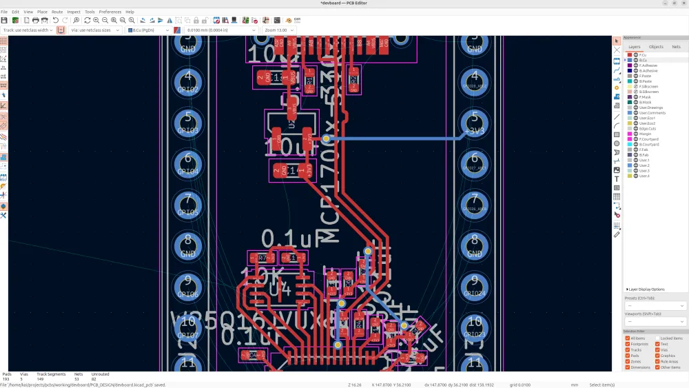
So, the first thing I'm going to route is my flash memory, I'm going to move the capacitors away temporarily while I do this and then add them back on later. So tap on the route single track in the right hand toolbar, and then route all the signals like so:
I usually start my route from the RP2040, and then put it into the component just because I find it's easier. I always start with routing my higher speed signals, and then do the lower ones.
Next, I'm going to route the USB-C data lines. Now these lines are actually special on our PCB, these need to be routed as differential pairs, basically perfectly even traces, next to each other. This is because they're carrying high speed data, so the traces need to be the same length so that data arrives at the same time.
The termination resistors for these data lines also need to be right by the RP2040 pins to smooth the signals. These also need to be placed perfectly evenly apart, centered on the pins so it's easy to route our differential pairs:
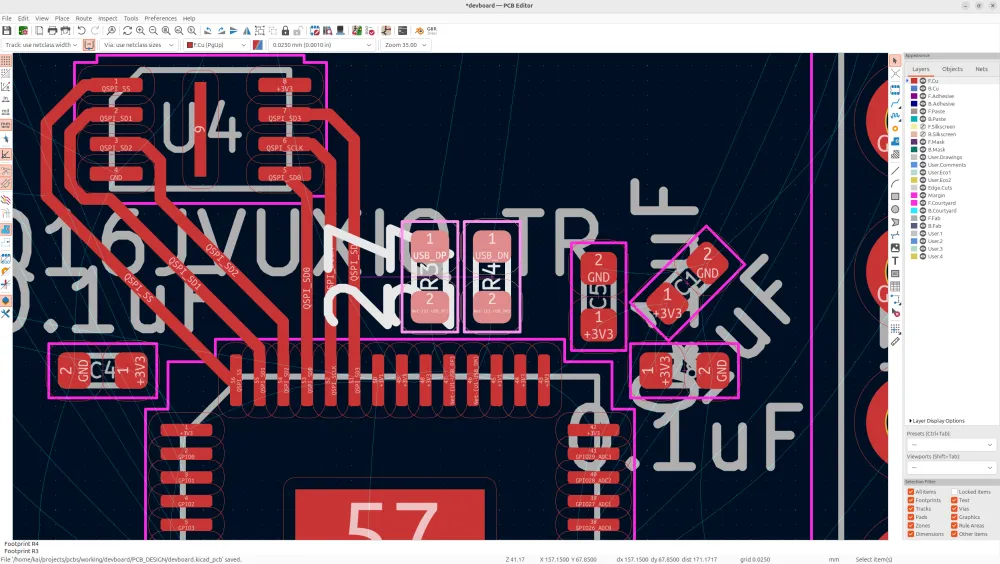
Now to route a differential pair. First wire the USB D+'s/D-'s together:
Then, hold the route tracks button, and go over to the symbol with 2 traces on it, or just tap 6. Then, go over to your USB-C, and tap on one of the D+/D- pins to start the trace, and route it down to your resistors. If the traces won't go into your resistors pads, that means that your resistors aren't evenly positioned, you can just the relative positioning tool to do this.
And then you can just route the resistors nets into the RP2040 nets (Make sure they're centered so the traces are the same length, you could technically do this as a differential pair if you change your schematic slightly, but it's fine if you just position properly):
I added left a space inside of the USB traces for the decoupling capacitors to go.
Now we need to make sure all these traces are the same sizes, you can check the resistor traces by using the Tune length of a single track tool on the right toolbar, they should be the same length if you did it right:
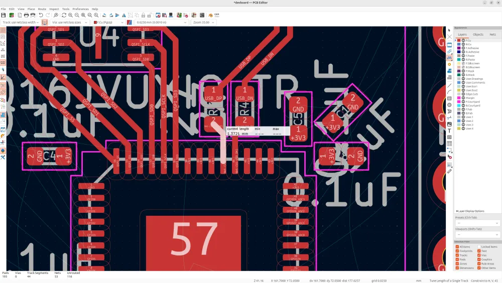
And then, your USB-C lines, are probably not the same length, so we need to fix that. You can do that by going to route -> Tune skew of a differential pair in the top menu, and then selecting the trace with a negative skew, and just tapping it, and then tapping ok, and it should make it slightly longer:
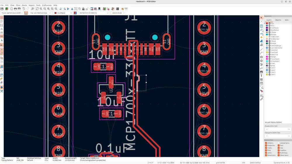
This makes all of our traces the exact same size, so that we have proper data flow!
Now we just need to wire the extra pair of D+/D-'s on the USB-C to the route that we already have. Just wire these directly
Now that we have our fast signals on the PCB, the other signals are fine to go through via's, so we can put in our decoupling caps now:
Leave all of the grounds for last, I'll explain this soon
Now my routing of course isn't perfect, but I did manage to get it pretty nice and tight. You'll notice some blue on the PCB, and that's me routing on the other layer. You can change layers by tapping the other layer on the right layers view, or by tapping V. But for SMD components, you'll need what's called a VIA in order to get to the other layer, which is essentially just a hole. Feel free to use the backside for routing if you don't have any space!
Anyways, next I'm going to route the crystal, the USB-C pulldowns, and button pull ups, and then I'm going to leave the button/button resistor for very last because there's no specific spot that needs to be:
Next, we're going to route power to our board, I'm distributing power to the main cluster of VDD pins, and then once I'm finished routing the other signals, I'm going to route it to the other pins, just so power is even about my board:
Now, wire every single header pin on the board, try to keep organized when doing this, and save via's/the other layer for last:
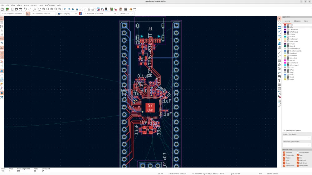
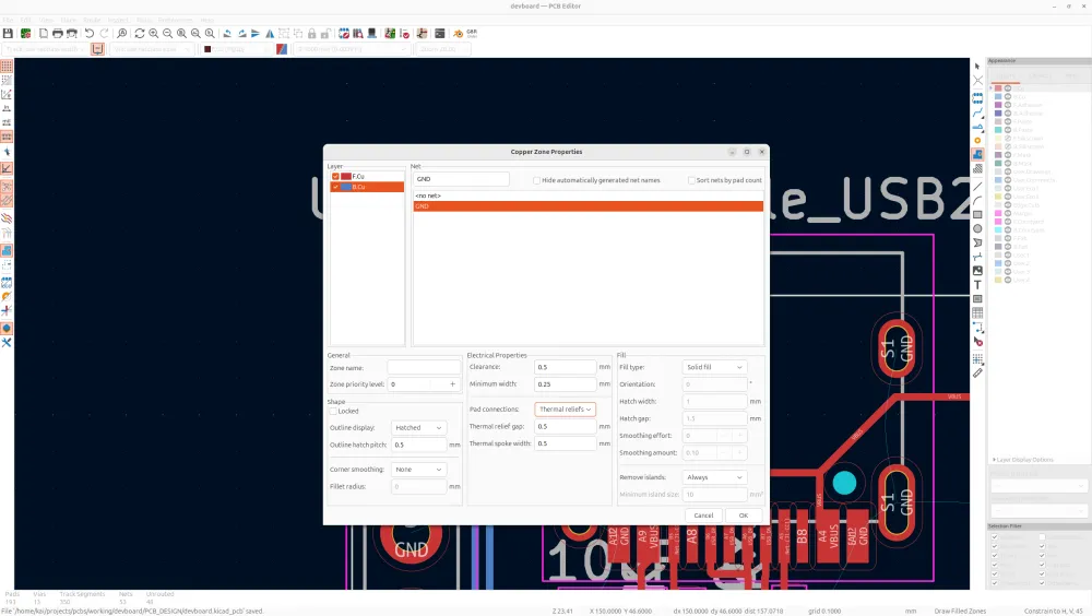
And with a bit of finesse, all of our routing is pretty much done, we just have all of our ground signals left. Now you're probably wondering why we didn't route those. Well instead of using wires to do those, we can use what's called a ground fill.
This is basically like a giant pool of just ground on our PCB that connects all of our grounds together. We do this because it helps with signal integrity, and because there's always going to be a lot of ground signals on a PCB. It also helps with thermal regulation!
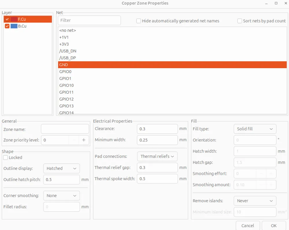
So on the right toolbar, tap Draw Filled Zone, and select both layers, with GND as the net, and select Thermal reliefs as the Pad connections. Basically, with a ground fill, soldering can become harder because the fill dissipates heat, so doing thermal reliefs puts like less ground area to the hole so it's easier to solder stuff on!
Then, select the entire PCB with your ground fill, and then tap B to fill it:
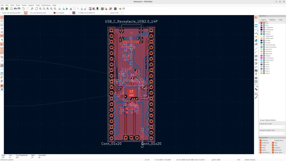
Now you'll notice that all your ground ratliness disappear. Their might be a couple that are still there though, this is because the pads are isolated, so you might need to put a via from the pad onto the ground fill. You also might need to adjust like some of the header pins signals and such to make it work!
I'd also suggest adding via's to all the isolated islands of ground for signal integrity, but this is just good practice, and also putting extra near the SoC and stuff that get's hot like the LDO:
Next, we'll need to add in our button that we haven't put in yet. Just find a free spot on your PCB for it, I'm going to put mine near the flash memory though because it's got some space and it's a close connection:
And then, if you just have any ratlines still on the PCB, just connect them up, and you'll be on the final step of designing our PCB:
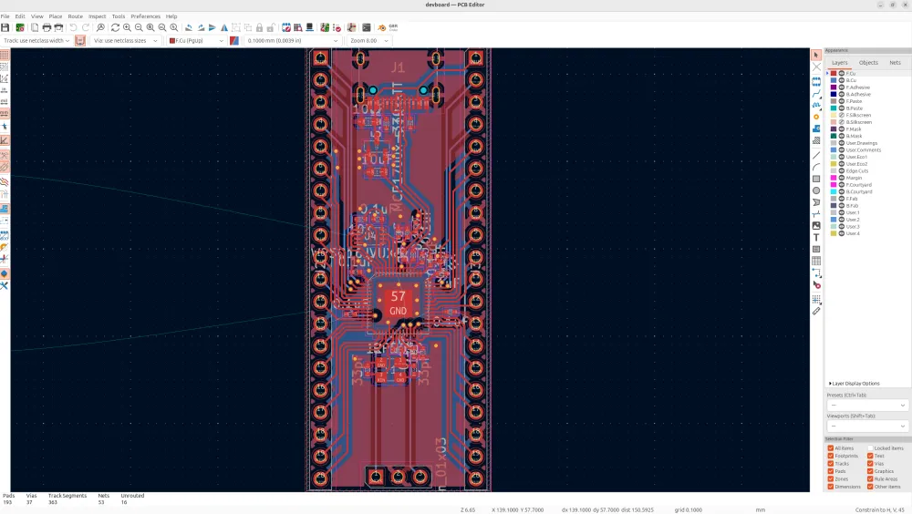
Now you probably think, we'll we're done the PCB, what else could there be, well there's actually a couple more things we need to do. The first thing is running DRC to make sure there's no problems with our PCB. So go to the top toolbar, and run DRC:
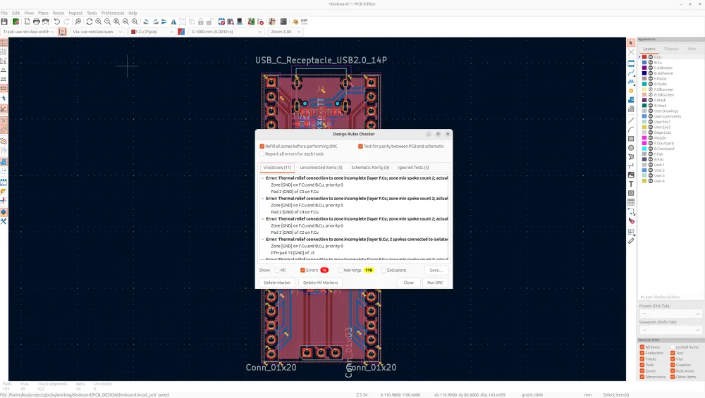
My PCB has 16 errors, yours might have more, but all of these need to be properly resolved. The first things I'm going to look at is my unconnected items. These just tell me what I forgot to route, so make sure that you get all those fixed first.
Most of these are problems with the ground pour, so I'm actually going to modify the ground fill to fix a lot of these errors, I'm changing the thermal relief gap and clearance to 0.3mm instead of 0.5mm which just makes it so the traces and pads can be closer to the fill:
You'll probably also have a bunch of thermal relief errors. These require some finesse to fix, but essentially you just need to have like a thick enough ground on each component. And you can solve this by adding via's, traces, and a bunch of other stuff like editing the fill. So you'll need to research a bit and try different things to fix these. And not all of them are even too crucial, but I'd suggest fixing them all.
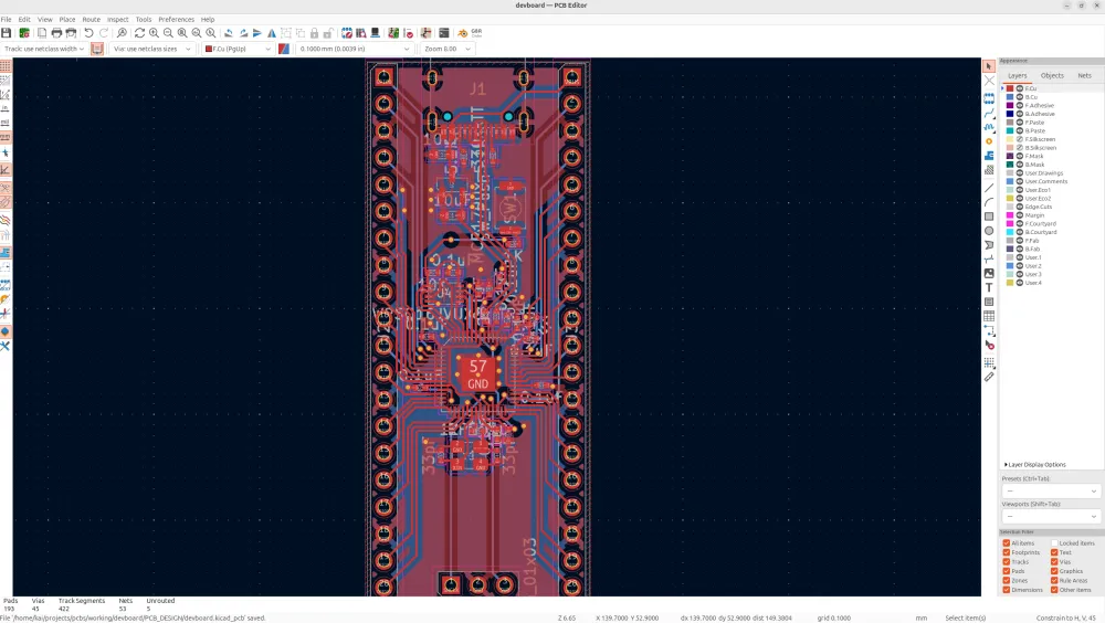
The rest of the DRC errors you'll have to figure out, but here's how mine looks with no errors left:
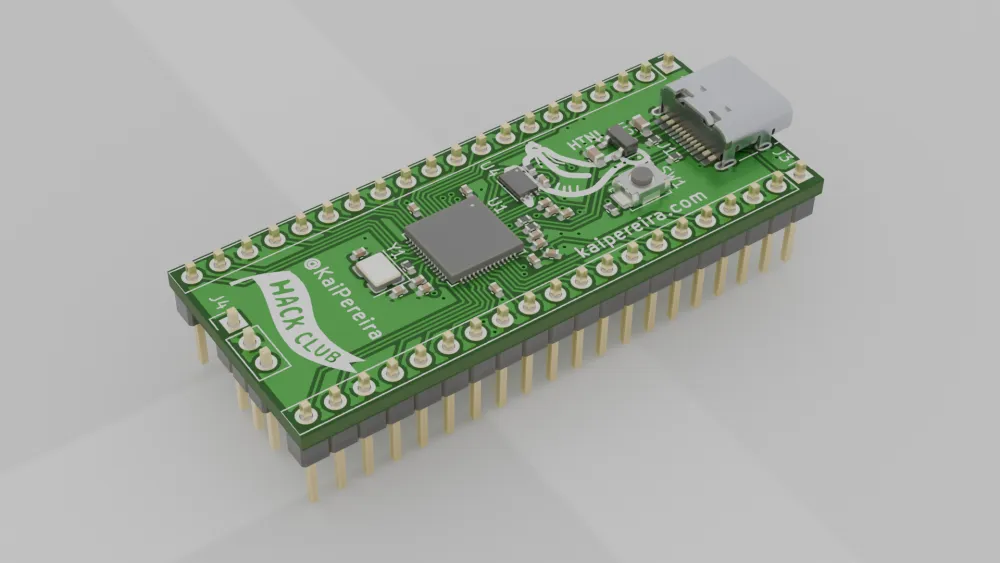
Congrats on finishing your devboard 🥳
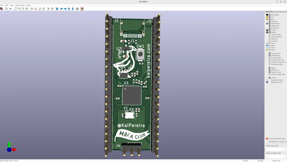
Now you've finished making your actual PCB, if you want to get an idea of how it'll look when manufactured, you can tap the 3D Viewer in the top toolbar:
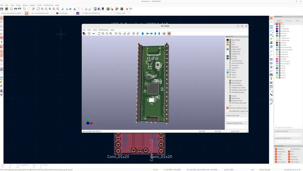
The headers will be facing the other way and you can't see the USB-C because it doesn't have a 3D model, but this is how your PCB will look! Pretty cool huh, but you know what would make it even cooler... Art!
Working on silkscreen
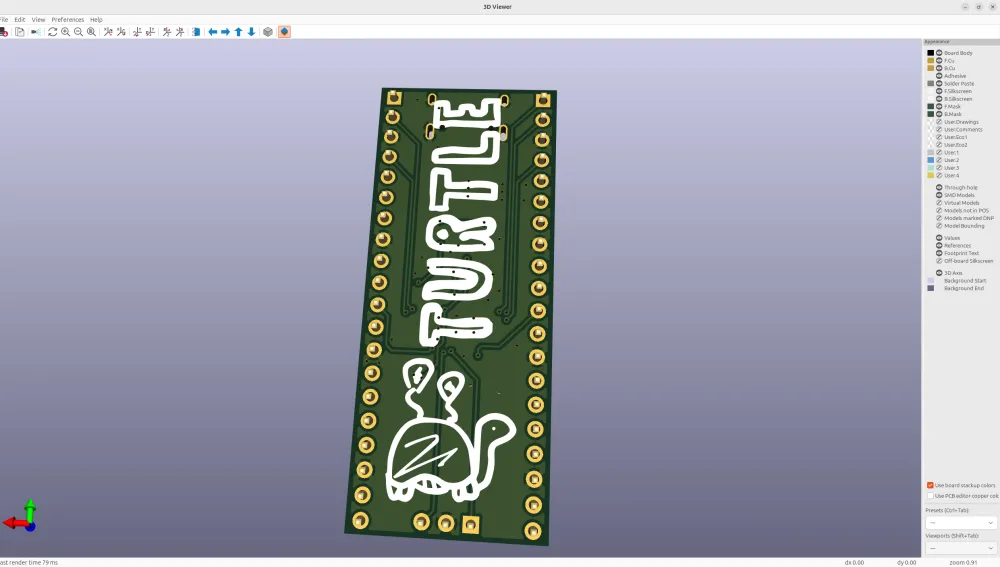
Now before we get all excited, let's polish up our PCB a little bit! We're going to do this by modifying what's called the silkscreen, this is all the white stuff you see on the PCB, it's purely decoration and used to show where components should go when soldering, and also to label stuff, and you can make art with it.
But before we get to make the art, let's move all the labels on our PCB to look nice and organized! Now the capacitors and stuff aren't too useful to us, so we can delete those silkscreen labels like "C#" or "R#", and just leave the important ones for the connect, the pi, etc.
I'd suggest hiding some layers to make it easier to see, so delete all the stuff we don't want, and organize the stuff we do want (You can also hide the fab layer for now, but there's no need to delete that stuff, it won't be on your PCB):
This is how mine looks when done:
Now, let's add our own art! Try out the KiCad image converter, and also add some text and stuff to your PCB. I personally like to add things like my website, github handle, favorite animals, anime, whatever you want really.
I personally use excalidraw to draw my art but you can do whatever:
And that's our PCB finished! Run DRC one last time to make sure you have no errors, and then continue on to the final step, which is getting this thing manufactured!
Fabrication time!
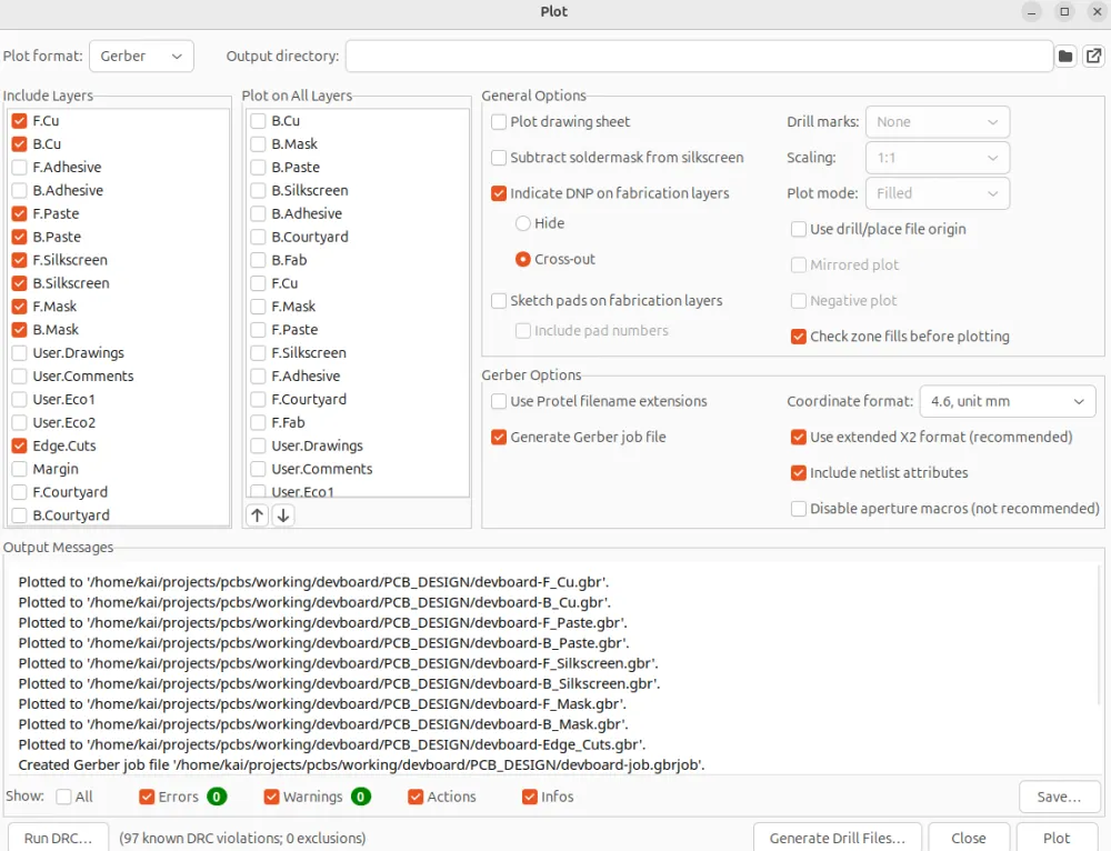
Now that we've finished our PCB, let's get it fabricated. Save your PCB, and then go to:
File -> Fabrication Outputs
and then export every single thing there, if you want my gerber settings, here they are:
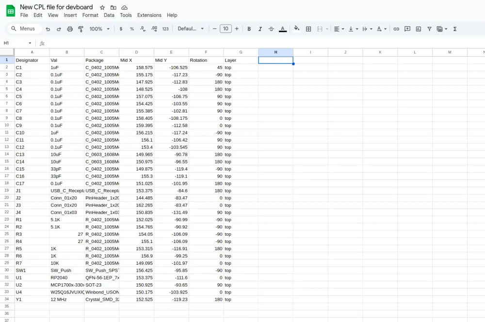
And before you turn all these files into a zip, you'll want to modify the CPL file, because JLCPCB expects the CPL file headers to be called something else, so add it into google sheets. This file will be called something like "your-project-top-pos.csv", we're doing one sided assembly so you can delete the bottom file. Anyways change the headers from:
- Ref -> Designator
- PosX -> Mid X
- PosY -> Mid Y
- Rot -> Rotation
- Side -> Layer
Next, you need to replace the headers on your BOM file, this is just changing Designation -> Comment
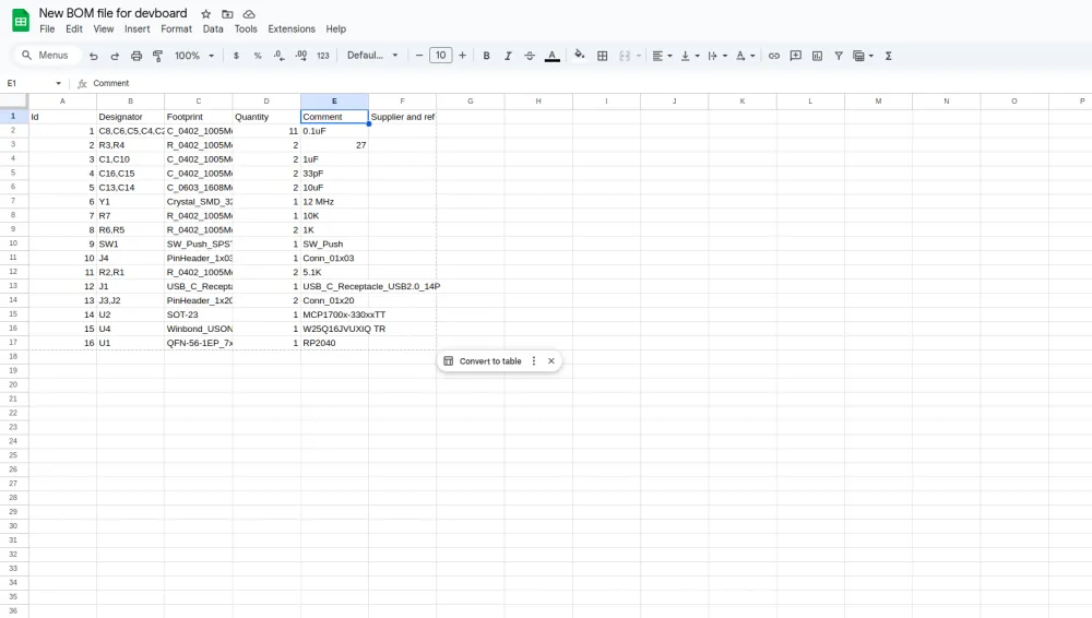
Once you've renamed those headers exactly, export is as a .csv and replace your old CPL/BOM file with this one. And then take all of the files you exported, and compress them into a zip folder, called "PRODUCTION" or whatever you want really:
And now I usually make another folder called production in my root, and put this zip file inside of there:
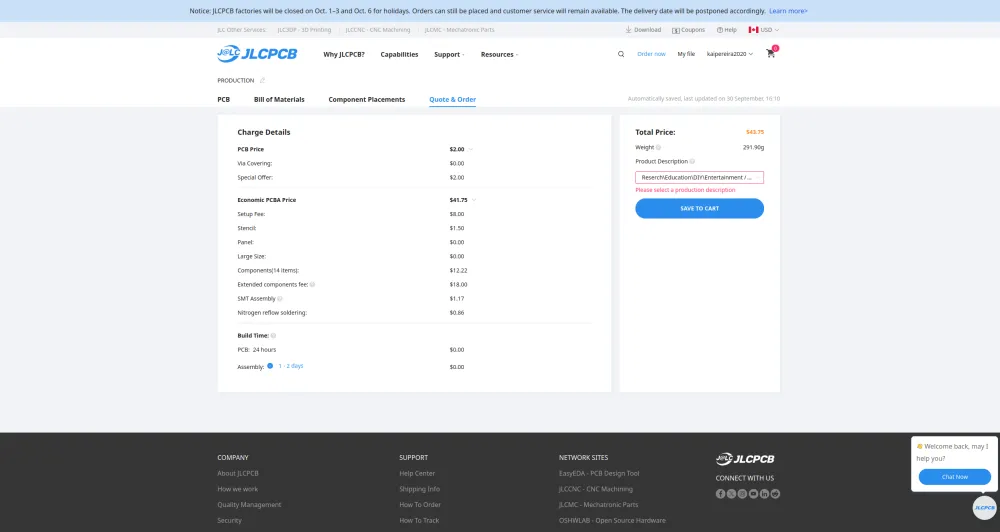
Now head on over to JLCPCB and drag that zip folder into the quote section. You should see your PCB show up, and the only thing you're going to add onto your order is PCBA, this just makes sure that JLCPCB doesn't just give you the raw PCB, but also assembles it:
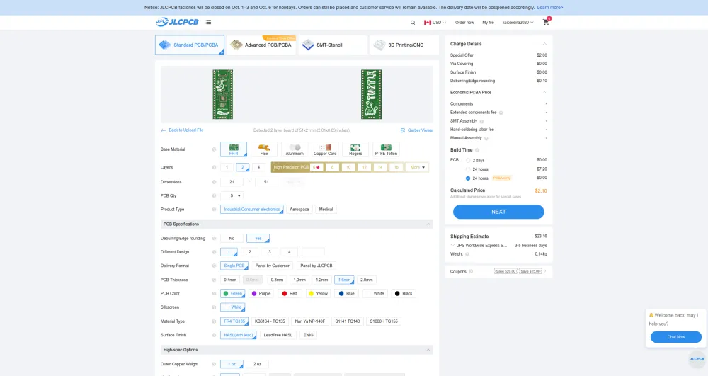
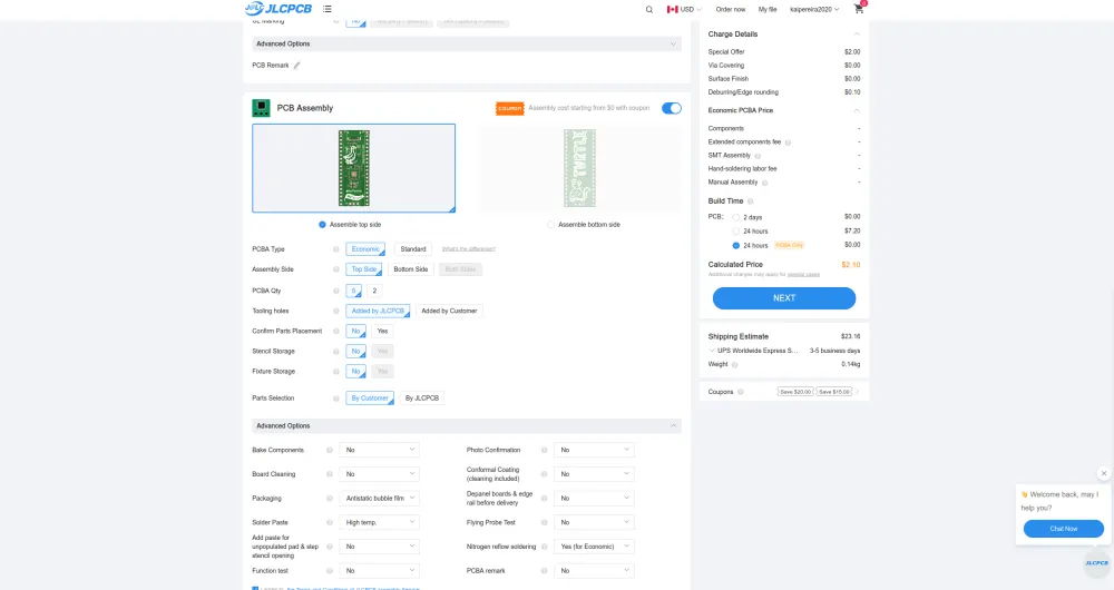
Now tap next, and then add your BOM, and the CPL CSV you just created. If you have any errors when uploading this, check the internet, double check you modified the CPL/BOM properly, and worst case, tap the chat button on the website and ask the JLCPCB help desk.
If you did everything properly though, you should be presented with the JLCPCB BOM page:
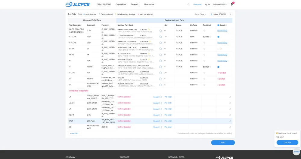
Now we need to assign the parts that JLCPCB couldn't automatically find and the ones it got wrong. In most cases this is just a quick search and then tapping the first result, but make sure what you select is exactly what you actually want. The 27 ohm termination resistor is also probably going to be wrong, so you'll want to re-assigned this to a proper 27 ohm resistor.
Make sure not to select the pin headers for PCBA, these are easy to solder our self and aren't worth it to pay for, just buy these separately.
Also make sure you're using as many basic parts as possible, filter for these so that your PCB is cheaper when selecting parts, but sometimes parts aren't available as basic
You might also have problems with the flash memory part, just use the W25Q16JVUXIQ part instead of W25Q16JVUXIQ TR (they're the same thing, just TR specifics it's in a tape roll which you don't need to worry about)!
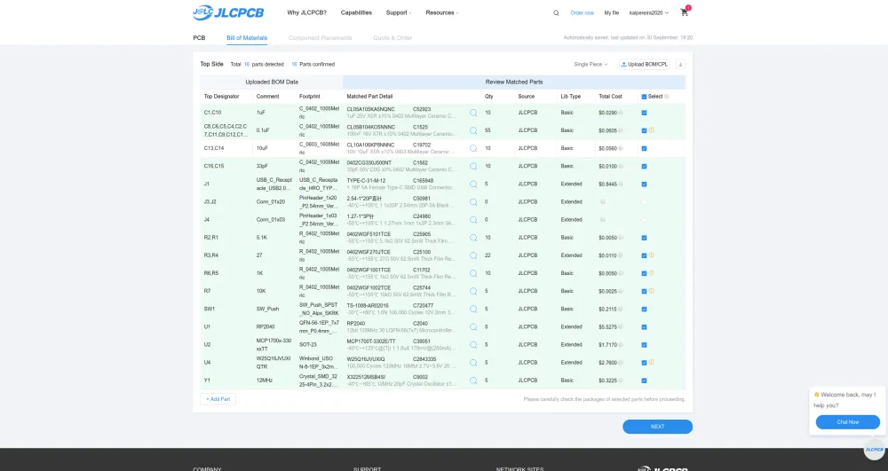
This is what my final BOM looks like, feel free to copy mine (it'll be in my GitHub repository under /PRODUCTION/files too):
Now continue on, and don't place the header pins (it'll prompt you), and then you'll see your assembled board show up:
But there's a couple components that aren't properly assembled on our boards so we need to move them manually!
You'll need to move:
- The USB-C to fit within the holes nicely
- The LDO just needs to be turned a bit
- The flash memory needs to be rotated right so that the dot aligns with the triangle
And then everything else you should just double check, but it should be fine:
Now, tap next, and congratulations, you're done your PCB!!!!
Congratulations on making your first PCB!! I know that this seemed pretty hard and complicated, but it gets so much easier with practice, so keep on making cool stuff!
Now try to challenge yourself in your next endeavor, and don't just make another devboard, try your hand at a motherboard, or a power controller, just something that challenges you and helps you learn!
Feel free to also modify this board you've created to include an LED matrix, motor drivers, literally whatever your heart desires.
I hope you learned alot, if you want to checkout some of the other stuff I've created, check out my projects on GitHub or my personal website https://kaipereira.com/!
Now if you want to stick around, we're going to go through assembling your PCB, if you didn't want to get JLC to do PCBA!
Hand-soldering your Devboard!
Now if you've decided to take the VERY FUN ROUTE of hand soldering your devboard, I'll continue with a small tutorial on how to do so!
Now hand soldering is mildly difficult, and takes quite a bit of time, but you'll learn invaluable skills lots of other people don't learn, and also earn a lot of tickets while you're at it :D
So the first step is buying all your components for hand soldering! Everything can just be bought on LCSC, and I'd suggest buying a couple extra components of each thing, just in case you accidentally mess up/break components!
You'll also want to have a couple other key components:
- Flux paste (not solder paste), this helps the solder bond to the pads of your board, helping to fix mistakes and is crucial. This will come in a little syringe container, and looks white/yellow depending on where you get it from (solder paste, which you don't want usually look gray!
- Fine tip soldering iron, this makes soldering in really tight spots so much easier, most tips are usually fine enough, but you just don't want like a super wide one.
- Solder, usually smaller solder is usually more convenient, but it's honestly fine to use larger
- Fine tip tweezers, I honestly wish mine were finer, but I'd suggest trying to find the smallest fine tip tweezers in your house that aren't ribbed/textured at the end
- Brass sponge, for cleaning your tip, you just dip your iron into this every once in a while to get the excess solder off!
- Silicon mat, this isn't needed, but I would HIGHLY suggest, so that your soldering iron doesn't fall off and burn you, and so you have a nice grippy surface to hold your PCB on
- Decently ventilated area, honestly I find this is less for saving you from the unhealthy fumes and more to get the smoke out of your eyes so you actually see what you're doing!
- Isopropyl alcohol and Q-Tips, these are to clean up the flux on your board after soldering, it's just once you're done, so you don't really have to have it on hand before starting!
This is what my setup looks like with all of these things:
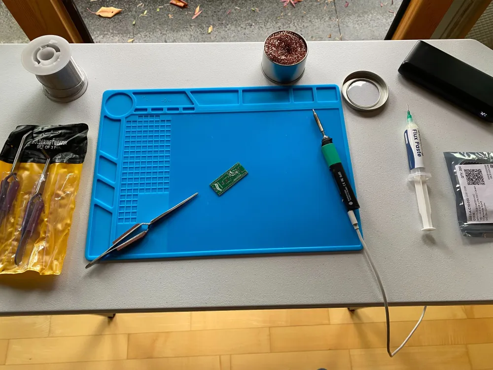
Pretty sweet right :D
Now you're ready to get soldering!
When you're soldering a small board like this, and most PCB's for that matter, you'll want to start with your smallest components first and then work your way up. In our case, we have quite a few 0402 components, which are going to be SO MUCH FUN to solder.
Lots of people don't spend time to actually learn how to properly solder these components and just go at it, but I'll try my best to describe it and you'll also want to watch this video in it's entirety!
So basically:
- Apply your flux around/in the pads of the footprint of the components you're going to solder
- Apply solder to one pad of the footprint
- Place your component onto the footprint
- Apply heat on the pad with solder while it's touching your component
- Take your tweezers off the component
- Apply heat to the other pad, and solder it to the component
- Apply more solder to the pad you first soldered to create a stronger connection
And then you're done! I sometimes add some more flux and then clean up my joints, but it's up to you if you want to do so! This will be hard when you first start off, but it get's much easier with practice, and also better tools help a lot!
Now you want to pay close attention to your joints, to make sure that your solder is actually joined with the component! I find being in a WELL lit room helps a lot to see everything, and a microscope can be very handy!
If your component didn't form a joint with one of it's pads, you might need to get the component closer to the pad or apply flux, or apply more solder!
If you ever bridge 2 pads with solder, apply flux and they should go back to their relevant pads, it's MAGICAL....
Tutorials help a LOT here where words sometimes can't explain all, so take your time, and do it right.
I started by soldering my 0.1uF caps, because there's quite a few of them, but you could really start with whatever 0402 component you want, and then work your way up to 0603, then 0805, and then small components, then large components!
Yes, it's SMALL, and takes lots of time. If you're currently working on this, shoot me a DM on slack @KaiPereira, I'd love to see how you're doing!
I haven't finished the rest of soldering my board, but it'll be added soon :D