Blinky Board
Made by @CAN
Hi there! This is a tutorial on how to make a 555 LED Chaser board otherwise known as a “Blinky Board”. You can follow this tutorial, customize your design and you will be shipped the parts to build it!
Blinky Board (Preferred)
Check out the (preferred) KiCad version here!
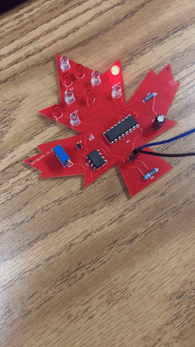
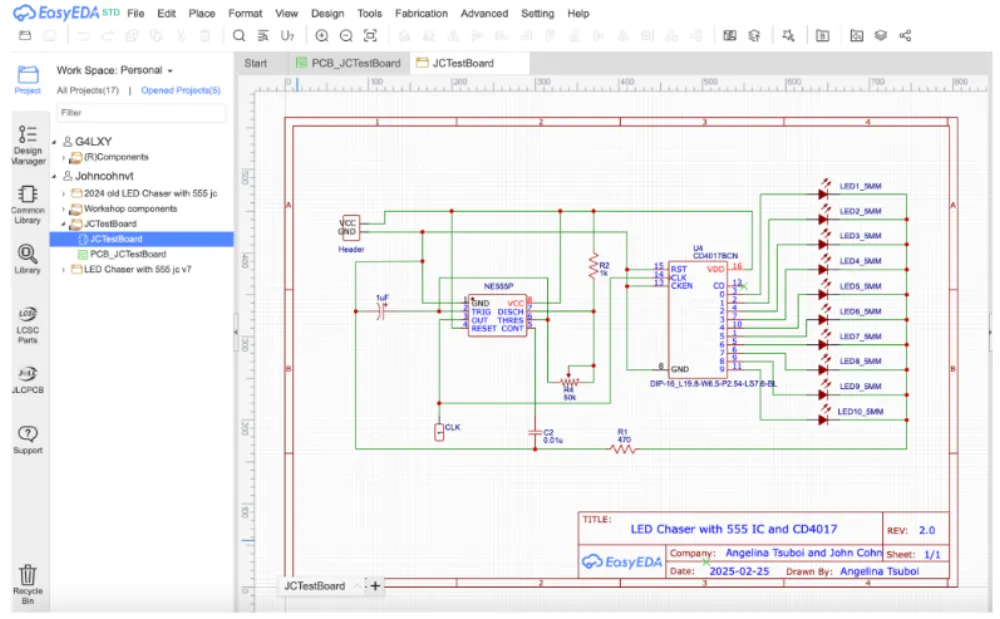
Here is what we will be building:
We will all build this LED chaser which blinks 10 LEDs in a variable speed sequence.
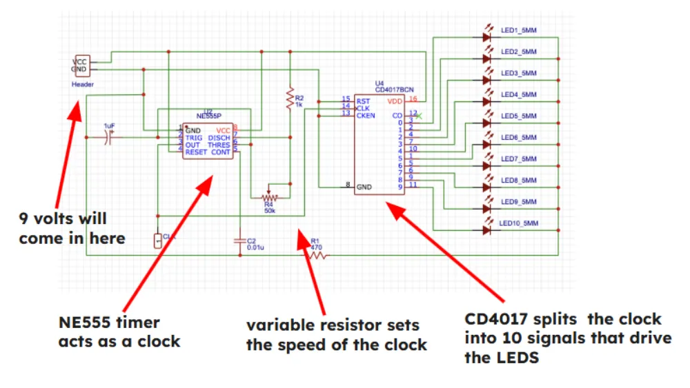
Here’s the schematic:
What we’ll be doing
- Set up EasyEDA/GitHub
- Design a Schematic
- Create a Printed Circuit Board (PCB)
- Submit your board for manufacturing at JLCPCB
- Get a PCB grant from Hack Club Blueprint
- Wait a week for your board to come back
- Solder your board
- Test your board and enjoy!
Set up accounts
If you haven’t already, you should create an account on EasyEDA and GitHub. EasyEDA is what you will use to design the PCB and GitHub is where you will share it.
Creating your GitHub Repo
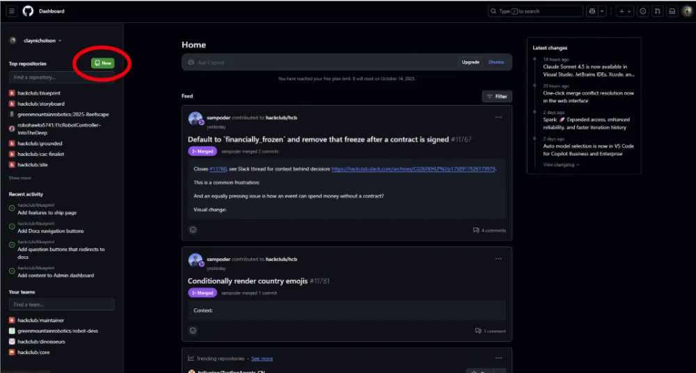
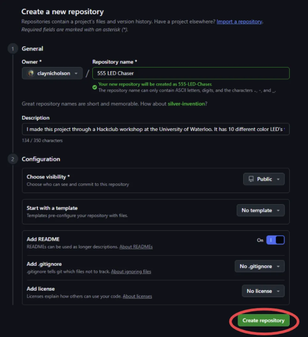
Create a repository on Github.com. (you may need to create an account)
You need to
- Name it - I named it 555 Chaser but you can do whatever
- Write a nice description - this can be short
- Make it public
- Enable a README so others can see what you made
Now copy the URL for your repo. You will need it for your next step.
Creating your project on Blueprint
Now, you just need to create your project on Blueprint. Blueprint not only allows people to share projects, but acts as a gallery of all the projects made.
First, create your Blueprint account on https://blueprint.hackclub.com/ (⇒ Sign in). In the future, you will be able to log into your account anywhere, anytime to make your project.
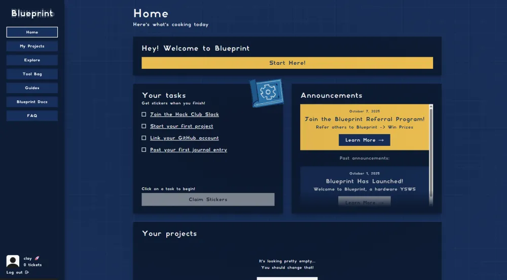
Your screen should look something like this.
Click the “+ Start a Project” button at the bottom of your screen. You need to fill out the form (you can just copy the name and description from your GitHub repo). Don’t worry about the banner for now. You can put that in later.
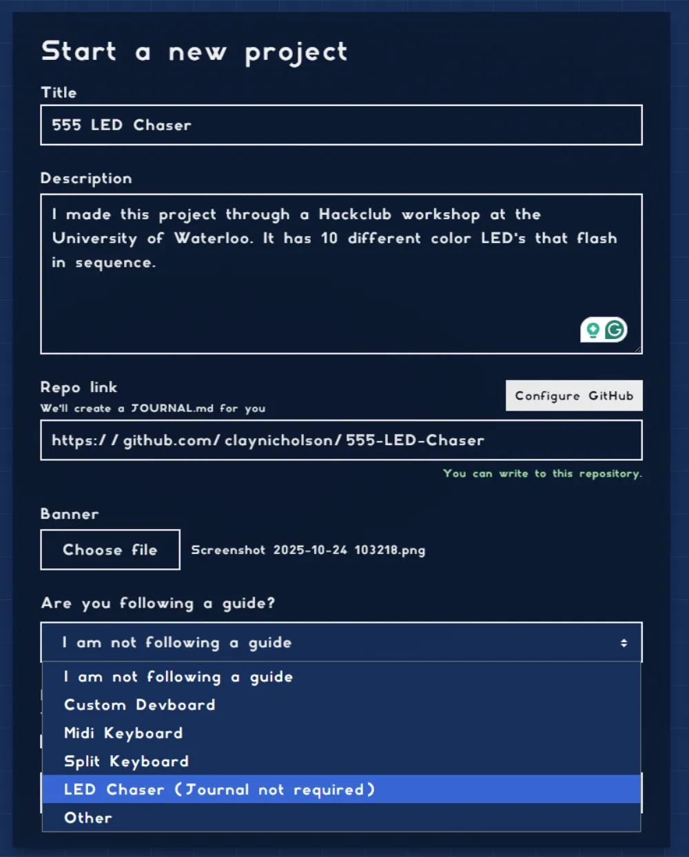
IMPORTANT:
Make sure you select the LED Chaser as your guide. Doing this will bypass the need for a journal in order to ship. For your future Blueprint projects, you will need to make an updated guide with what you are making.
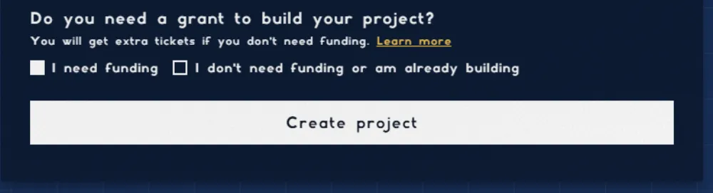
Also, make sure you click “I need funding”
Now click “Create Project”
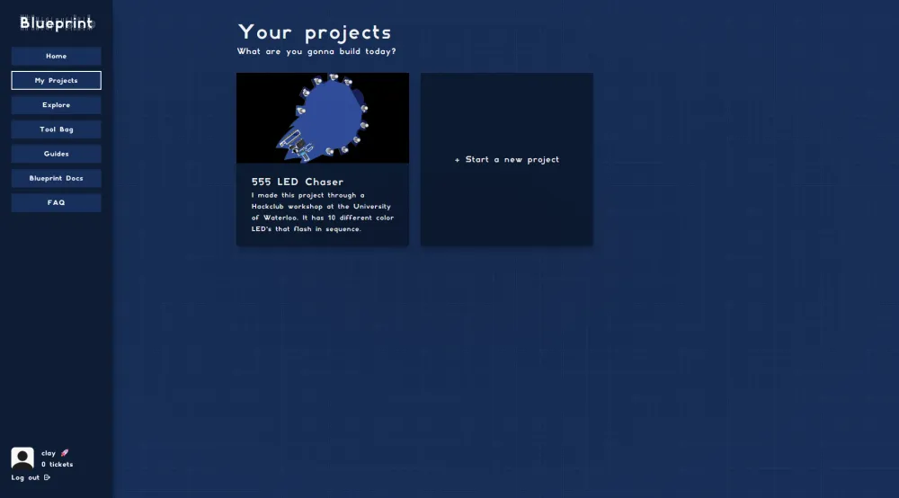
Once your project is created, click into it on the project screen.
Create your project on EasyEDA
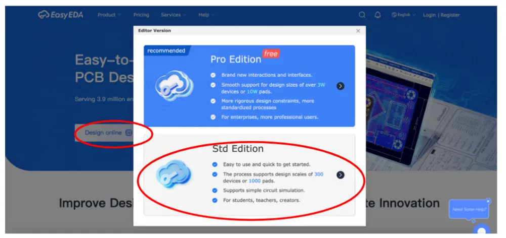
Go to easyeda.com/editor and click Design Online > STD edition. We are using the standard edition for simplicity sake but the pro edition is nice and its free!
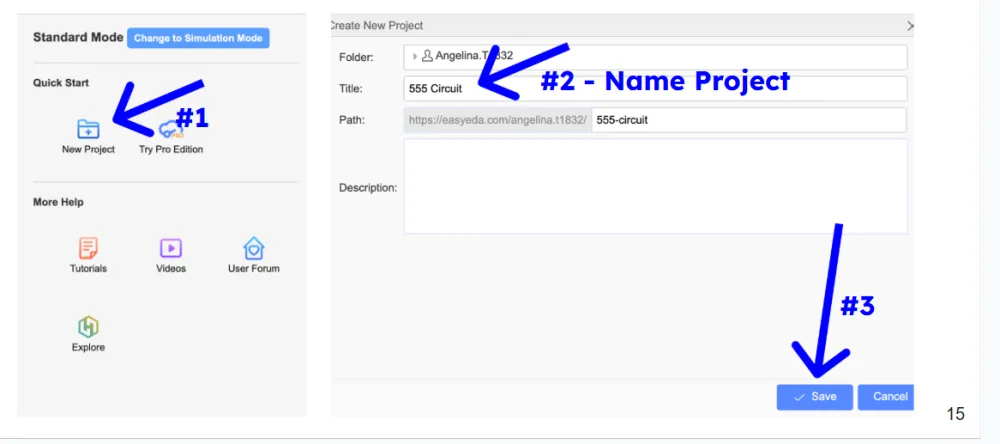
Now click New Project > Name your Project > Save
Create your schematic
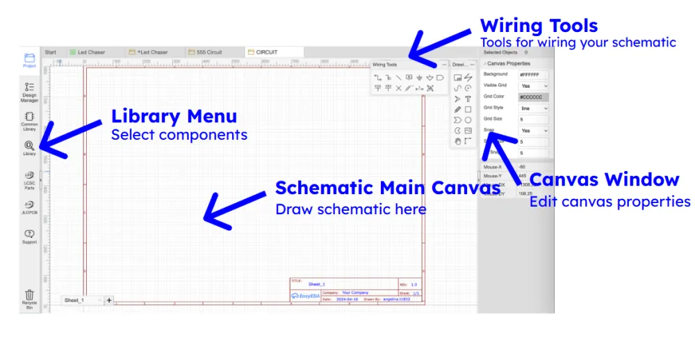
You should see something like the image below. That is the schematic editor where you will be making your circuit diagram. Below are some useful tools.
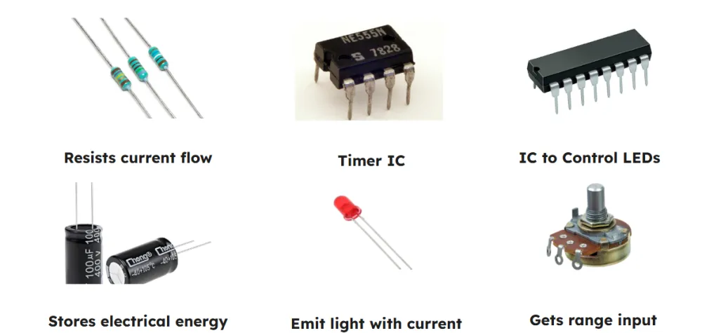
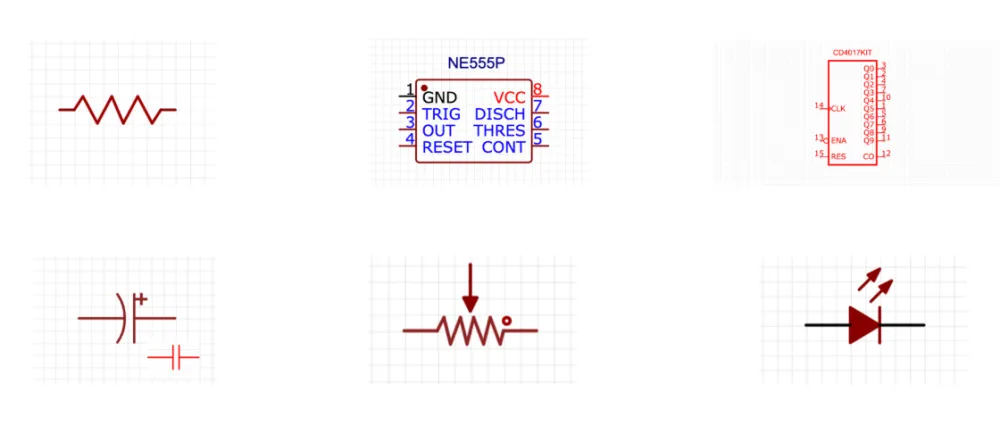
Here are the components we will be using: (IC stands for Integrated Circuit)
In schematic, things are represented as symbols. Here are the symbols for the components above:
In order to place components (aka symbols), you need to click “Library” and search for a component number such as “CD4017BCN”.
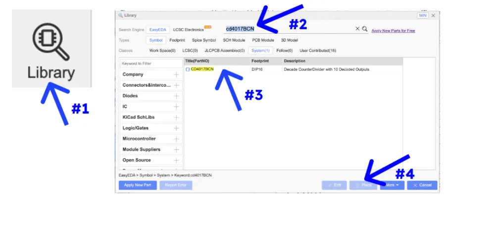
You will now need to go through and find all of your components. Luckily, we already compiled a list of everything you need to place. Go to Library>Click on the part number>Place for each of the parts below:
- C46749 (this is your 555 IC which is famous in circuitry)
- C32710674 (this is your main 4017 IC. It controls all of the LED’s flashing given an input from the 555)
- C492401 (this is your header, or little pins which you will use to power your circuit)
- C81276 (this is another little header which you can use for debugging your circuit)
- C62934 (this is an electrolytic capacitor, it is directional so be careful!)
- C249157 (this is another cap)
- C713997 (this is a 1k ohm resistor)
- C58592 (this is a 470 ohm resistor)
- C118912 (this is a potentiometer otherwise known as a variable resistor. You can use this to control the speed of the flashes)
You will also need to place a total of 10 LED below. You will get 10 of each color in the kit so don’t worry about assigning their color right now!
- C2895480 (normal LED)
In the kit, you will be given
- 10x Red LED's
- 10x Orange LED' s
- 10x Yellow LED's
- 10x Emerald LED's
- 10x Blue LED's
Here is a good point to remind you. If you ever need help, ask in #blueprint-support on the Hack Club Slack.
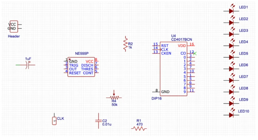
Place your components
Now that you have placed all of your components, you should arrange it as below. This will make it easier when you wire.
- You can use ‘r’ to rotate them
- Use Copy and Paste when you need more, E.g. to make 10 LED’s
- Remember to save (Control-S or ⌘-S) often !!!!
Wire your components
Don’t mess this up! Make sure your wiring matches the diagram below. The little red dots indicate that two wires are connected. Make sure that the wires which are supposed to pass over each other are not connected!
- Click “w” or the wire button, or click on a terminal of a component
- Wire together GND of all the LEDs
- Check out Shortcut keys (Settings-> Shortcut key settings)
- Remember to save (Control-S or ⌘-S) often !!!!
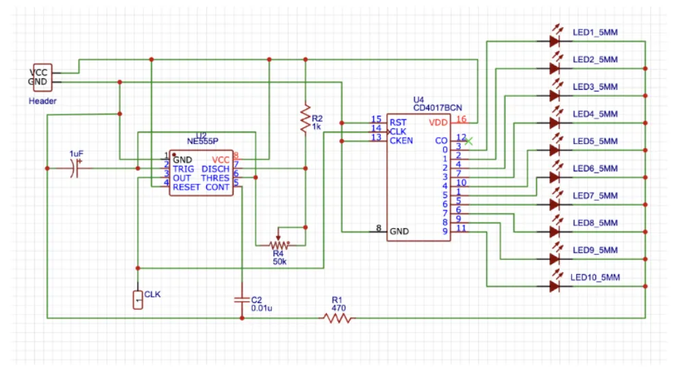
Your schematic is complete!
Reminder: ⌘+ S OR Ctrl + S to save your design often!
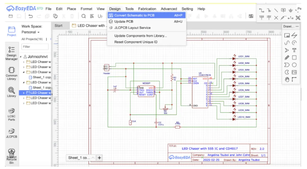
Create a Printed Circuit Board (PCB)
Now, its time to convert your schematic (circuit connection guide) into a PCB (the physical layout of the connections).
At the top of your screen, click
Design > Convert Schematic to PCB
Create an outline for your PCB
For this tutorial, I will be making a rectangular for simplicity sake. However,
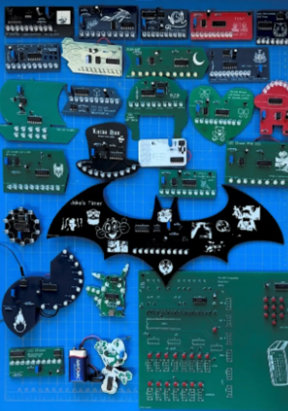
YOU NEED TO CUSTOMIZE YOUR BOARD WITH A CUSTOM OUTLINE AND ART
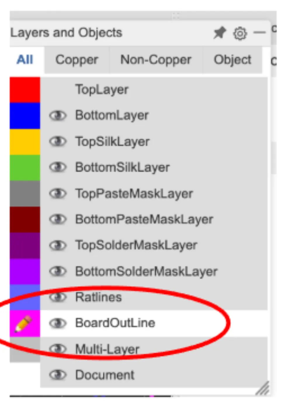
First, select the “Board Outline” on the sidebar.
Next, you can either make your own board outline using the “Line” and other features in the toolbar.
…or you can find a custom DXF online to have a custom outline.
File→Import→DXF
(you can also convert an image to a DXF using an online converter such as convertio)
One thing about the DXF’s you may need to scale it online. Make sure to always keep your board below 100x100mm.
PCB Layout
Once you have your board outline, you need to organize and wire your components. You should get familiar with the PCB tools:
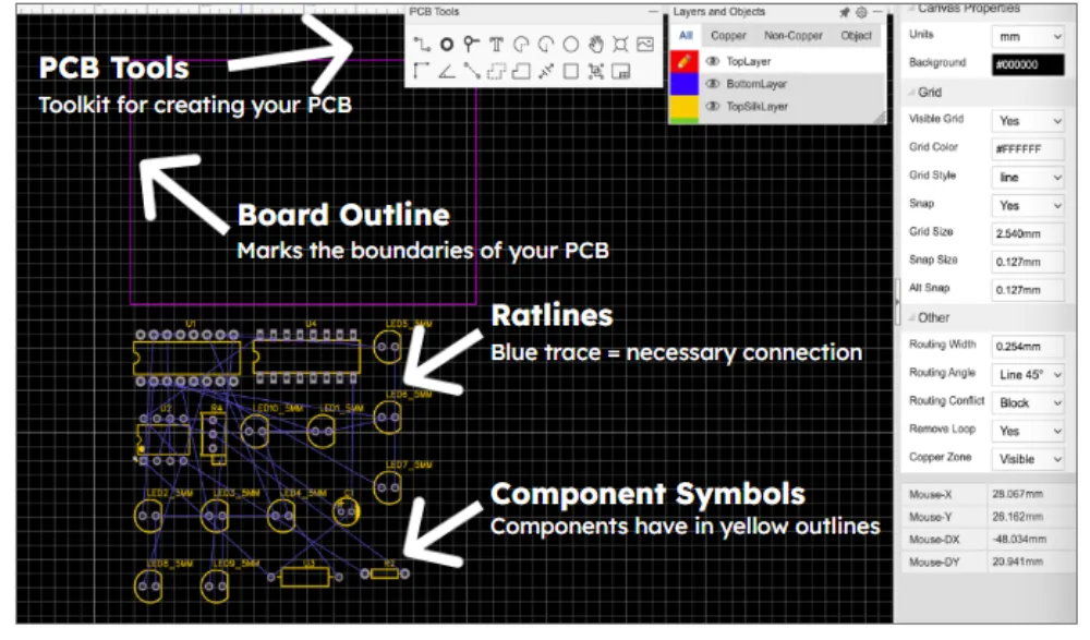
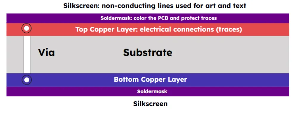
A PCB is made out of multiple layers. Our boards are “two layer” meaning that they have two layers of copper wire.
The layers include:
Top and bottom solder mask: the white ink where you can do art
Top and bottom copper layer: the layers where you make your copper wires
Substrate: The actual plastic (usually green) which makes up your board
Via: the tunnels which connect the top and bottom copper layers
Place your components
Place all of your components inside the Board Outline. Move components to shorten ratlines, which are are the straight blue lines. You can use ‘r’ to rotate.
Remember to save (Control-S or ⌘-S) often !!!!
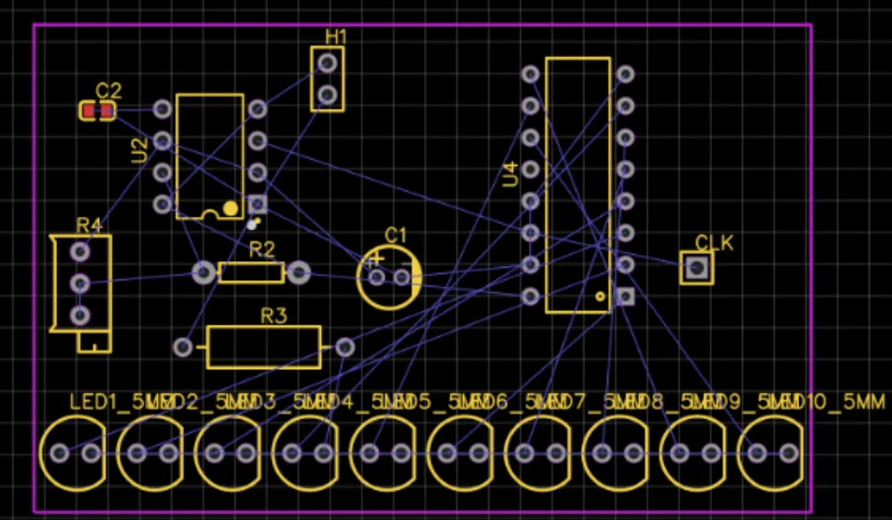
(remember that your board outline, the purple lines, should not be a rectangle but some custom shape)
Wiring your components
The ratlines (the blue straight lines) in-between your components is not the complete wiring. They are just telling you where connections should happen.
On the side bar, you can choose either top layer (red) or bottom layer (blue), or a combination of both to wire your components.
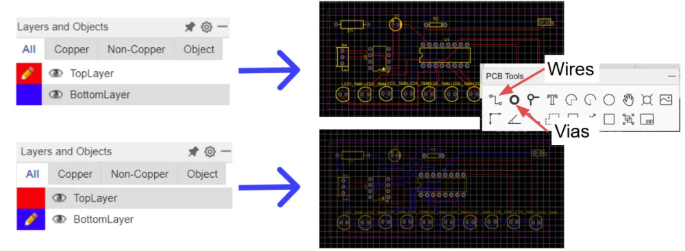
If it is impossible to make a connection in one layer, you can add a via. A via acts as a tunnel to connect between the two copper layers. As you are wiring you can click ‘v’ to place a via and switch to the other side.
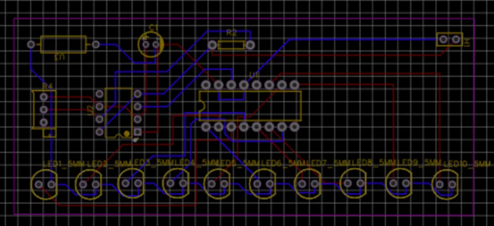
Your PCB is routed!
Customization
You may have already added some text and art to customize your board. if not, you can click “TopSilkLayer” and use the text tool.
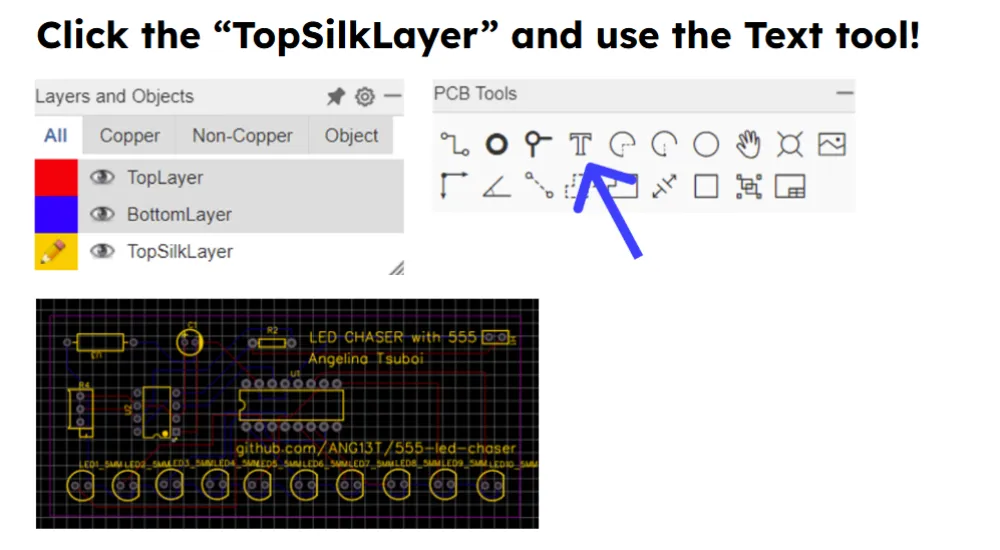
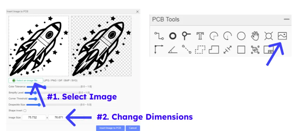
To add art, just select the “Top Silkscreen Layer” or “Bottom Silkscreen Layer” in the sidebars. Then you can do:
File→import→image
to add custom art.
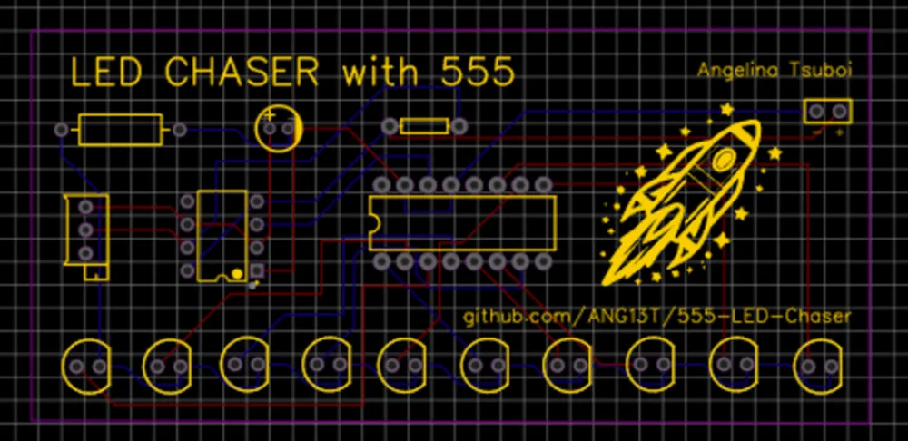
Your board is now beautiful
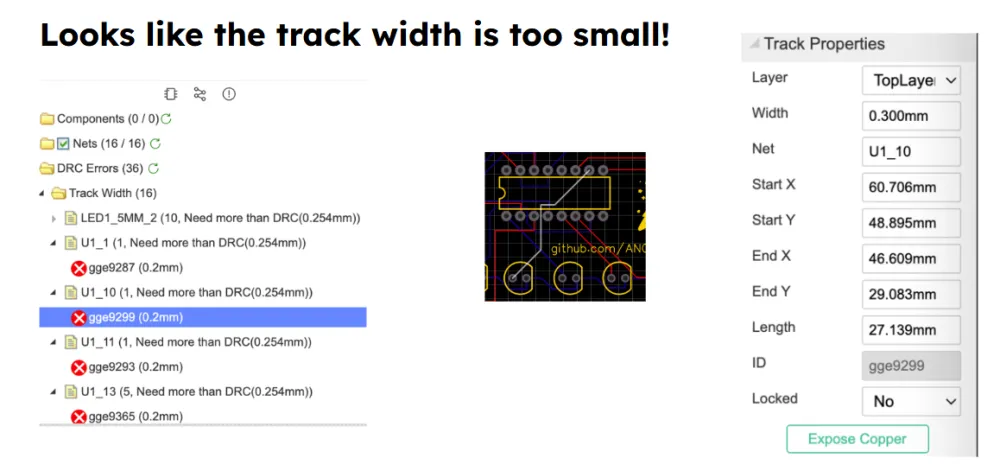
Run Design Rules Check
Click Design → Run Design Rules Check
This runs a script which makes sure that your board has no interference errors, no components are off the board, and no wires are intersecting. It does not however confirm that your board works.
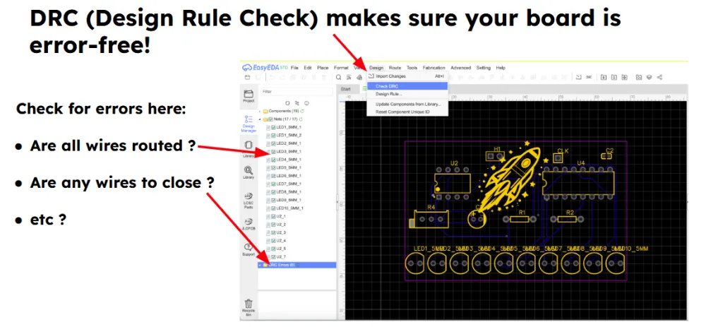
Using the output, correct any errors.
Once your PCB passes the DRC, it is finished!
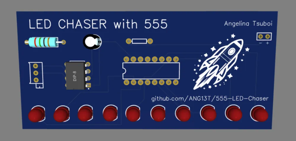
In PCB editor click View > 3D View to see your finished work!
Add your files to your GitHub Repo
Now it is time to order your board.
Get the following files of your project:
- A screenshot of your 3d view (see above)
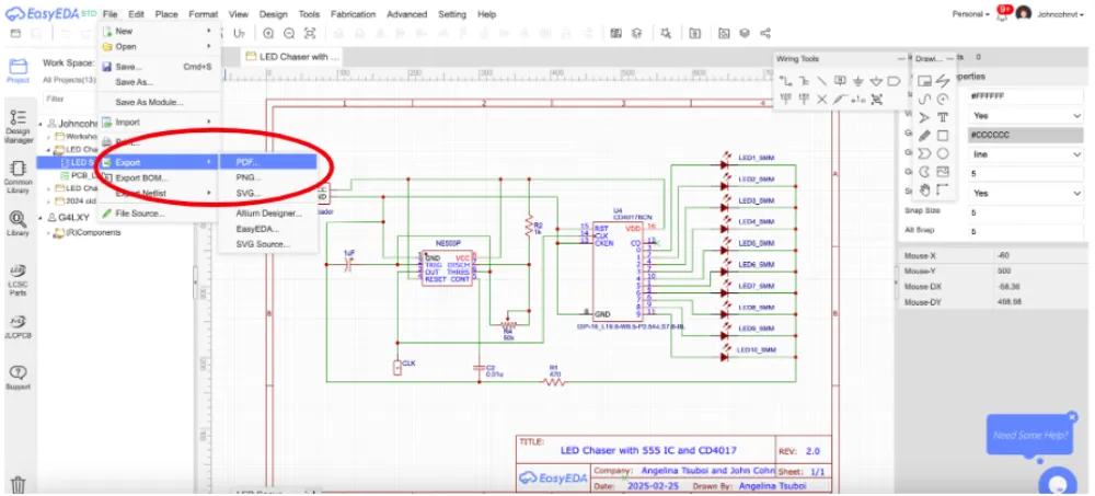
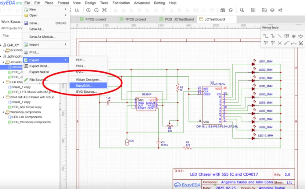
- A PDF of your schematic (In your schematic editor do File → Export → PDF)
- Your schematic (in your schematic editor do File → Export → EasyEDA)
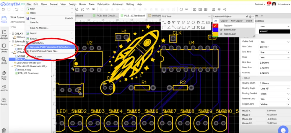
- Your Gerber (in your PCB editor do File → Generate PCB Fabrication File (Gerber))
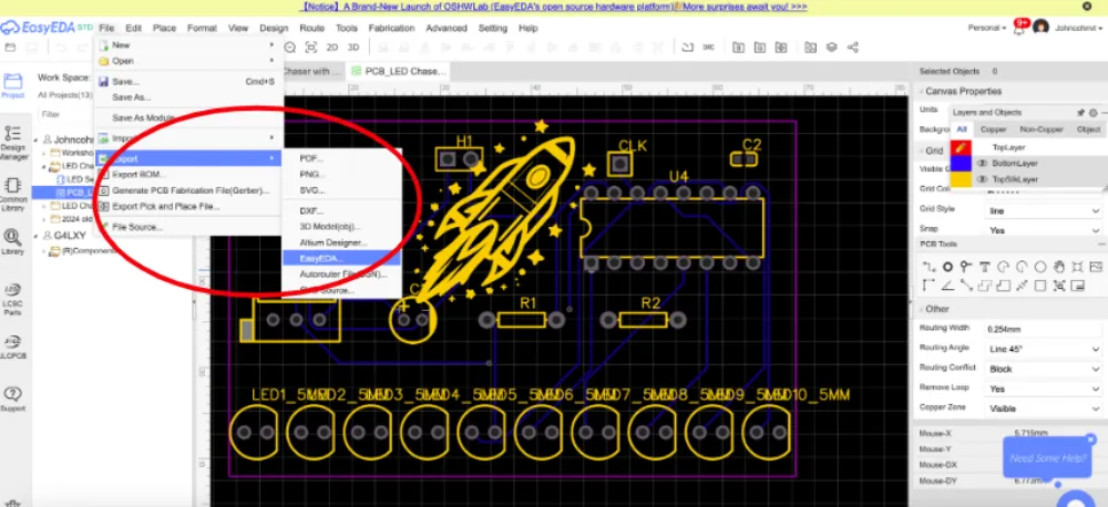
- Your PCB (in your PCB editor do File → Export → EasyEDA)
A PDF of your schematic (In your schematic editor do File → Export → PDF)
Your schematic (in your schematic editor do File → Export → EasyEDA)
Your Gerber (in your PCB editor do File → Generate PCB Fabrication File (Gerber))
Your PCB (in your PCB editor do File → Export → EasyEDA)
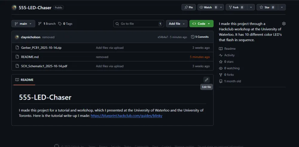
Upload your files to GitHub
Go back to the GitHub repo you created at the start.
Click Add File → Upload files
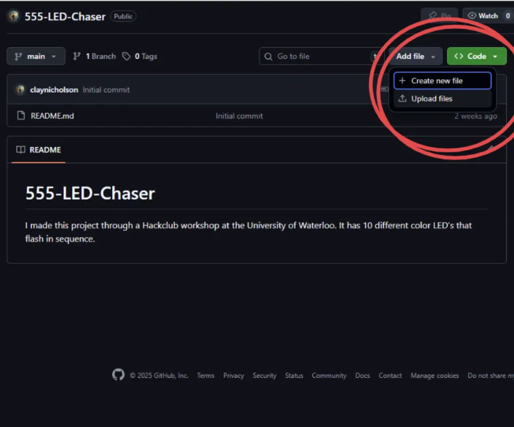
Drag in your:
- PCB Screenshot
- Schematic PDF
- Gerber
- PCB EasyEDA file
- Schematic EasyEDA file
(you should have downloaded all of these before)
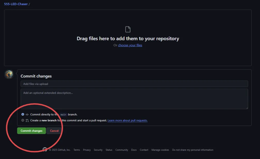
You can then click to commit your changes.
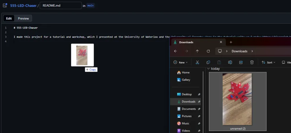
Finally, edit your ReadME
Drag in your PCB screenshot (this should be the same screenshot).
Commit this change as well.
NOTE: ALL projects you make for Blueprint must have a project photo in your ReadME.
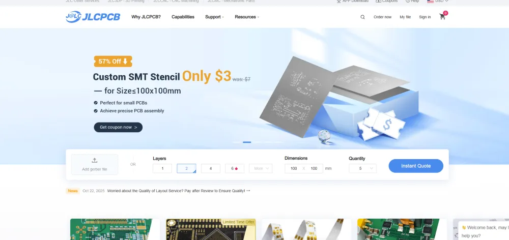
Getting a JLCPCB Price
Go to https://jlcpcb.com/ and make an account. Then, add your Gerber file for the instant quote.
Settings:
You should keep the default settings for everything. The only thing you should/can change is the PCB Color. I did black as seen below:
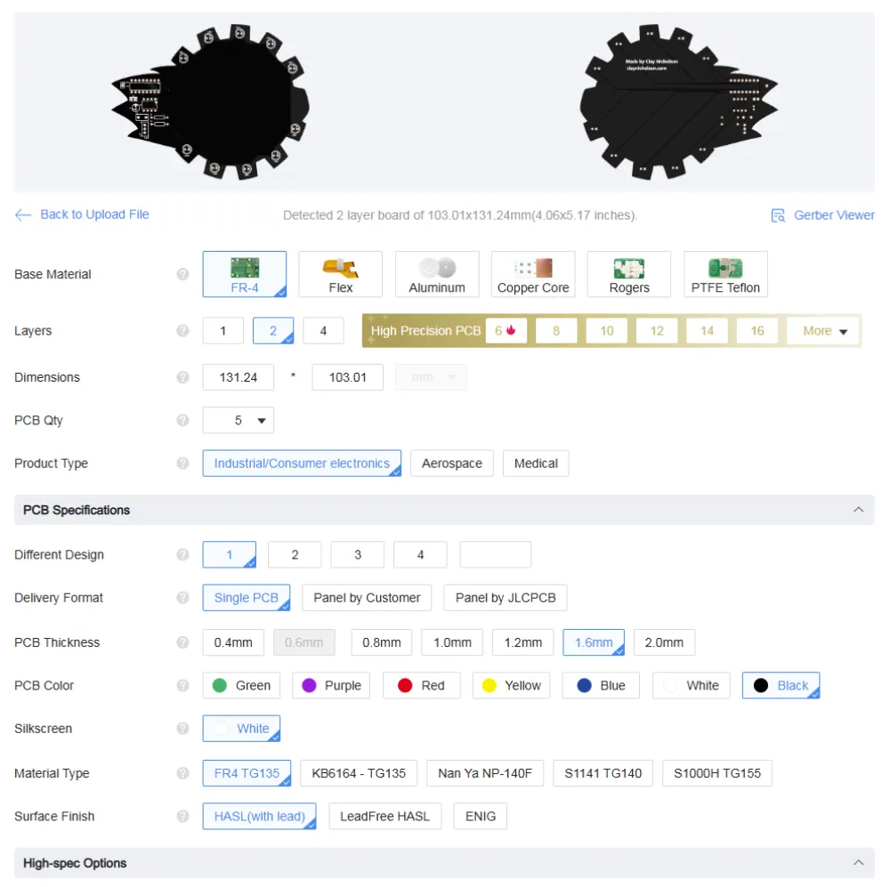
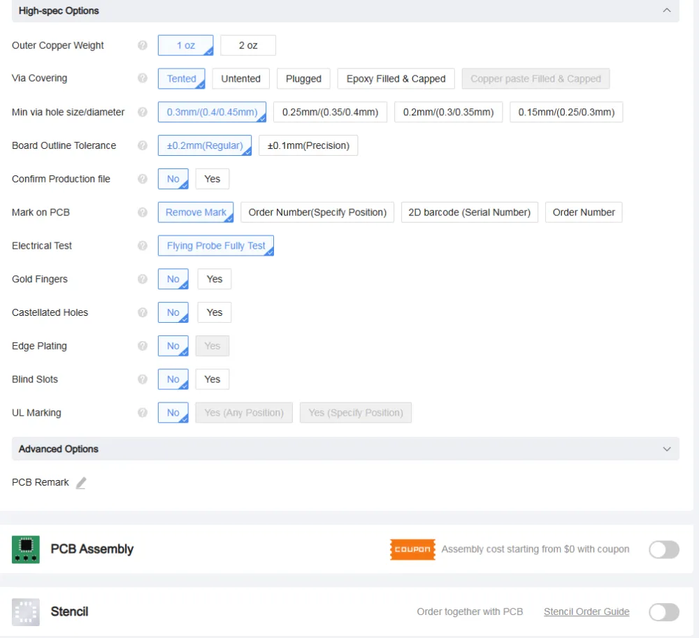
For high-spec options, also keep the default. Do not click PCB assembly as we will give you a kit to hand-solder your board.
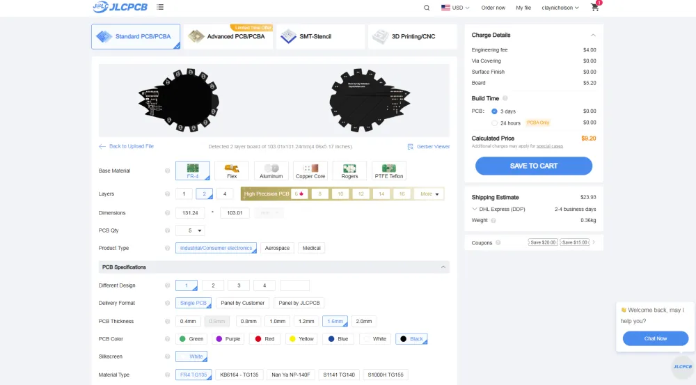
Once you have successfully Not changed any of the settings (except the board color), on the right, change the shipping method to Global Standard Direct (or Air Registered Mail if it is cheaper), and take a screenshot (this is very important).
Submitting your Blueprint project to get funding
You are almost done! At this stage you should have:
- A completed board
- A GitHub repo for your board
- A Blueprint project for your board
- A price estimate and screenshot for your board
Go back to your Blueprint project screen from before. You should edit the project so the banner is your 3D render.
Now, click “Ship It”
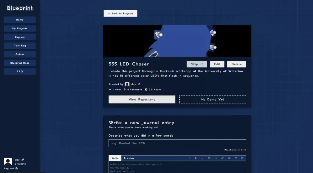
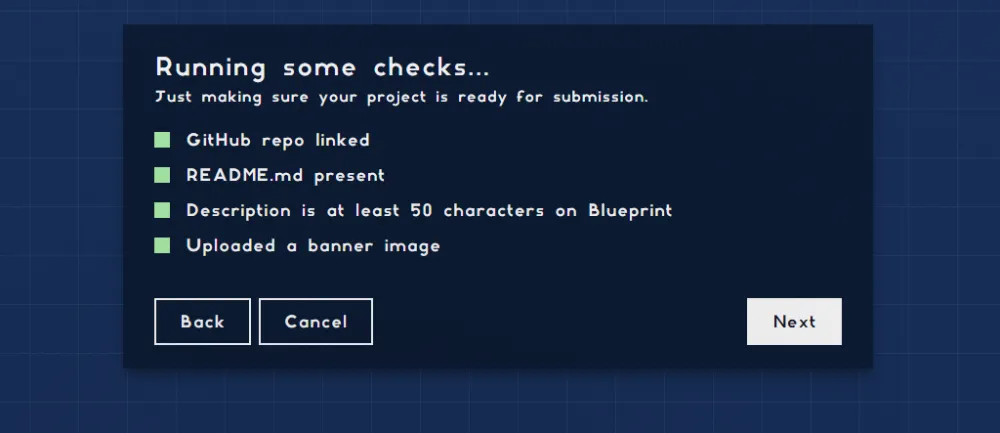
Blueprint will run some checks. If any are red, you need to fix them. (you may need to upload your project banner)
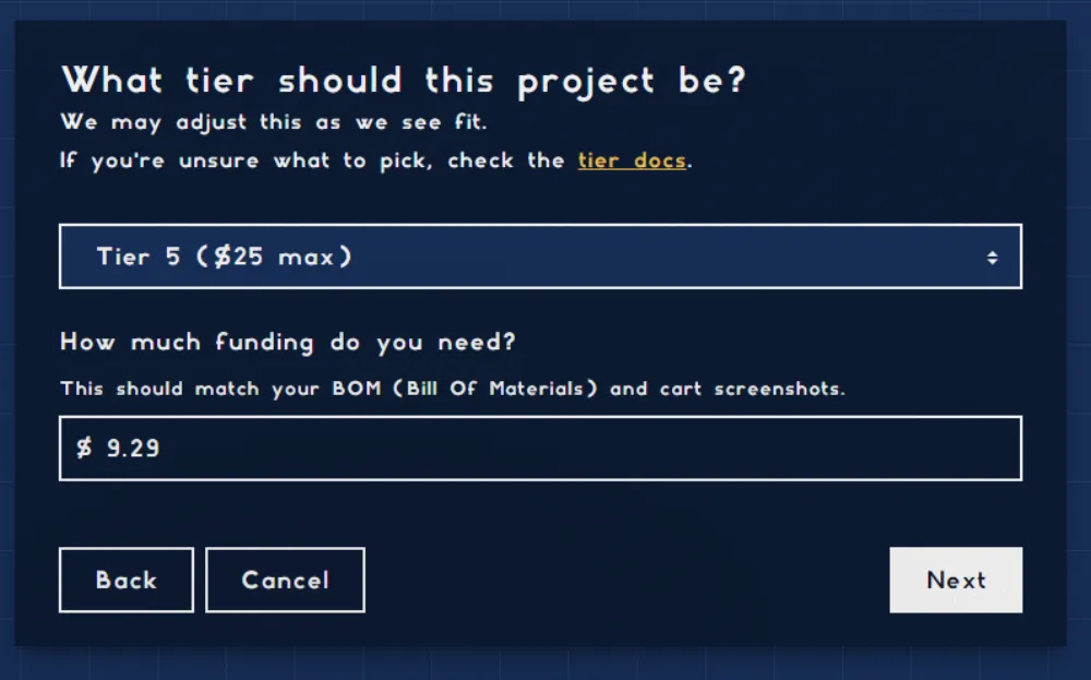
Enter the dollar amount which you previously screenshotted on JPCLCB (don’t worry, we will give you extra for any fluctuations).
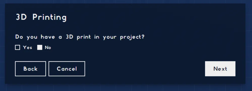
Click “No” for 3d print
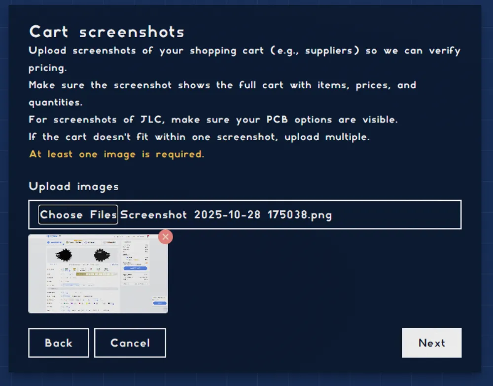
Upload your JLCPCB screenshot from earlier
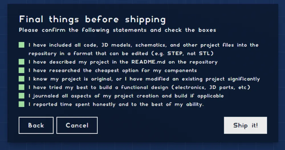
Check your project…. and ship!
You may need to verify your Hack Club identity if you have not already.
You are done!
You should wait for a reviewer to approve your project! Once it is approved, you can complete the checkout on JLCPCB (making sure to use Global Standard Direct (or Air Registered Mail if it is cheaper), and your kit/soldering iron will be sent to you!
While you wait….
Check out more Blueprint projects on https://blueprint.hackclub.com/explore! You can also make any hardware project you want on Blueprint, and get up to $400 to make it. For future Blueprint projects, you will need to make a journal throughout your development process. Again, if you have any questions, ask in #blueprint-suppport on Slack.