How to make a flight controller (from scratch)
Made by @NotARoomba
This is an advanced project. I recommend learning the basics of KiCad by making a small dev board or breadboard first. That said, anyone can follow along, as I'll go in-depth on how to build a flight controller.
I'm @NotARoomba and I have a (sort of) obsession with making flight controllers so heres a guide so that you too have the knowledge of making something cool. The files for this guide can be found here
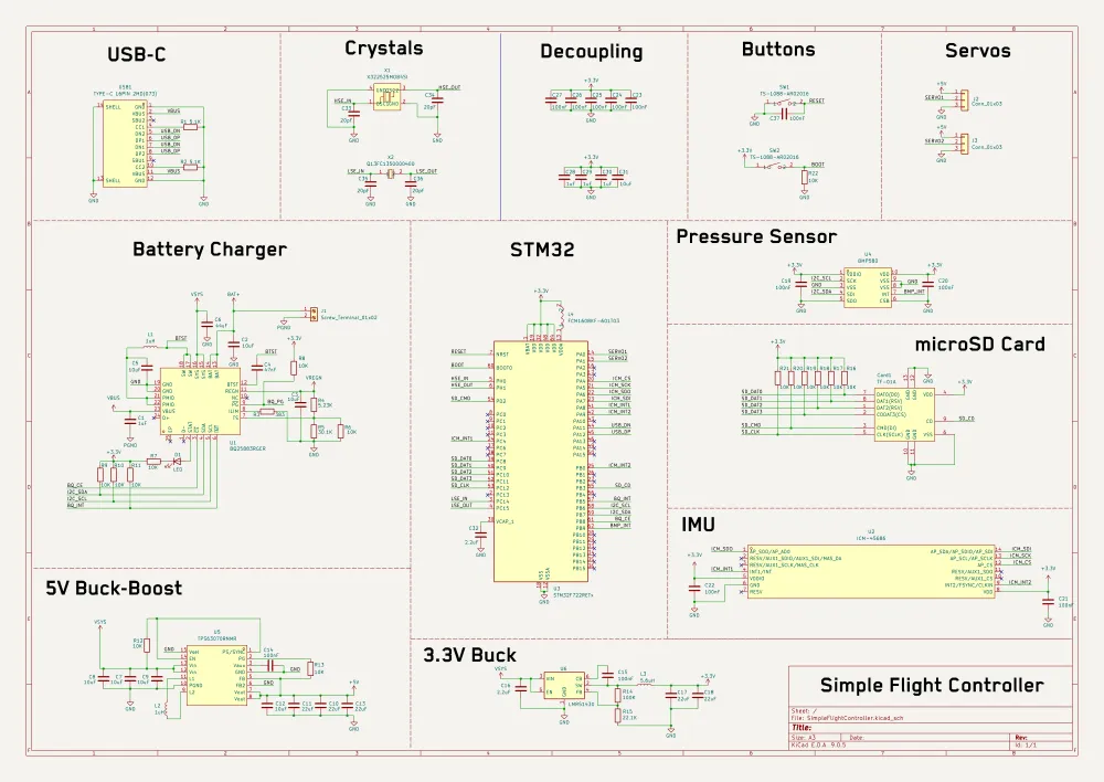
First, define what type of flight controller you want: for a rocket or a drone? Keep that in mind when starting your own design. In this guide, we'll build a flight controller specifically for rockets.
To start, create a new repository on GitHub and add two folders: hardware and software. These folders will hold most of the project files. Then, create a new KiCad project inside the hardware folder.
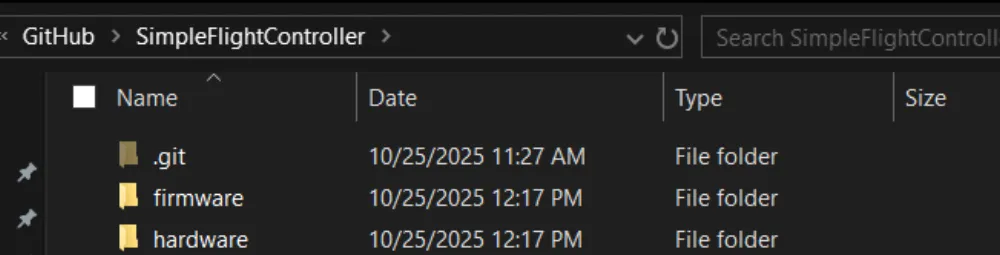
(Folder structure)
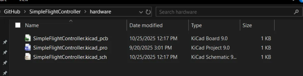
(KiCad project files)
Feature Definition
Before starting any engineering project, define the problem you're solving and the constraints you have. Imagine you want to build a rocket. All flight controllers include a microcontroller, which is a small computer that can be programmed to do various tasks. To control the rocket's flight, you'll use servos to move fins or a TVC system (Thrust Vector Control- tilting the engine nozzle to steer the rocket).
If you only build a board to drive servos, the rocket won't know which way it's pointing or how to correct its trajectory. You also need position and motion data (rotation and acceleration), plus altitude data. Finally, you'll want to store data persistently (even when powered off) for debugging and post-flight analysis.
Now that we have the rocket's functionality defined, we also need a way to power it. We can use a battery that can power both the rocket's computer and its servos.
Putting this together, we want these features in our rocket's flight controller:
- Can control servos for fins or TVC
- Can obtain position and altitude data
- Can store data even when powered off
- Can be powered by a battery
Next steps
Now that we have our requirements, let's see how to meet them. Some requirements depend on others. For example, we want battery power - but how large should the battery be? That depends on the voltages and current the servos and microcontroller need, so let's define those first.
Depending on the size of your rocket, current needs will vary because larger servos draw more current. Most hobby servos run on 5–6V and draw ~1A. A 2-cell LiPo (Lithium Polymer) battery (7.4V nominal) is common in RC applications (each cell is ~3.7V) and can be regulated down to 5V for servos.
Most microcontrollers and sensors run on 3.3V, so with a 2-cell (7.4V) LiPo we have more than enough input voltage—as long as we regulate it down to a clean 3.3V line.
Now, after checking off one of the features, we need to tackle the three others.
- Can control servos for fins or TVC
- Can obtain position/altitude data
- Can store data even when powered off
Can be powered by a battery
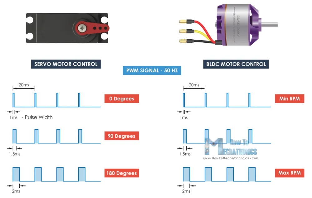
After choosing servos, we need to know how to control them. Most hobby servos use PWM (Pulse Width Modulation)—a method of control where the microcontroller sends rapid on/off pulses, and the pulse width (duration) determines the servo's position.
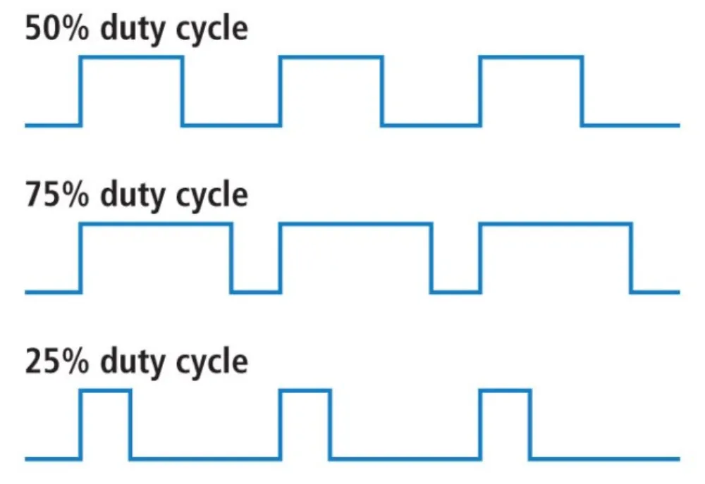
The duty cycle is the percentage of the period that the signal is high (on).
What about the sensors and microcontroller?
Needs to be able to control servos for fins or TVC- Needs a way to get position/altitude data
- Needs to store data even when the rocket is off
Needs to be able to be powered by a battery
For position and motion data, we use an IMU—an Inertial Measurement Unit. The IMU measures acceleration and rotation (and some devices also estimate altitude). We'll use the ICM-45686. While there are many IMUs with different features, this one is robust and well-supported.
For altitude, we'll use a dedicated sensor called a barometer. It measures air pressure and uses that to estimate altitude. We'll use the BMP580—a versatile and common choice for flight controllers.
Finally, to store data, we'll use a microSD card. While you can use onboard flash, microSD is more versatile when you want to access flight logs directly from a computer.
Now that we've defined the sensors and peripherals, we need to select a microcontroller. In this tutorial, we'll use an STM32, but you can adapt it to another MCU like the ESP32 if you want Bluetooth/Wi-Fi support. I prefer STM32 because it's relatively easy to program and widely used in flight controllers. After reviewing STM32 options, we'll use the STM32F722RET6 for its high clock speed and lots of peripherals. Feel free to choose another package or part for larger designs.
Needs to be able to control servos for fins or TVCNeeds a way to get position/altitude dataNeeds to store data even when the rocket is offNeeds to be able to be powered by a battery
Power Management
We have two power sources: USB-C from your computer (5V) and a battery (about 7–8.4V for a 2-cell LiPo). You cannot just wire them together. They need circuitry to choose which one feeds the board and to set the right voltages. The microcontroller typically runs at 3.3V, so we must lower the voltage (from the battery or USB-C) before it reaches the MCU.
To change the voltages, we need to use a regulator. There are two common kinds of regulators you'll hear about:
LDO—Low Dropout regulator. It only turns higher voltage into a slightly lower one. Easy and quiet, but it wastes the excess as heat.Switching regulator—A more efficient regulator. It can:buck(turn higher voltage down),boost(push lower voltage up), orbuck-boost(keep the output steady even if the input goes above or below it).
What we'll do on this board:
- Make a 3.3V line (for the MCU and sensors) using a buck regulator.
- Make a 5V line (for servos or accessories) using a buck-boost regulator so it stays at 5V even as the battery voltage fluctuates.
- Get a battery charging IC (Integrated Circuit—a chip) that can charge a 2-cell battery from 5V.
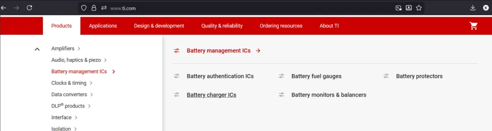
Now that we've specified what functionality we need, we need to select the chips that provide it. I personally love to use ICs from Texas Instruments as they have good documentation and a huge selection of power management chips for everything related to USB.
Go to their website (https://www.ti.com/), select "Products", then "Battery Management ICs", and finally "Battery Charging ICs". Here you can find all sorts of battery charging chips to fit your requirements for future projects.
After looking around a bit, I found the BQ25883. It's a 2-cell Li-Ion/LiPo charger (which meets our requirement). You could add a more complicated battery charger if you want more cells/power, but they take up more space and are more complex to route.
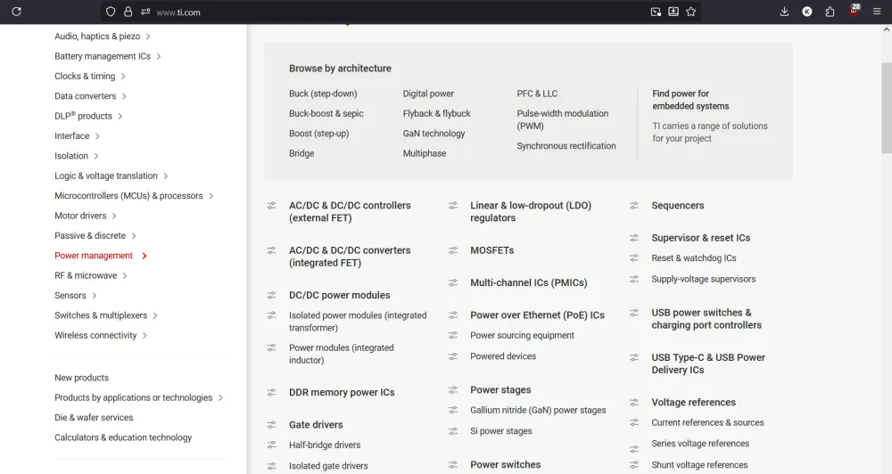
For the regulators, go back to the TI main page, then navigate to "Power Management," then "DC/DC Power Modules." Here you can find all the regulators you would ever need, complete with excellent datasheets.
Here is where we can choose the right regulators for our needs. For this tutorial, we are going to use the TPS63070, which supports 2–16V input and can output a steady 5V with high current for the servos.
Now all that's missing is to find another regulator for 3.3V. For this, we are going to use the LMR51430 as it supplies a lot of amperage for the various sensors that we will be using.
Now that we have the chips that we are going to use, we also need to verify that they are available on some platform like LCSC or wherever else you are going to manufacture your PCB. We also might have to import certain components from LCSC into KiCad.
Final component list
- USB-C
- MicroSD
- TPS63070
- LMR51430
- BQ25883
- STM32F722RETx
- ICM-45686
- BMP580
- Optional LED
Starting the Schematic
Now that we have the components that we are going to use, let's start importing them into our project.
Although KiCad has a large selection of components, it is still a bit outdated and there are tons of chips that we would have to import in order to use them. Thankfully, there is a library called easyeda2kicad.py that can import these components from LCSC for us.
I have made a simple helper script to import all of the LCSC IDs from a text file, so all you have to do is append the part numbers and run the script again.
Adding Custom Parts
Start by creating a folder called lib in the /hardware directory.
Then in the /hardware directory, create a new file called lcsc.txt and leave it empty for now.
Then create a file called lcsc.py (or whatever name you want) and paste this code in there:
import argparse
import os
import shutil
import subprocess
import sys

def run_easyeda2kicad_from_file(input_file, output_dir="./lib/lcsc", python_exec="python"):
    input_file = os.path.expanduser(input_file)
    output_dir = os.path.expanduser(output_dir)
    python_exec = python_exec or "python"

    if not os.path.isfile(input_file):
        print(f"Error: File not found: {input_file}")
        return 2

    # If a simple name was provided, check PATH; if an absolute path, check that file exists.
    found = shutil.which(python_exec) if os.path.basename(python_exec) == python_exec else os.path.exists(python_exec)
    if not found:
        print(f"Warning: Python executable '{python_exec}' not found in PATH or as given path. Trying anyway.")

    os.makedirs(output_dir, exist_ok=True)

    with open(input_file, "r", encoding="utf-8") as f:
        # ignore blank lines and comments
        lines = [line.strip() for line in f if line.strip() and not line.lstrip().startswith("#")]

    if not lines:
        print("No LCSC IDs found in input file.")
        return 0

    for idx, lcsc_id in enumerate(lines, start=1):
        cmd = [
            python_exec,
            "-m", "easyeda2kicad",
            "--full",
            f"--lcsc_id={lcsc_id}",
            f"--output={output_dir}",
        ]
        print(f"[{idx}/{len(lines)}] Running: {' '.join(cmd)}")
        try:
            subprocess.run(cmd, check=True)
        except subprocess.CalledProcessError as e:
            print(f"❌ Error processing {lcsc_id}: {e}")
        except FileNotFoundError as e:
            print(f"❌ Executable not found: {e}")
            return 3

    print("✅ All commands completed.")
    return 0

def main(argv=None):
    parser = argparse.ArgumentParser(description="Run easyeda2kicad for a list of LCSC IDs.")
    parser.add_argument("input_file", nargs="?", default="./hardware/lcsc.txt", help="Path to file with one LCSC ID per line")
    parser.add_argument("output_dir", nargs="?", default="./lib/lcsc", help="Output directory")
    parser.add_argument("--python", dest="python_exec", default="python",
                        help="Python executable to use (default: 'python')")
    args = parser.parse_args(argv)

    return_code = run_easyeda2kicad_from_file(args.input_file, args.output_dir, args.python_exec)
    sys.exit(return_code if isinstance(return_code, int) else 0)

if __name__ == "__main__":
    main()
This code basically calls the easyeda2kicad.py library for every line that is present in lcsc.txt and adds it to a KiCad library in /hardware/lib/lcsc. (Make sure to install it first using pip install easyeda2kicad.py)
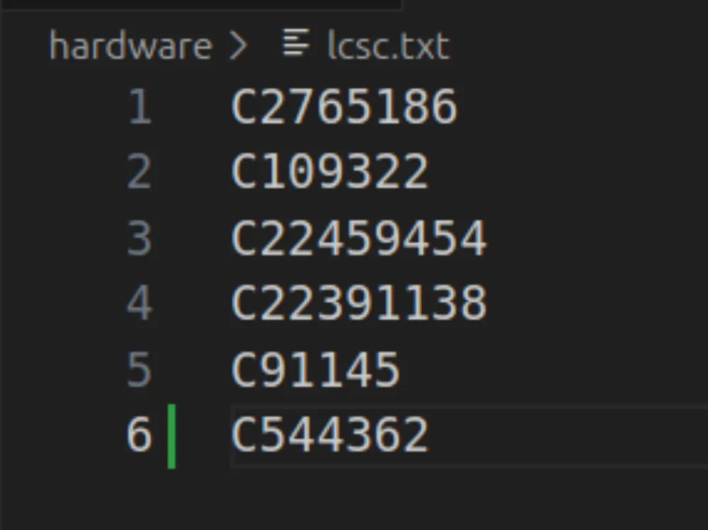
Now after creating both of those files, in your favorite IDE, edit lcsc.txt with the part numbers of the chips that you are going to use.
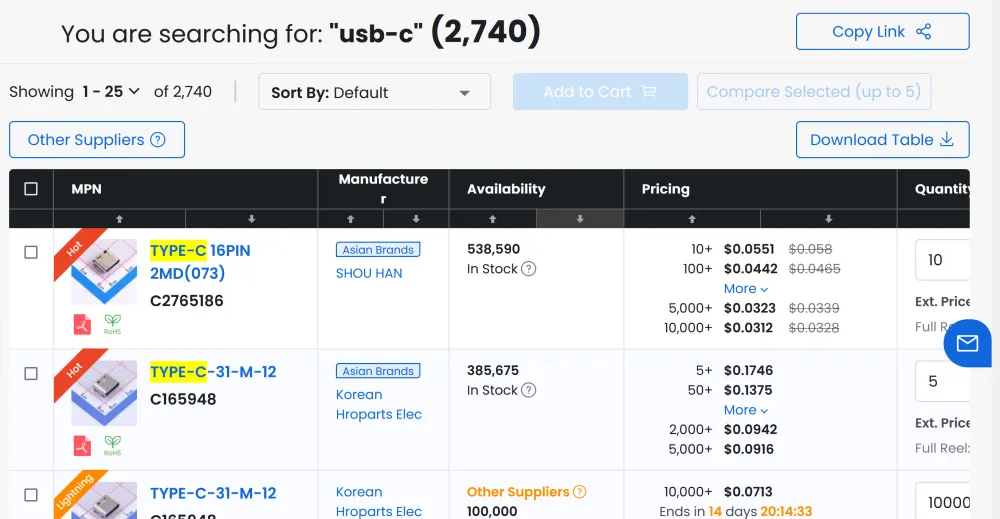
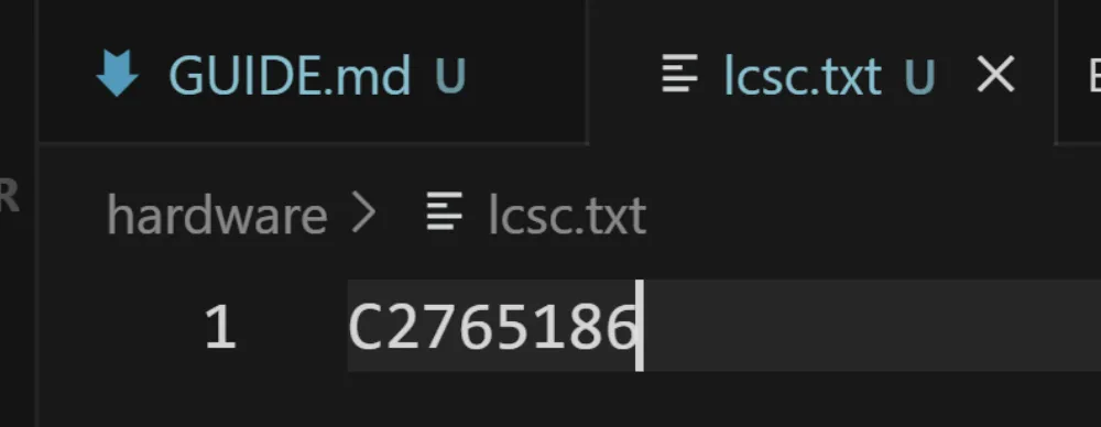
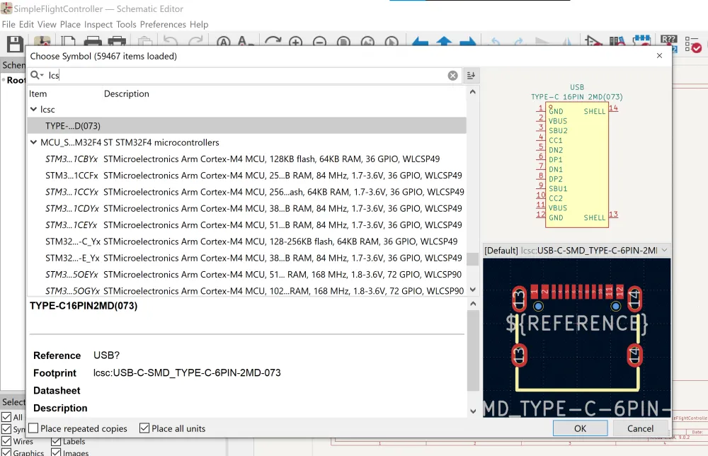
For example, let's say I want to add a USB-C port from LCSC. Go to www.lcsc.com and search for USB-C.
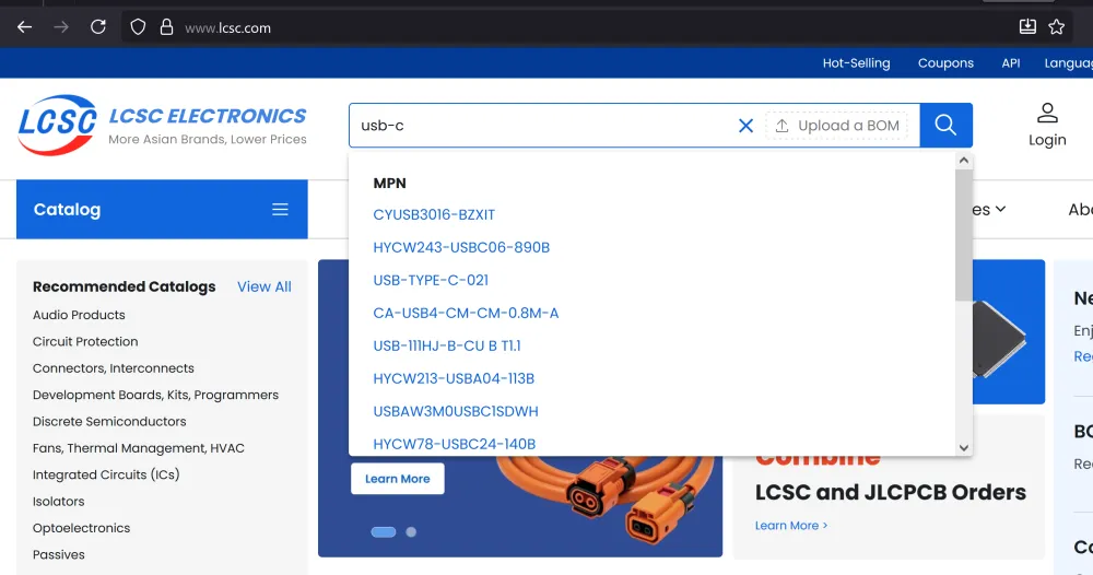
After searching, I found a good part with large stock (important!), so I then copy the part number (always starts with C followed by numbers, and it's under the name) into lcsc.txt.
It should look like this:
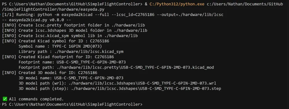
Then run the Python script to convert that part number into a KiCad library. IMPORTANT: YOU NEED TO RUN THE SCRIPT EVERY TIME YOU UPDATE lcsc.txt. If you get an error that you can't find lcsc.txt, make sure to run the file from the root of your project or add arguments to specify the path of the library/lcsc txt file.
If you have done everything correctly, you should have something that looks like this:
If in the future you get an error that the script couldn't find/parse a 3D model, those errors are safe to ignore as you can add the 3D model later. However, if the script can't find/parse a footprint for a specific part, then you should probably find another one on LCSC.
After running the script for the first time, add the library to your KiCad project and also the footprint library (the folder that ends with .pretty). It should look like this when you are done.
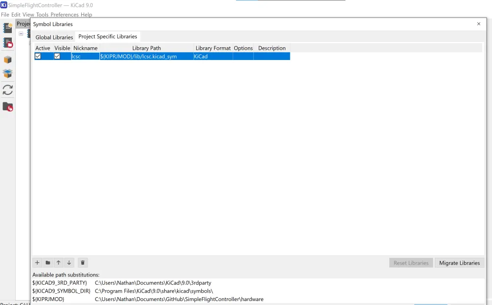
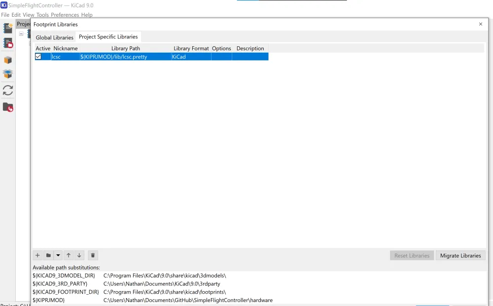
Then after that's done, go into your schematic and search for "lcsc". You should find the library with the USB-C connector (or whatever other part you imported).
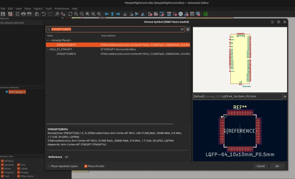
Keep in mind that there are some parts that KiCad already has, such as STM32F722RETx, but there are others like the IMU that you will have to import.
After finding the components on LCSC, my lcsc.txt looks like this:
Now run the script again. Once it's done, go back to KiCad and add in all of the components (you may have to reopen the choose parts screen for the LCSC library to update).
USB-C and Power
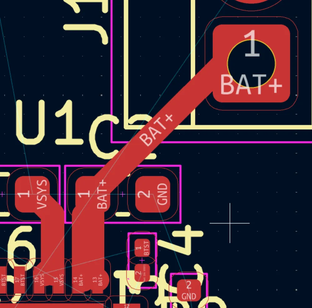
Now let's start wiring up the power components and USB-C. It's always good practice to start wiring the components that would be used first. In this case, it would be USB-C as it is going to receive voltage, then the battery connector as that voltage from USB-C is going to directly charge the battery. If there is no USB-C, then the battery will provide voltage, followed by the 2 regulators. Again, you can wire each component up in whatever order. I just do it like this to be a bit more organized.
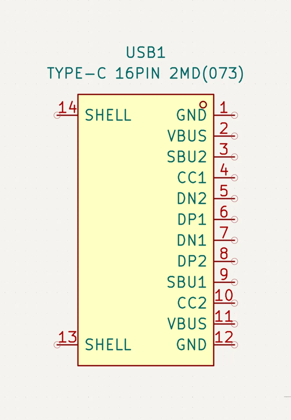
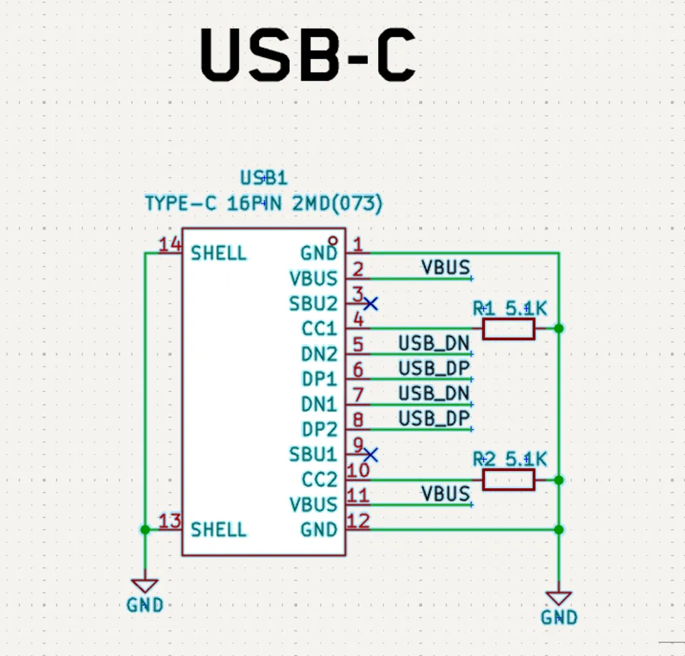
This is the USB-C connector. As you can see, it has a lot of pins, but don't worry if you don't know what all of those mean. Here's a quick explanation:
- Shell: This is the outer case of the USB-C port. It's usually connected to ground.
- GND: Ground.
- VBUS: This is the pin that supplies voltage from the device that connects to it. Usually it provides 5V at 3A, depending on the cable.
- SBU1/2: These are low-speed lines that can be used as alternate pins for different accessories, such as AUX+ and AUX- when connected to a DisplayPort. We don't need to use them.
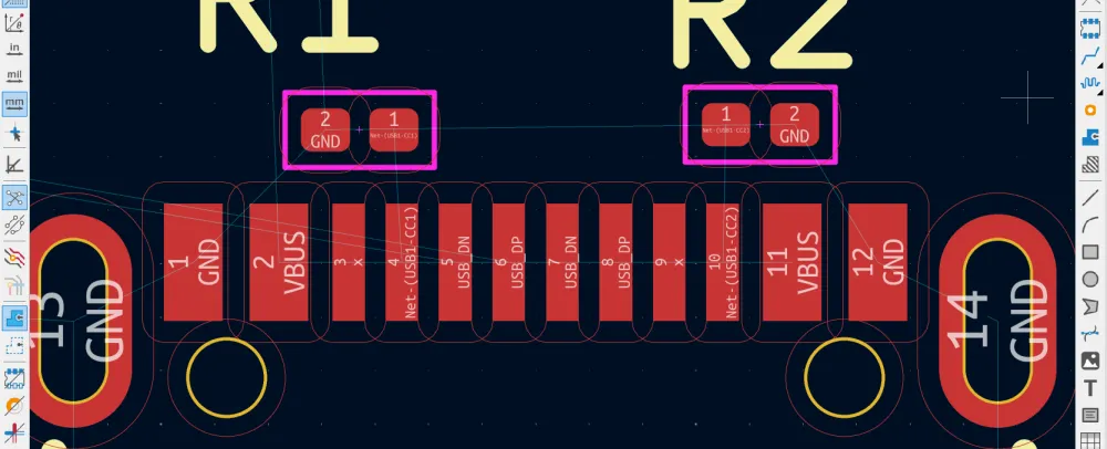
- CC1/2: These are Configuration Channel pins. Basically, they detect if the connector is flipped and can also be used to negotiate more power out of VBUS (USB-PD). We are going to connect them to 5.1K resistors to ground as this tells the other device that we want 5V.
- DN/DP: These are the USB lines that we will be connecting to the STM32. They are used to transfer data between devices.
Now with that information in mind, when you finish wiring up the USB-C connector, it should look like this:
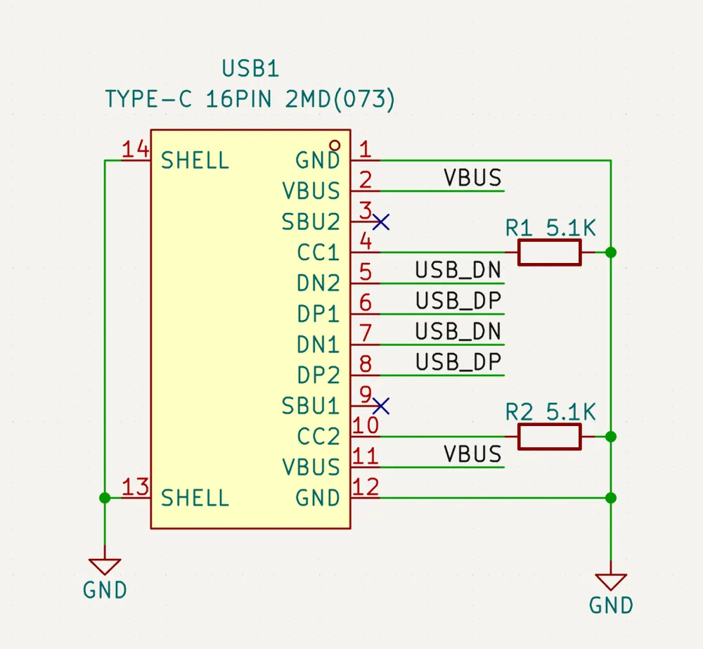
I used net labels to organize it better so that we don't have spaghetti cables all over the schematic.
Battery Charger (BQ25883)
Now let's wire up the battery charger. This is the next step in our power route. There are many chips in the world, and knowing the pins on each of them is virtually impossible. So, each manufacturer provides what's called a datasheet for each component. It's basically a document that details everything about that chip—its pinout and how to implement it.
To access the datasheet for any component in KiCad, simply click on the component and press D. If there isn't one, just search on Google "[part] datasheet" and it's usually a PDF.
Opening the datasheet for the battery charger, we are greeted with this:
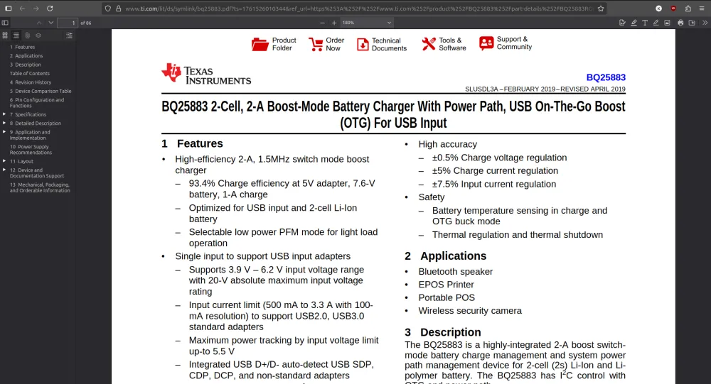
This may look intimidating as there are 86 pages of letters, numbers, formulas, and graphs. However, there is one section that is valuable to us called Application and Implementation. This section basically gives us a reference schematic on how to use said chip. We can use the sidebar or table of contents to locate that section. You should see this:
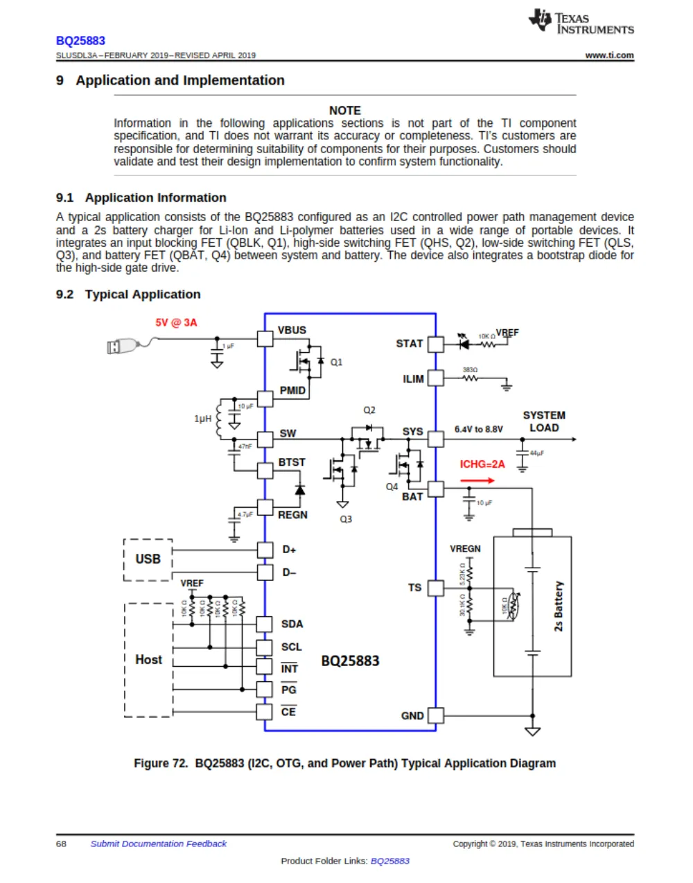
This is the schematic for a specific implementation, and we can see below that there is a table that describes it:
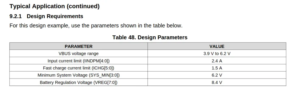
Here we can see the different parameters that influence the design of the schematic above. It is important to understand what each of these values means to determine if the schematic works for your specific needs.
Design Parameters Explained:
- VBUS voltage: How much voltage the chip needs to charge the battery. Our 5V from the USB-C fits within the range, so we're good.
- Input current limit: Determines how much of the available 3A current will be consumed.
- Fast charge current limit: Sets how much current will be used to charge the battery.
- Minimum system voltage: If the battery falls below this voltage, the internal regulator activates to maintain this voltage until the battery completely dies.
- Battery regulation voltage: The maximum voltage the chip will charge the batteries to. In this case: 4.2V per Li-ion cell × 2 cells = 8.4V maximum.
These parameters determine the specific resistor and capacitor values needed in the schematic. If we scroll down further in the datasheet, we can see the calculations needed to determine the inductor and capacitor values:
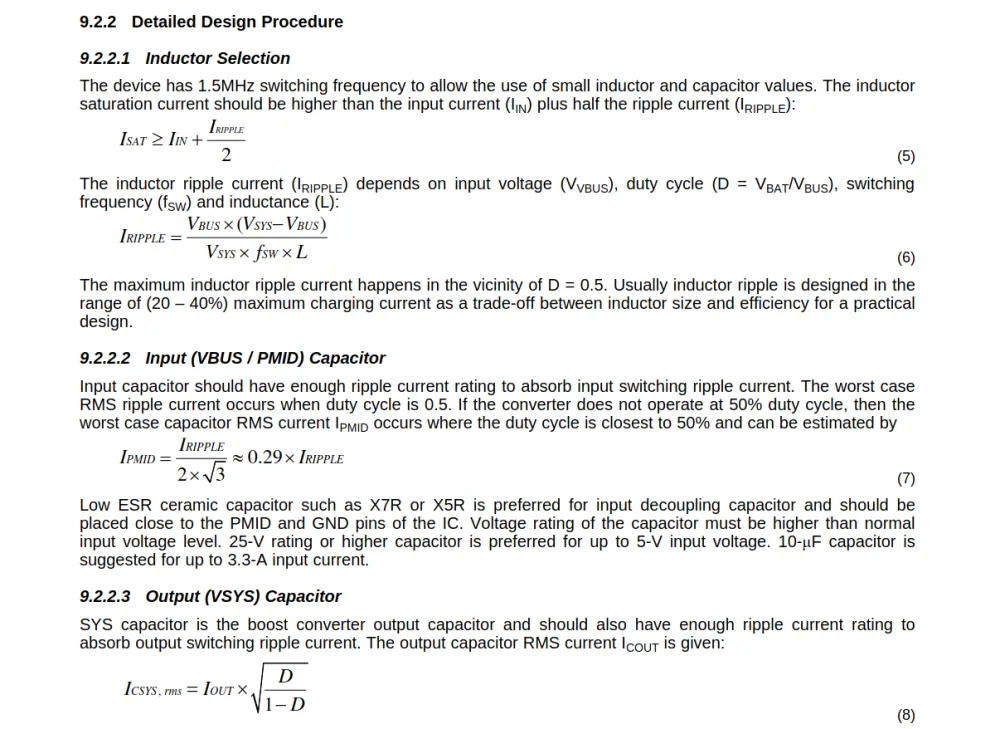
If you need a chip that has a reference schematic that doesn't fit your needs, then you need to do some calculations in order to get the right component values. However, usually you don't have to do that.
Extra Info
If you haven't noticed already, the chip can be connected to a host through some pins called SDA, SCL, INT, CE, and PG. If you don't know what they do or want to know what they mean, there's a section in the datasheet called Pin Configuration and Functions that goes into detail about what each pin does.
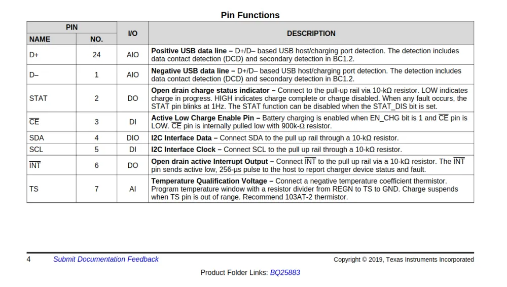
Here we can see that for those pins there are descriptions like active low, open drain, and I2C. Let's break down what these terms mean:
Active Low
Active low means the pin is "active" (doing its job) when the voltage is LOW (0V or close to ground), not when it's HIGH (3.3V or 5V). Think of it like a backwards switch—when you pull the pin to ground, that's when it triggers the function. Many reset pins work this way: pull the reset pin low to reset the chip, and let it go high to run normally.
Open Drain
Open drain is a type of output that can only pull a pin down to 0V (LOW), but cannot push it up to 3.3V (HIGH). Think of it like a one-way switch—it can only connect the wire to ground, not to power. When the switch is "off", the wire is left floating with no connection. This is why open drain pins need a "pull-up resistor"—a resistor that connects the wire to 3.3V and keeps it HIGH when nothing is pulling it down. Multiple chips can share the same wire this way without interfering with each other.
Communication Protocols
Now let's talk about the different ways chips can talk to each other. There are several common protocols you'll encounter:
I2C/I3C (Inter-Integrated Circuit)
I2C uses only 2 wires: SDA (data) and SCL (clock). Multiple devices can share the same two wires, and each device has a unique address. Think of it like a conference call where everyone shares the same phone line, but each person has a unique ID. Both wires need one pull-up resistor each (in total) in order to function correctly.
Pros:
- Only needs 2 wires regardless of how many devices you connect.
- Built-in addressing system allows multiple devices on same bus.
- Relatively simple to implement.
- Good for sensors and simple peripherals.
Cons:
- Slower than SPI (typically 100 kHz to 3.4 MHz).
- Limited distance—long wires can cause signal problems.
- Can get complex with timing issues and error handling.
- Address conflicts if two devices have the same address.
SPI (Serial Peripheral Interface)
SPI uses at least 3 wires plus one additional wire for each device: MISO (Master In, Slave Out), MOSI (Master Out, Slave In), SCK (clock), and CS (Chip Select) for each device. It's like having separate phone lines for each conversation.
Pros:
- Much faster than I2C (can go 10 MHz+ easily).
- Full duplex (can send and receive simultaneously).
- Simpler protocol.
- More reliable over longer distances.
Cons:
- Needs more wires (especially with multiple devices).
- No built-in error checking.
- Only one master device allowed.
- Can use up many pins quickly with multiple devices.
UART (Universal Asynchronous Receiver-Transmitter)
UART uses 2 wires: TX (transmit) and RX (receive). It's a point-to-point connection between two devices, like a private phone call.
Pros:
- Very simple—just 2 wires.
- No clock signal needed (asynchronous).
- Long distance capable with proper drivers.
- Universal—almost every microcontroller has it.
- Good for debugging and console output.
Cons:
- Only connects two devices directly.
- Both devices must agree on baud rate (how fast the data goes) beforehand.
- No built-in error correction.
- Can lose sync if timing is off.
USB (Universal Serial Bus)
USB uses 2 data wires (D+ and D-) plus power and ground. It's like a smart postal system that can handle packages of different sizes and priorities.
Pros:
- Standardized connector and protocol.
- Provides power to devices.
- Hot-pluggable (can connect/disconnect while powered).
- High speed (up to 10 Gbps on USB 3.1).
- Built-in error correction and flow control.
- Can connect many devices through hubs.
Cons:
- Complex protocol requiring dedicated hardware/software.
- More expensive to implement.
- Requires specific connectors and cables.
- Power management can be tricky.
- Not suitable for real-time applications due to variable latency.
We will not be connecting the USB to the battery charging chip as we need to connect the STM32 to USB-C to be able to program it. Looking through the datasheet, it says that those pins are used to determine how much current can be used. However, they can also be set through the I2C interface that the IC has, so we can change that later with the STM32.
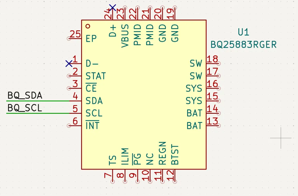
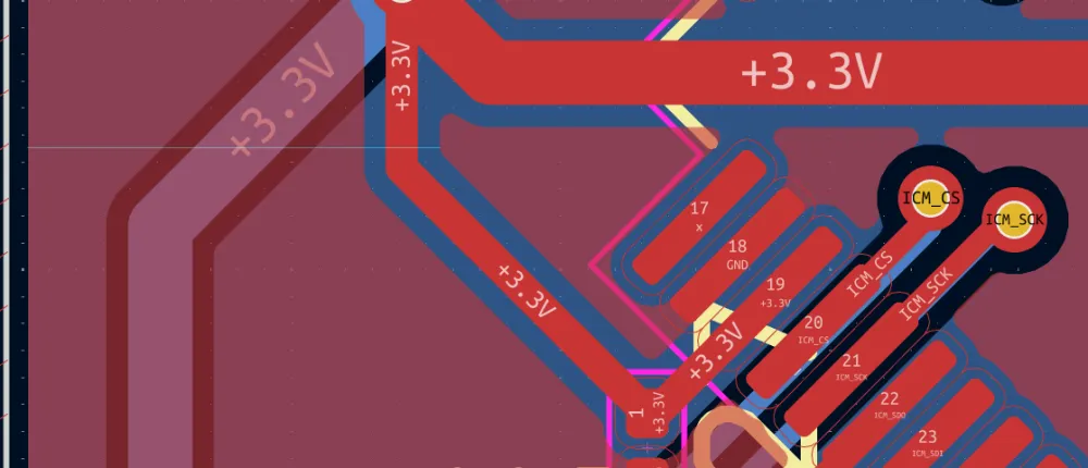
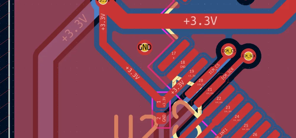
Now that we know that the schematic suits our needs, we can start copying it in KiCad. When copying a schematic from a datasheet, any pins that can be connected externally should use Net Labels like so (obviously with the pull-up resistors added later):
Also, because we are dealing with power, we have to use separate grounds such as power ground and digital ground. Usually, for most chips, we will use the digital ground. However, sometimes we have to work with power components and need to have a cleaner ground reference. In the datasheet, you can see that there are different symbols for ground.
Digital ground is used for all the digital components like microcontrollers, sensors, and logic chips. Digital circuits switch on and off rapidly, creating noise on the ground plane. This is fine for digital circuits since they only care about HIGH (1) or LOW (0), not the exact voltage.

Power ground is used for high-current circuits like motor drivers, charging circuits, and voltage regulators. These circuits can draw lots of current, creating voltage drops and noise in the ground connections. Keeping them separate prevents this noise from affecting sensitive circuits.
Why Separate Them?
The noise from digital switching or high-current power circuits can interfere with sensitive analog measurements from the sensors.
The trick is to keep these grounds separate on the PCB traces but connect them together at a single point. The datasheet says to connect them below the thermal pad (a conductive area under ICs to dissipate heat/reduce noise) of the chip. This gives each type of circuit its own clean ground reference while still maintaining a common ground for the entire board.
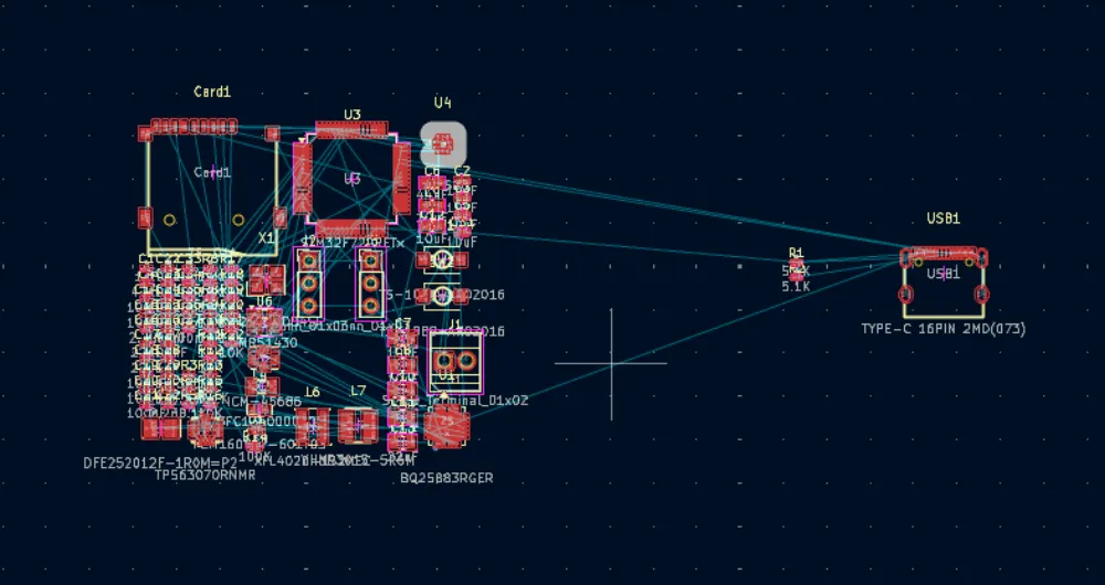
Now wire up the rest of the schematic, and you should end up with something similar to this:
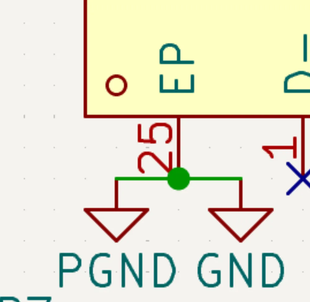
Note the mess, but I have different ground names for PGND and GND, although I used the same symbol. I added a battery screw terminal and also connected the battery ground to PGND, and I also shorted PGND and GND. I plan on connecting PGND and GND on the bottom of the thermal pad (this is actually the EP/Pin 25, but in the end I removed PGND and used only GND for simplicity).
Regulators
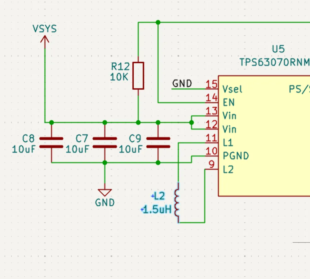
Now after finishing the battery charger, I am going to start wiring up the regulators, starting with the TPS63070.
Apply the same methodology as wiring up the battery charger: look up the datasheet, go to the Application and Implementation section, and look at the schematic. In this case, there are 2 schematics:
A typical application that can be adjusted depending on your needs.
And if you scroll down a bit more:
Another typical application, but this time it outputs a fixed voltage.
Really, the only difference is that for the adjustable version, there's a voltage divider—a pair of resistors that can be used to create a voltage less than or equal to the input voltage:
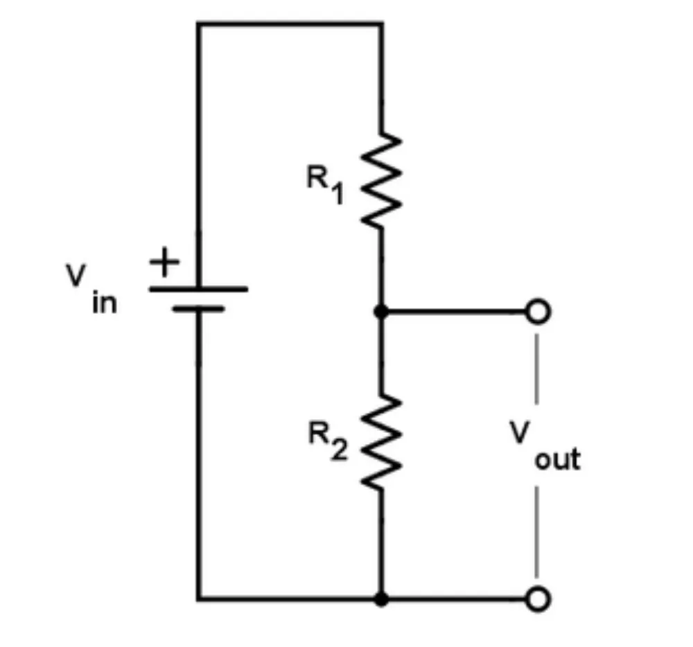
In the fixed version, we don't use a voltage divider so it stays at 5V (it's predetermined in the chip).
In our case, we are going to use the fixed version as it uses fewer components and also gives us the 5V that we need.
TIP
When wiring things based on schematics, make sure to use the recommended size capacitor/inductor values (if mentioned) and set it in KiCad like so when you are going to place the part:
Using the fixed schematic (and taking into account the correct footprint sizes), wire it up in KiCad. You should get something like this:
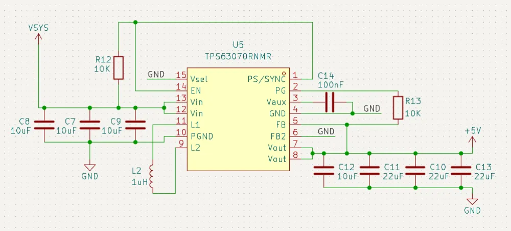
With VIN connecting to VSYS (battery or USB voltage) and VOUT connecting to +5V. Separate grounds are not needed here, so they are GND.
If you don't know what footprint size to add to the other components (resistors, inductors, etc.), don't worry. We will revise this later.
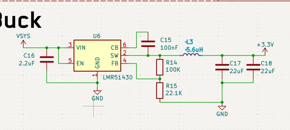
Now moving on to the final power part, the LMR51430.
Repeat the same as the other 2 parts: open the datasheet and look for the Application and Implementation section. Switching regulators (like the name implies) switch MOSFETs (tiny gates) open and close very fast in order to regulate voltage. This can be measured by the switching frequency of the chip. In this case, we have 2 tables under the schematic.
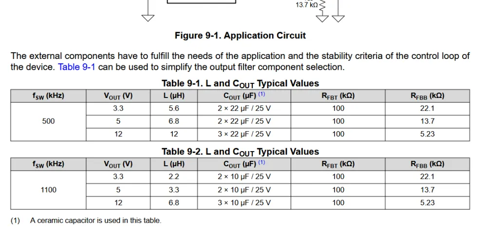
One for a switching frequency of 500 kHz and another one for 1.1 MHz (1100 kHz). With a higher switching frequency, it is less efficient and also can produce more heat. However, overall, the space it takes up is less than with the lower frequency. On the other hand, a lower switching frequency is more stable/efficient and doesn't heat up as fast. It also produces a lot less noise (which is what we need). So in this case, we will go with the lower switching frequency at 3.3V. If you want to wire it up based on the higher frequency, then feel free to do so. Just take into account the pros and cons of each one. (All of this information is from the datasheet, by the way.)
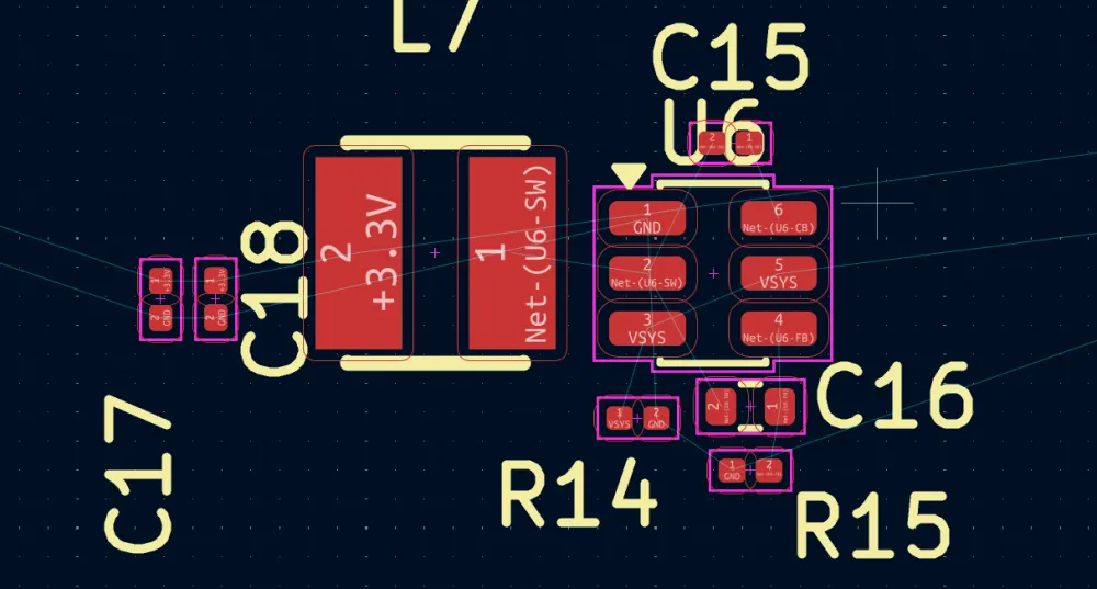
After routing it, you should get something like this (for a 500 kHz switching frequency at 3.3V):
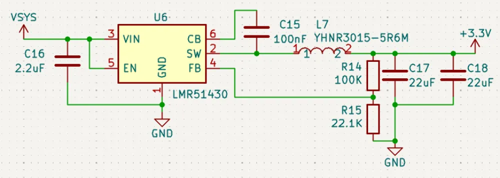
Like the 5V regulator, VIN = VSYS, but VOUT = +3.3V as this chip is giving us 3.3V output.
Double-check the values on the resistor divider as that is what determines the output voltage. Also, in the reference schematic, it shows one capacitor of 44 µF, but in the table, it's 2 capacitors of 22 µF, so I used those.
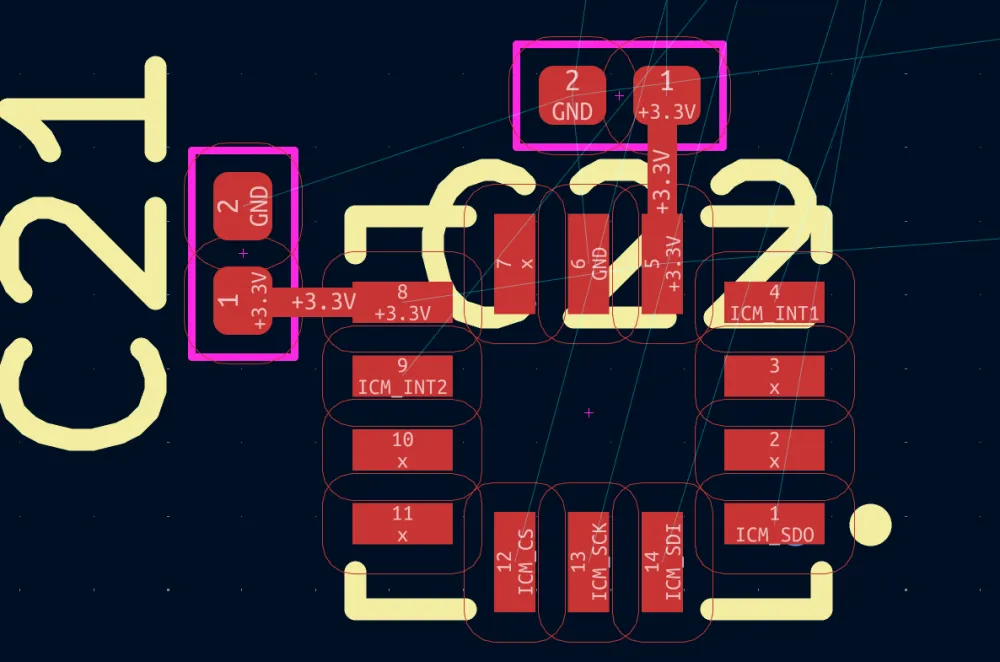
Sensors and Peripherals
Now that we've got power out of the way, it's time to route the sensors and the microSD.
BMP580
Starting with the BMP580, when I try to open the datasheet, it says that no datasheet is defined. So you have to look it up on Google and found this.
Looking around the table of contents, there is no Application and Implementation section, but there is a Pinout and Connection Diagrams which is close enough:
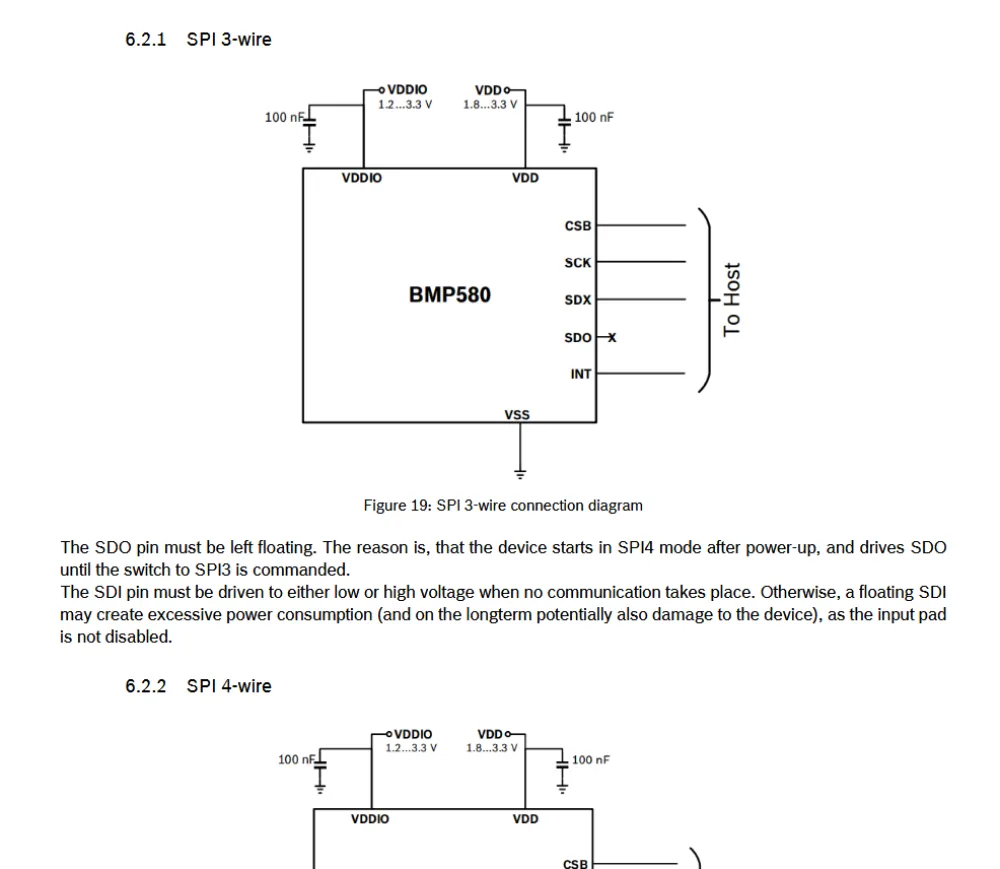
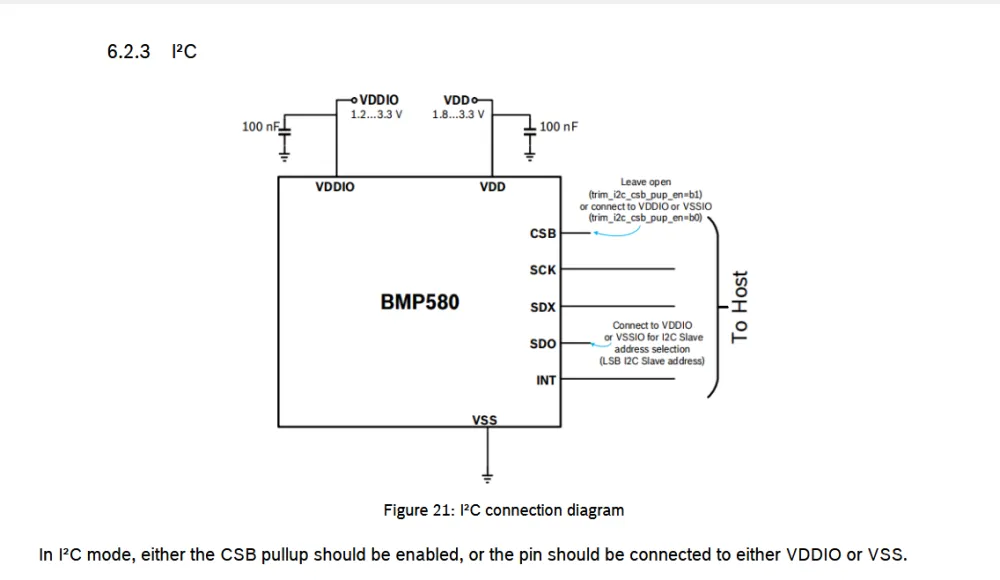
Taking a look at the different schematics, there are different ways of connecting the chip through SPI, I2C, and I3C. Above in the Communication Protocols section, I explained what each of these mean. For this chip, I plan on using I2C as it's the default mode of communication for this chip. (This is personal preference; feel free to use whichever mode of communication you wish.)
When implementing I2C, you need to have pull-up resistors on each line. However, if you recall, the battery charging circuit uses I2C as well, and we already put pull-up resistors there, so it isn't necessary to add them here.
Following this schematic, after wiring it up in KiCad, you should get this:
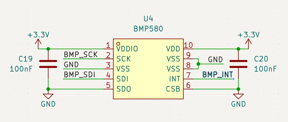
I wired both VDD and VDDIO to 3.3V as that is the voltage that all of the other chips are running at (microcontroller and sensors).
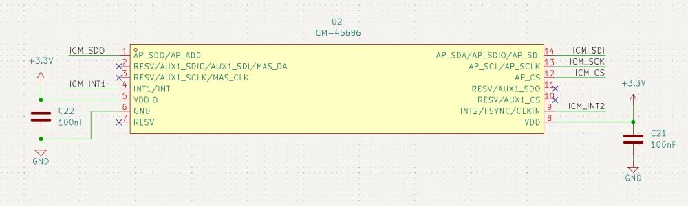
ICM-45686
Looking at the ICM-45686 datasheet, it has different modes of operation like the BMP580. However, the one that interests us is this one:
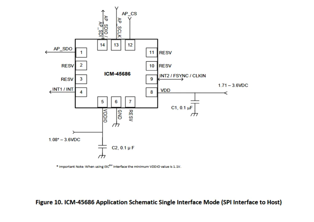
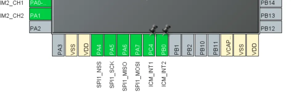
Changing things up a bit, we are going to connect the sensors to the microcontroller through SPI. This gives us the advantage of faster data and also allows us to learn how to implement it later on in code.
Also, in the schematic, looking at pin 14, it serves the dual purpose of being a SDIO or SDI. However, in our case, we want to use it as SDI to use the full capacity of SPI.
You should end up with something like this after:
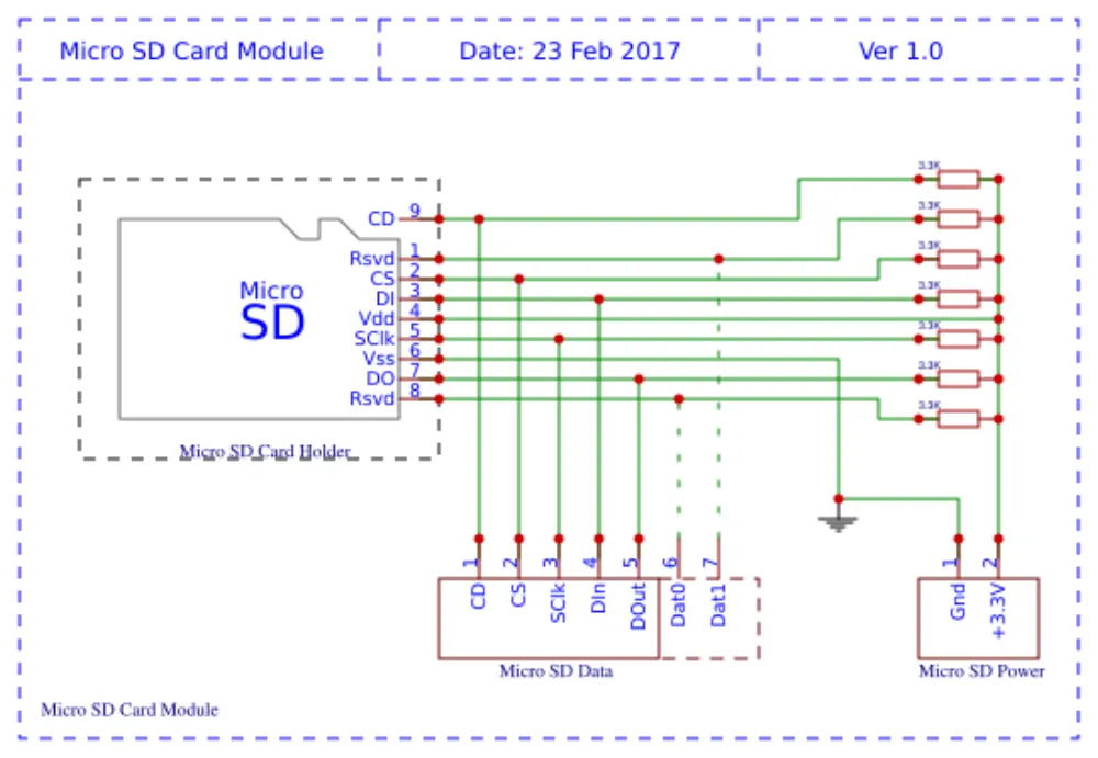
MicroSD Card
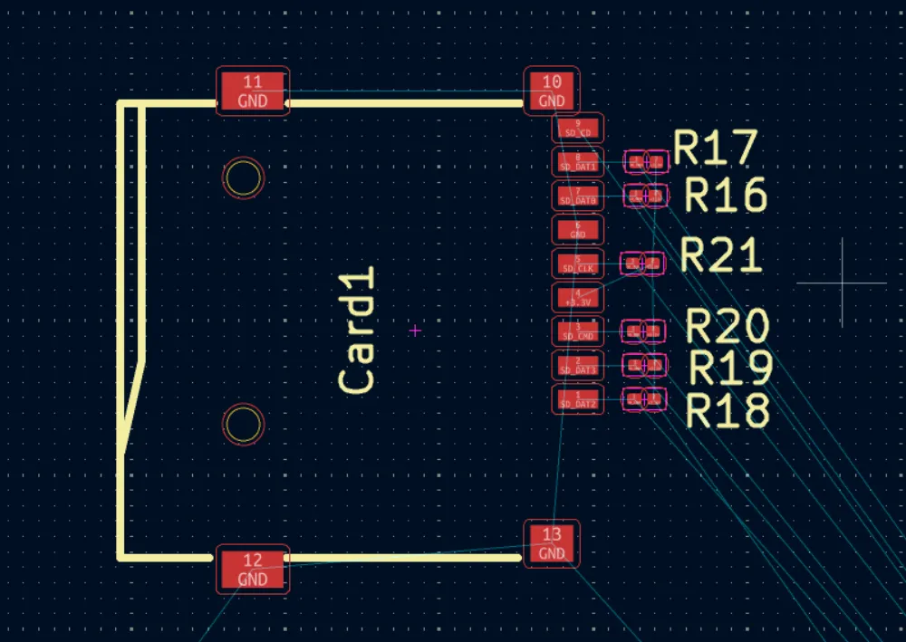
MicroSD works on the same principle as SPI but can have more channels for faster data throughput. This form of communication is called SDIO (Secure Digital Input Output) and can work in 1-bit or 4-bit data modes (4-bit has more channels and faster data transfers).
Here is an example schematic of how the SD card should be wired, but we are going to modify it a bit to fit our needs. There are 8 pins on the microSD, and here's a table showing their meaning:
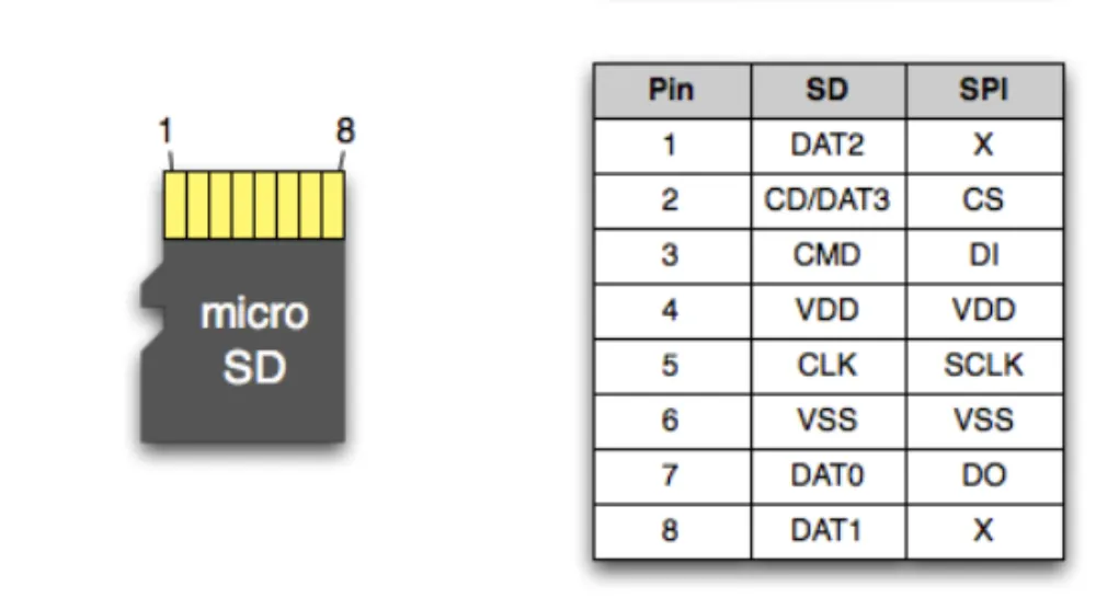
In SDIO (SDMMC) mode, DAT0-3 are used for data transfer, CLK for clock, and CMD for sending/receiving commands between the microcontroller and microSD card. DAT3 can also be considered a CD (Card Detect) pin, but usually, there is a 9th pin on most symbols that uses the case directly to detect if there is an SD card or not.
Another thing to keep in mind when wiring up the microSD card: 10K PULL-UPS ARE REQUIRED FOR EVERY PIN ON THE MICROSD CARD (excluding the 9th pin/GND/VCC).
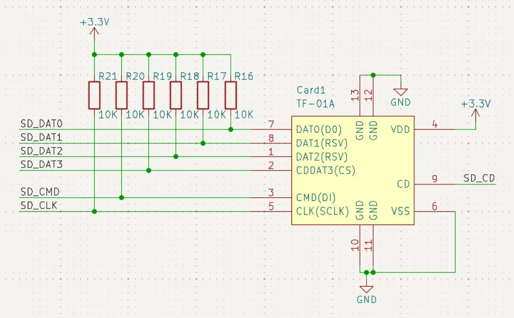
After wiring it up, you should get something like this:
Now all that's left is to connect everything to the microcontroller!
Microcontroller Break
Since we are using an STM32, there is a really cool piece of software called STM32CubeMX. It basically allows you to select the functions and types of communication that you need, and it automatically selects the pins so that we don't have to read the datasheet and get stuff wrong.
To start, download it here and wait for it to install.
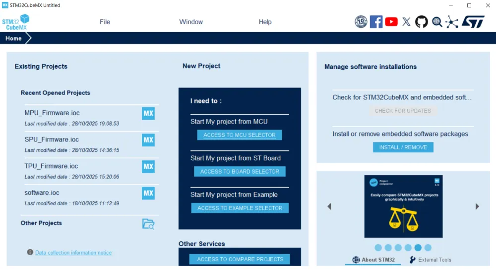
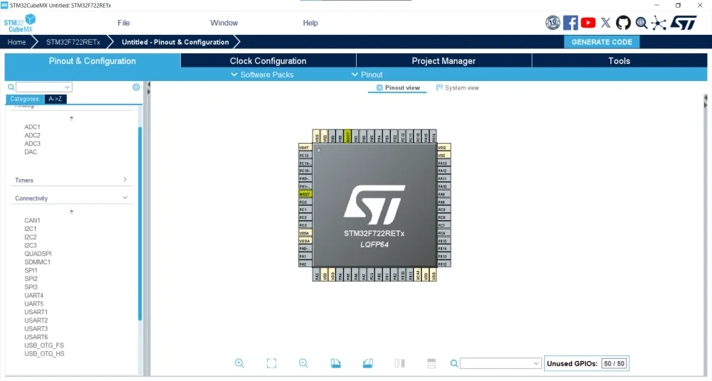
After installing it and opening it, you should be presented with this screen:
Click on ACCESS TO MCU SELECTOR as we are going to create a new project based on the MCU that we are using: in this case, STM32F722RET.
After searching for the MCU, you should see this screen:
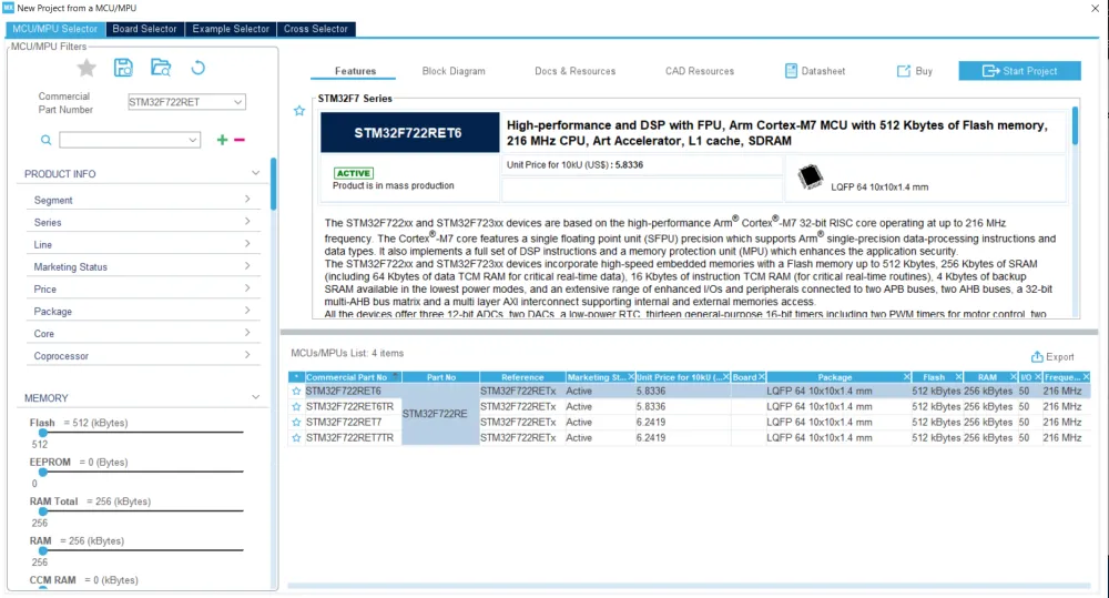
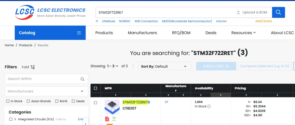
Here, it shows different variations of that version for the STM32, but we are going to select the STM32F722RET6 version as it is the one that has the most in stock on LCSC.
After that, hit "Start Project" at the top. If any windows pop up, say yes.
After loading/downloading the firmware, you should be greeted with this window:
This is where you will be configuring the pinout for the STM32. On the left, you can see the different sections that are able to be configured. However, the only ones that concern us for now are the System Core, Timers, and Connectivity sections.
Connectivity
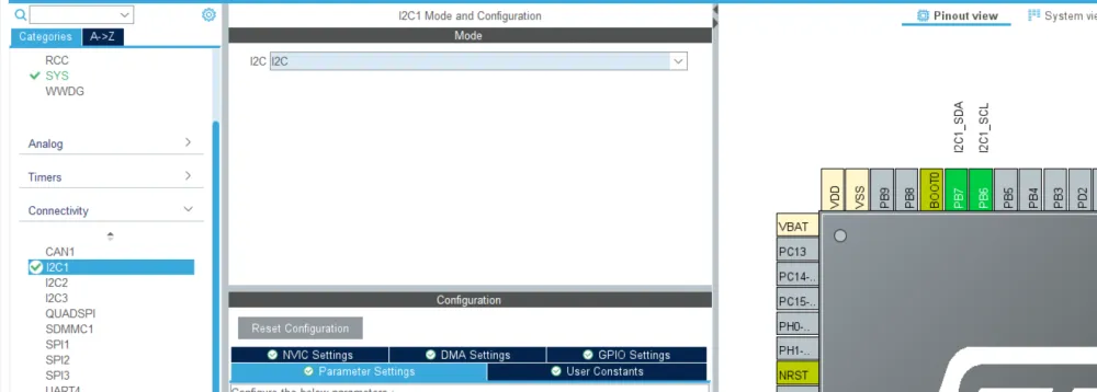
Here, we can see the different ways that we can connect the STM32 to different peripherals through I2C, SPI, UART, SDMMC, USB_OTG_FS, and more. For now, enable the first I2C channel. This will be for the battery charger and pressure sensor. It should look like this:
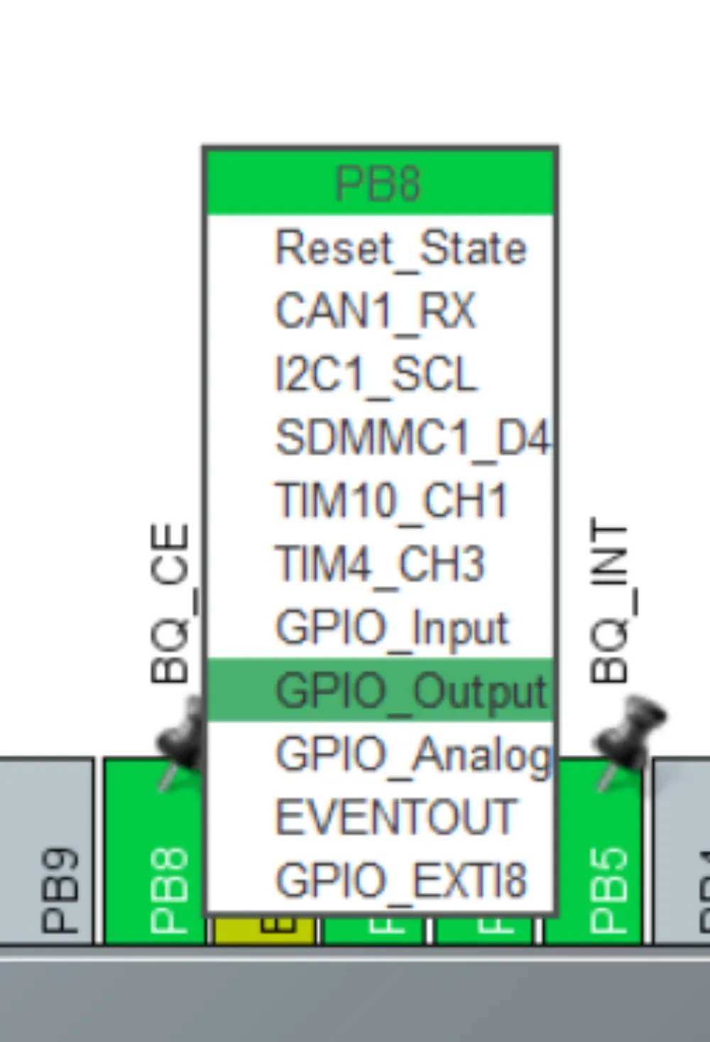
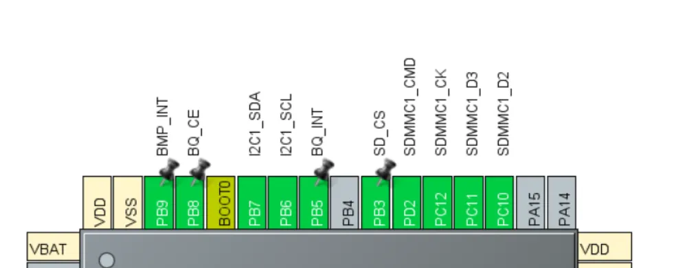
Also, be sure to select pins on either side for the battery charger interrupt and chip enable pins. The BQINT pin should be set as a GPIOEXTIx (x is any number) pin as this lets the STM32 know that this pin is going to be an interrupt pin.
For BQCE, make sure that there's a pin set to GPIOOutput. According to the datasheet, when the pin is low, charging is on, and when it's high, the battery doesn't charge. We can change this later in the code for further customization in case you don't want the battery charge controller running during flight.
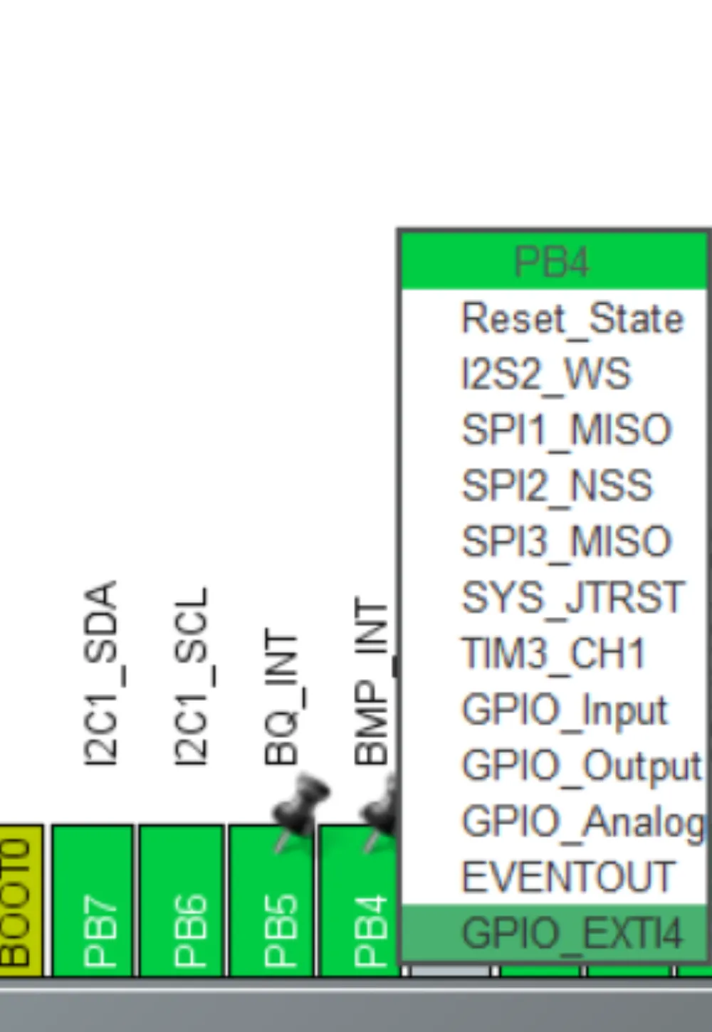
MAKE SURE TO ADD THE INTERRUPT PIN FOR THE BMP580.
When selecting an interrupt, if it deletes another interrupt, choose another pin as some interrupts use multiple pins.
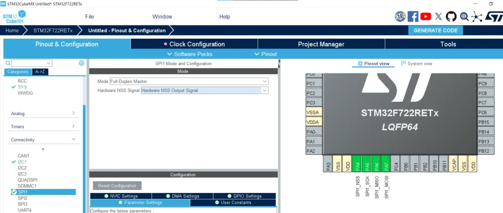
Then enable an SPI channel for the IMU. You are free to use whichever channel you wish, but I am going to select the first one. Select Full Duplex Master as the STM32 will be the master and the IMU the slave, and full duplex because we are using both MOSI and MISO and not just one channel for input/output (half duplex/SDIO). There is also an option under the selection to activate a Hardware NSS Signal. This is used if we have just one device under the SPI bus and makes it so that the STM32 manages the Chip Select pin instead of us having to select a GPIO for it. I enabled it as Hardware NSS Signal Output as the IMU will be the input. After selecting SPI, it should look like this (it can be different if you want to use a different pin for the Chip Select):
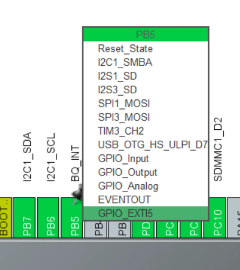
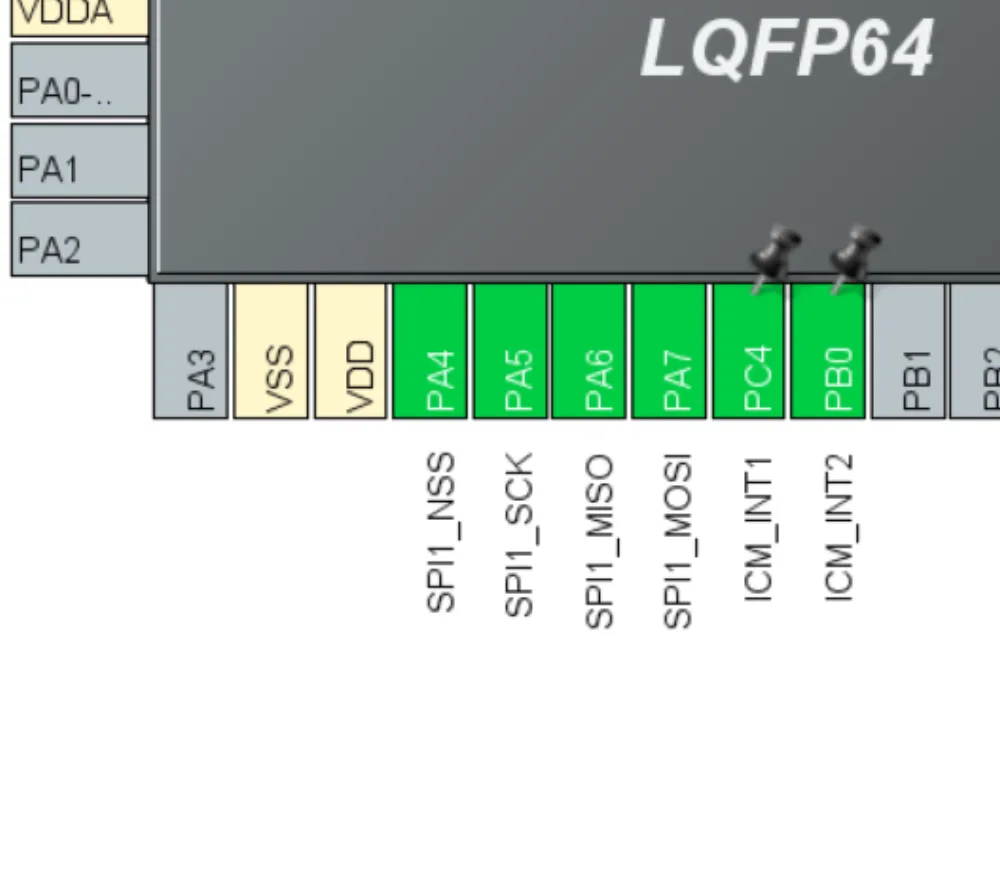
Also, don't forget to add the 2 interrupt pins on the IMU as GPIO_EXTIx (x is any number):
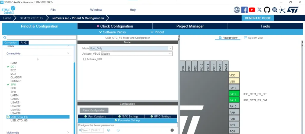
After you've done that, it's time to select USB_OTG_FS. This means USB On-The-Go Full Speed, and it differs from USB_OTG_HS (USB On-The-Go High Speed) as it is slower and doesn't need any extra pins to configure. It's sufficient for our needs of flashing and sending serial data. Set it to host or device (you'll be changing this later depending on your needs). For now, I will leave it as host, and it shows where the USB pins are on the chip.
Now enable SDMMC as this is the communication protocol that we will be using to write/read to our microSD. This should be enabled and set to a 4-bit bus.
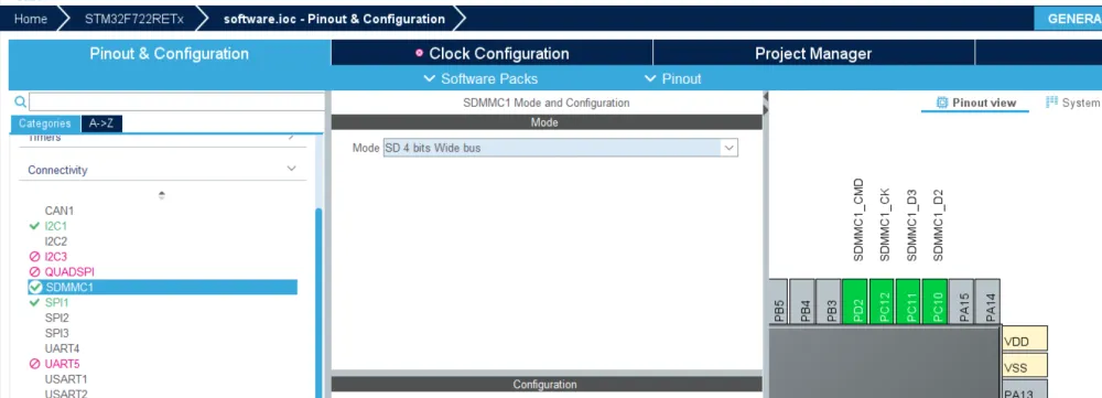
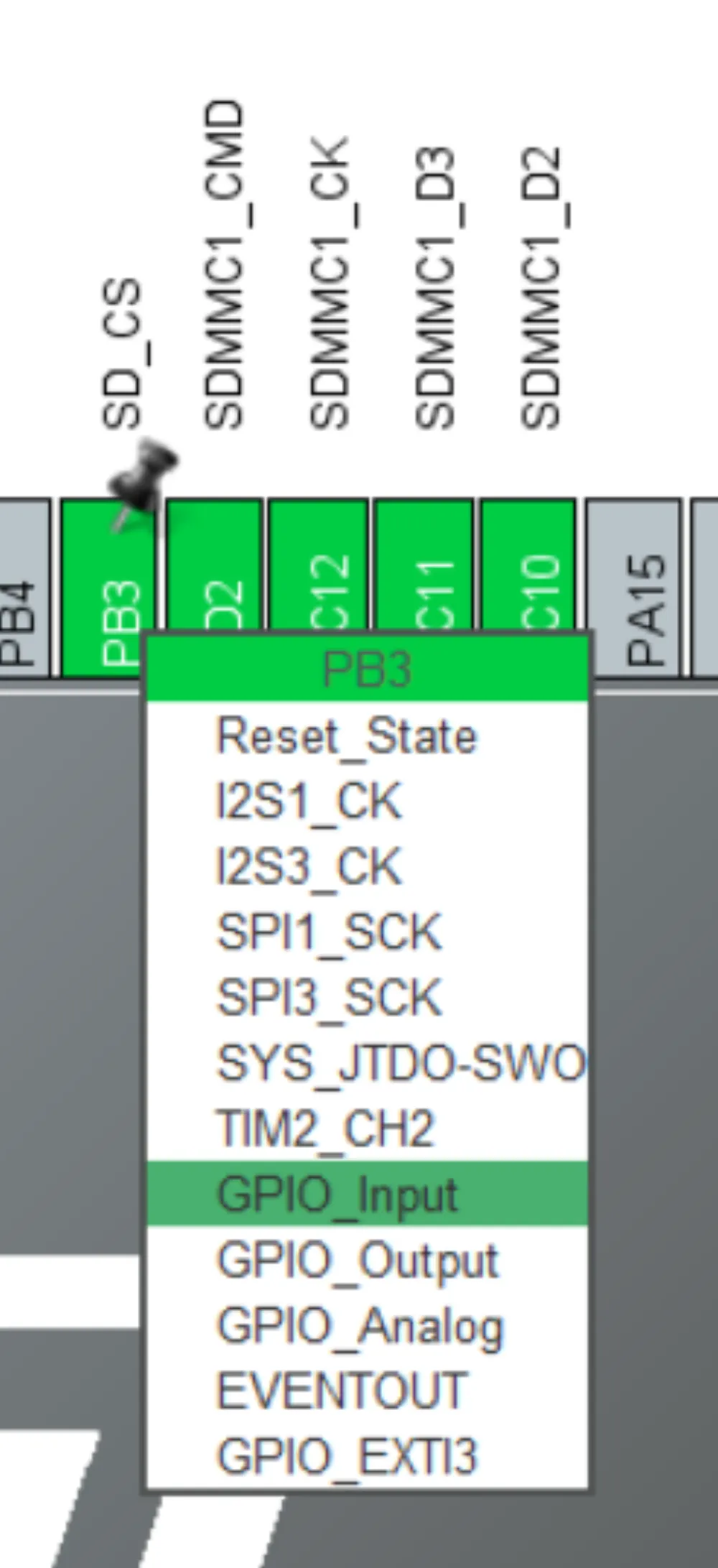
Also, remember to add an extra pin next to it for the card detect pin and make it a GPIO_Input:
Now that we are done with our peripherals/sensors, we are going to configure some other stuff that would be important in starting the STM32 and configuring the servos.
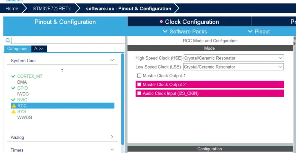
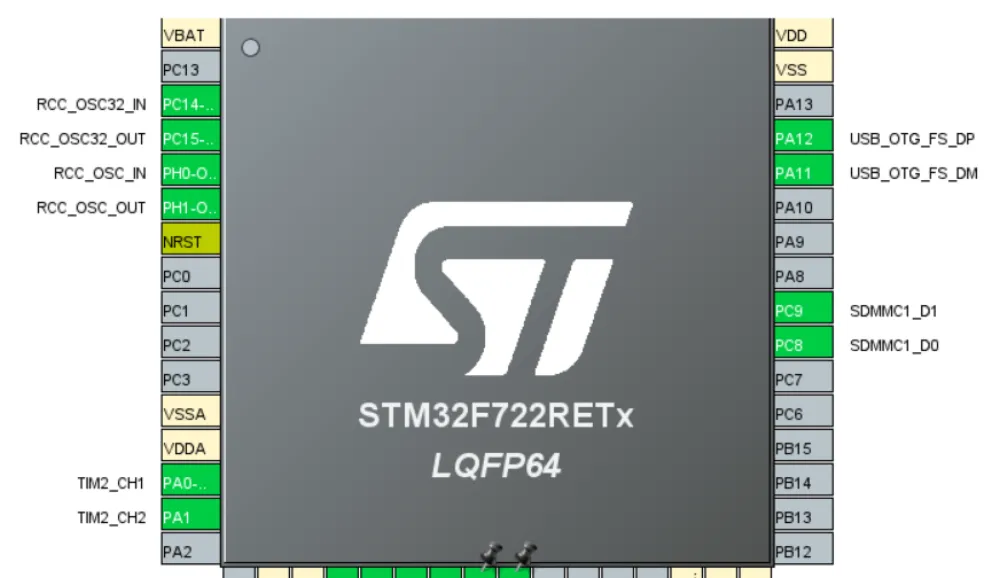
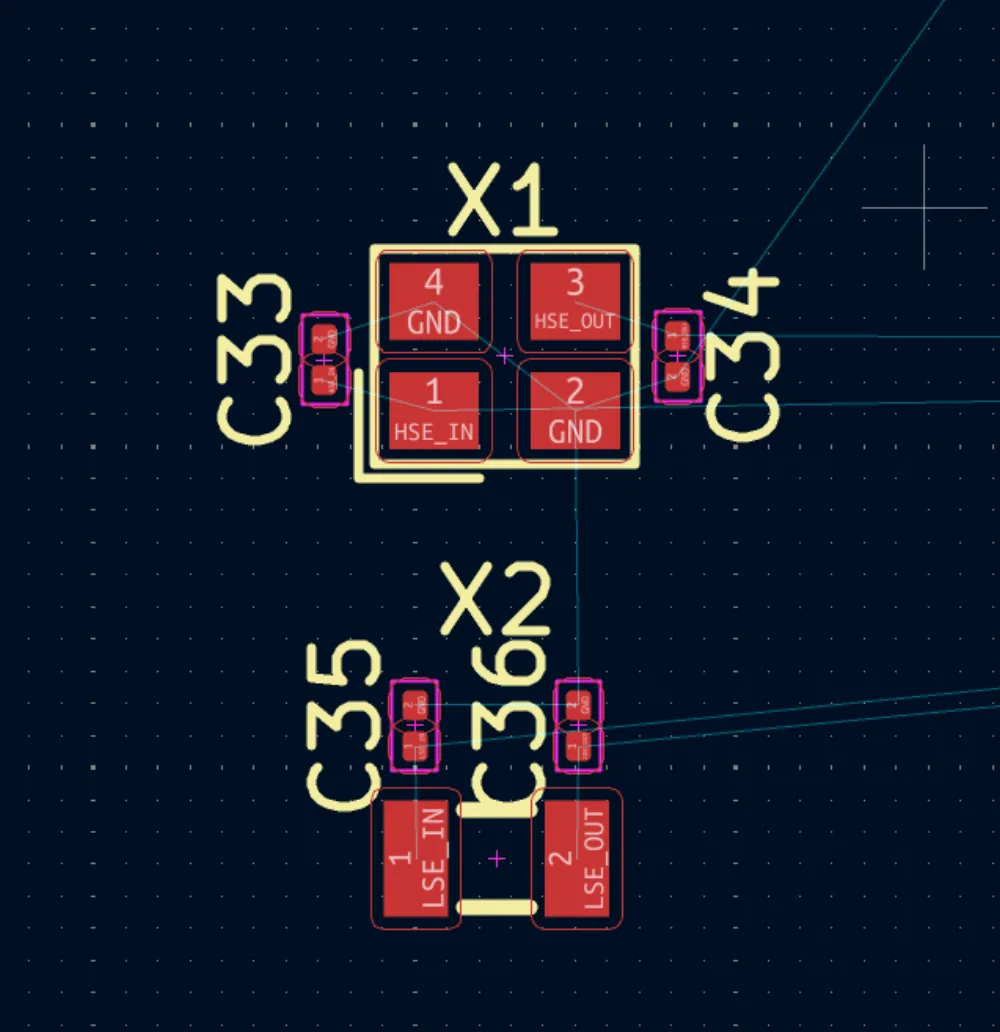
Go to the System Core tab, then click on RCC, and set both the high-speed clock and low-speed clock as a crystal/ceramic resonator. By doing this, we are telling the STM32 that we will have some external clocks that it can use to achieve faster/stable clock timing throughout the entire chip. We will edit this in KiCad later along with the pins.
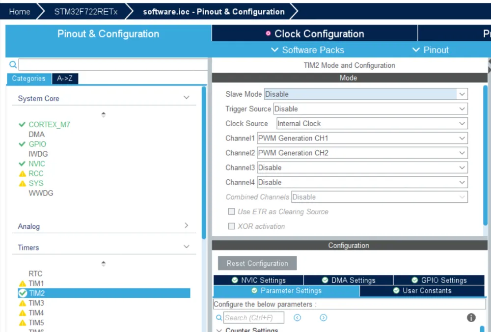
Now go to the Timers section. Here is where we can edit the PWM pins for the servos. Select any timer that has channels that support PWM and select 2 PWM Generation CH channels. We will be able to edit the duty cycle later in the firmware. Also edit the Clock Source and set it to the internal clock. This is needed for the PWM generation as it needs a clock to time the signals correctly.
MAKE SURE TO SAVE USING CTRL+S AND CREATE A NEW FOLDER IN THE ROOT OF YOUR GITHUB REPOSITORY CALLED firmware OR firmware.
This is how my STM32 looks after selecting all of the pins:
Keep this open while we configure the rest of the microcontroller in KiCad.
Back to KiCad
Now after adding all of the pins and peripherals and knowing which pins you are going to use, we are going to finish wiring up the STM32 with what's called a reference schematic. If you want to learn more about this specific type of chip or any STM32 MCU in general, there is a documentation tab (example) that shows you all the implementations/peripherals that you can have with the STM32. After scrolling around, I found a reference design to use with our STM32.
Going to the section named Reference Design, we are greeted with this:
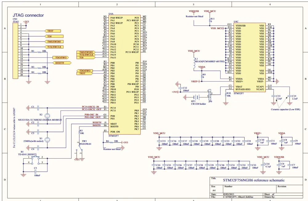
Wiring up Power
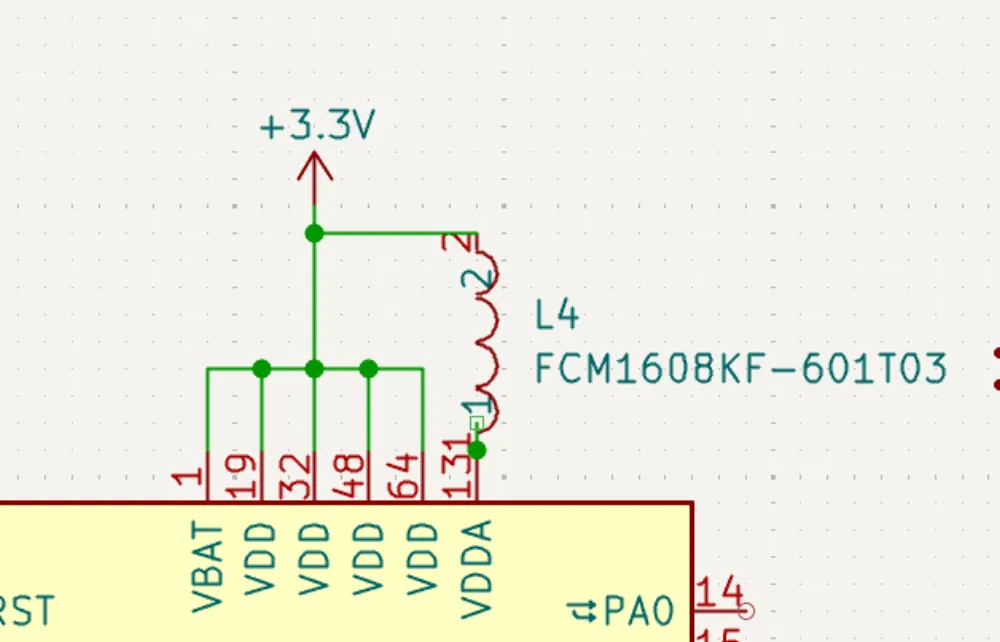
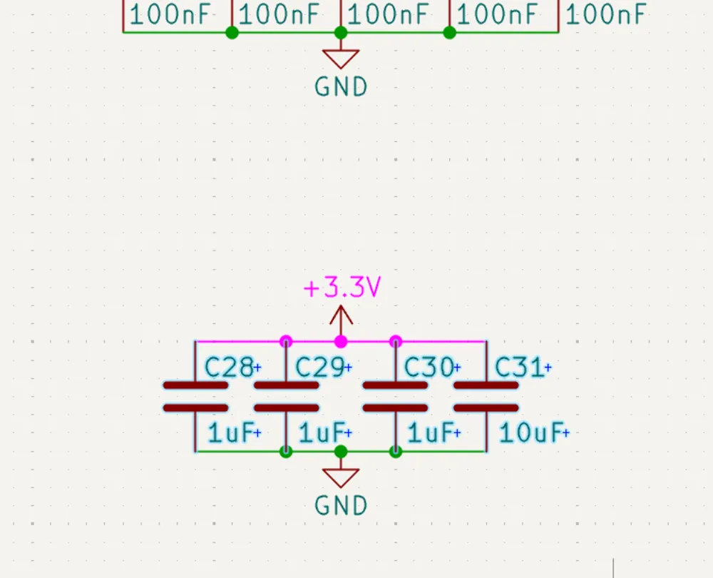
Starting with the decoupling capacitors (capacitors that are placed near ICs to stabilize voltage on power supply lines—they are in parallel with voltage and connect to ground), it is generally good practice to place one 100 nF per VDD pin and then use a bigger 1 µF capacitor per section (e.g., VDD/VDDA/VBAT). Finally, finish off with a big 4.7 µF or 10 µF capacitor on the main voltage line before the STM32 to handle larger voltage spikes. If you have analog voltage (VDDA), it's also good practice to put a ferrite bead (like a capacitor, but it suppresses high-frequency noise currents) before connecting it to VCC to prevent noise from digital switching from interfering with sensitive analog functions.
It is also needed to place a 2.2 µF capacitor in series with VCAP and GND.
VERY IMPORTANT: PUT A 2.2 µF DECOUPLING CAPACITOR ON EACH VCAP PIN OF THE STM32 OR IT WON'T BOOT UP. (From experience)
Based on this information (and the schematic), try to wire up your STM32's VDD/VSS pins (VSS is GND, by the way). You should get something like this:
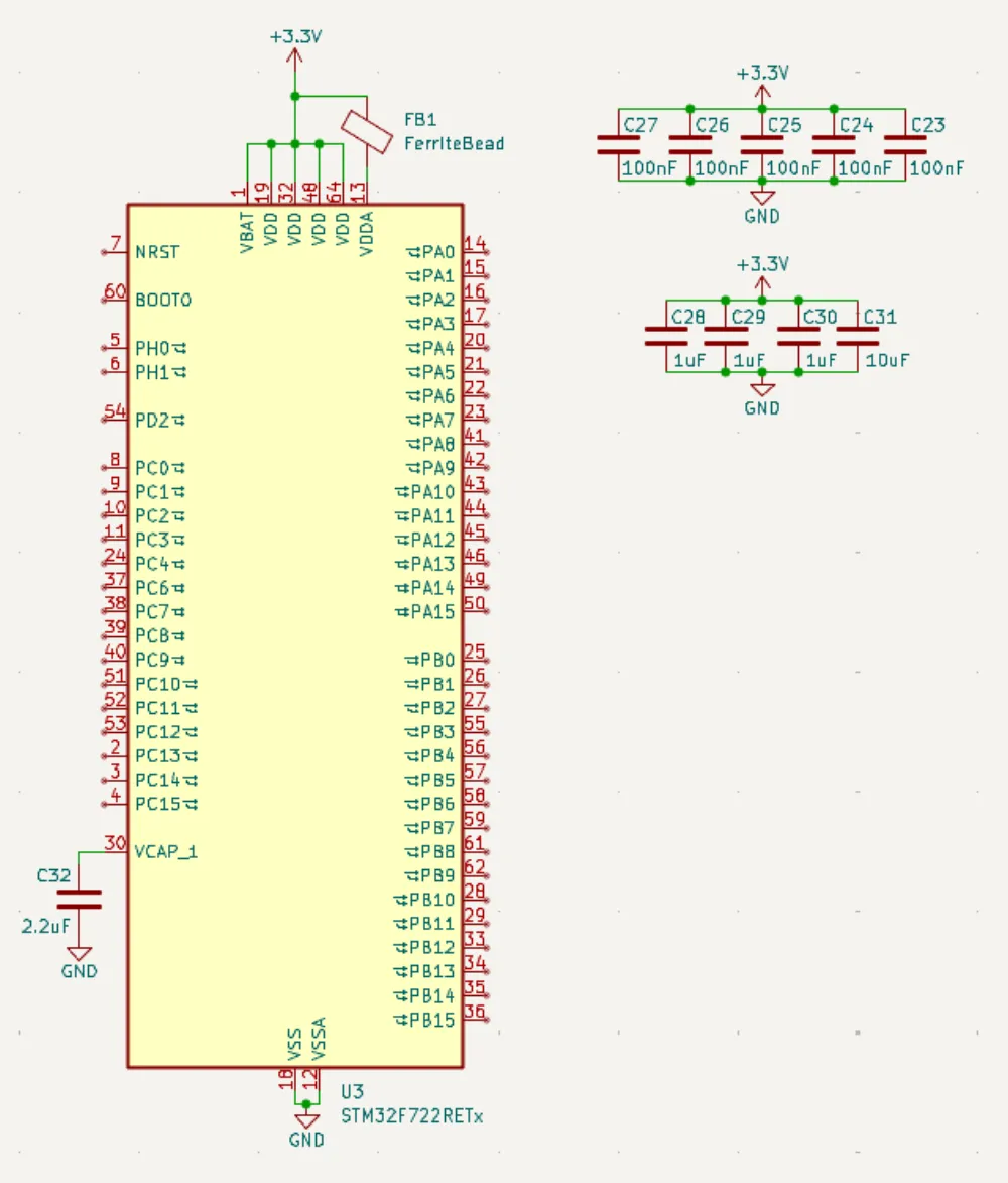
I placed the capacitors off to the side to make it look cleaner, but it's the same as if you were to connect them directly. Just make sure that when you are placing/routing them on the PCB, they are AS CLOSE AS POSSIBLE TO THE PIN THAT THEY ARE DECOUPLING OR IT DEFEATS THE PURPOSE.
Clocks
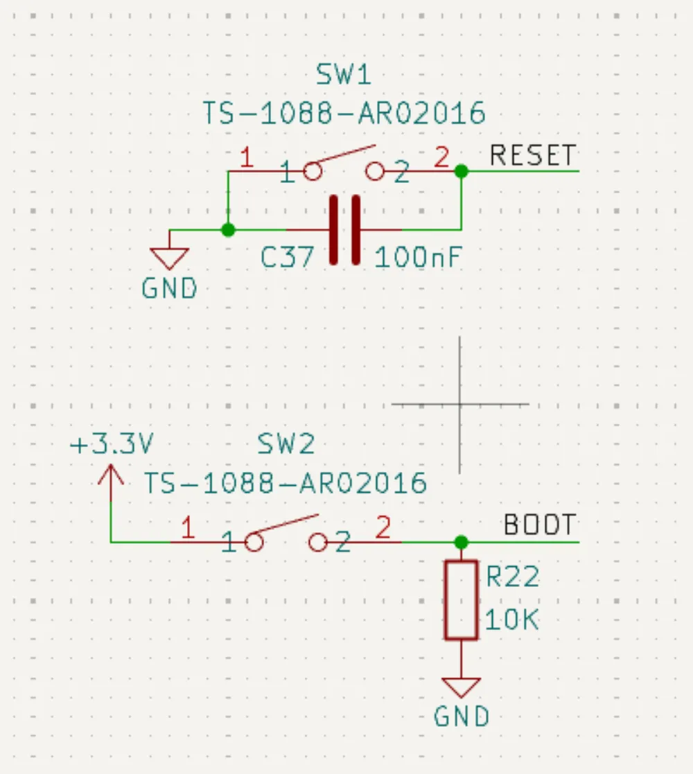
Looking at the reference design above, it shows that we need some buttons for the reset and boot pins. These buttons allow us to restart the MCU and allow it to boot into its bootloader to allow for programming through USB.
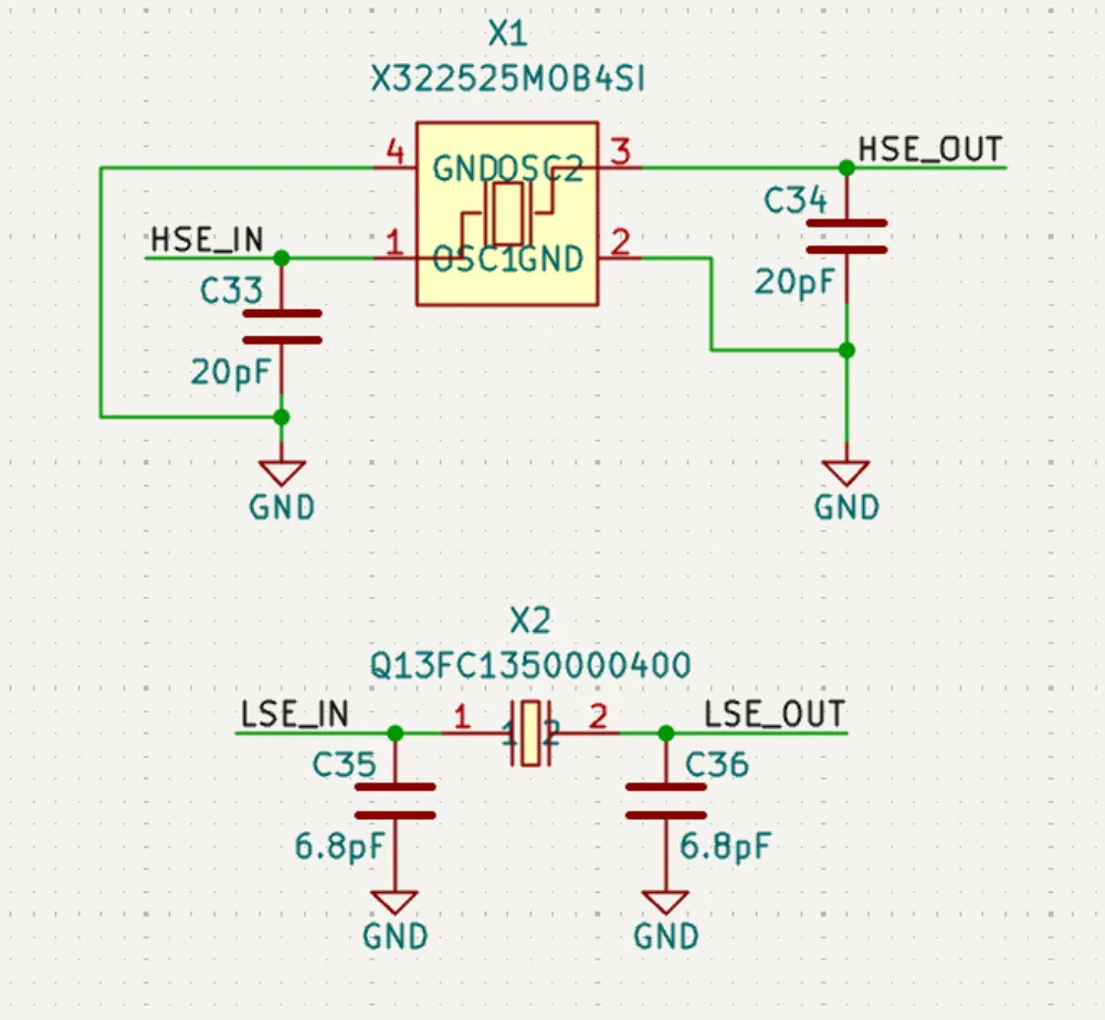
We also have to add the 32.768 kHz and 25 MHz clocks mentioned in the datasheet. These clocks are important for PWM and other functionality that requires timing that you may want to add.
I am going to import all of these parts from LCSC using the script that we used before (including the ferrite bead). Here are the updated part numbers:
- C720477 (Button)
- C9006 (25 MHz Crystal)
- C32346 (32.768 kHz Crystal)
- C141723 (Ferrite Bead)
After running the script, import all of the parts in. I replaced the ferrite bead with the part from LCSC:
Now it's time to place the crystals. These crystal oscillators use a piezoelectric (ability of certain materials to generate an electric charge when subjected to mechanical stress, and conversely, to deform when an electric field is applied to them) crystal to generate a stable and accurate frequency reference signal. When using these crystals, you need to place load capacitors:
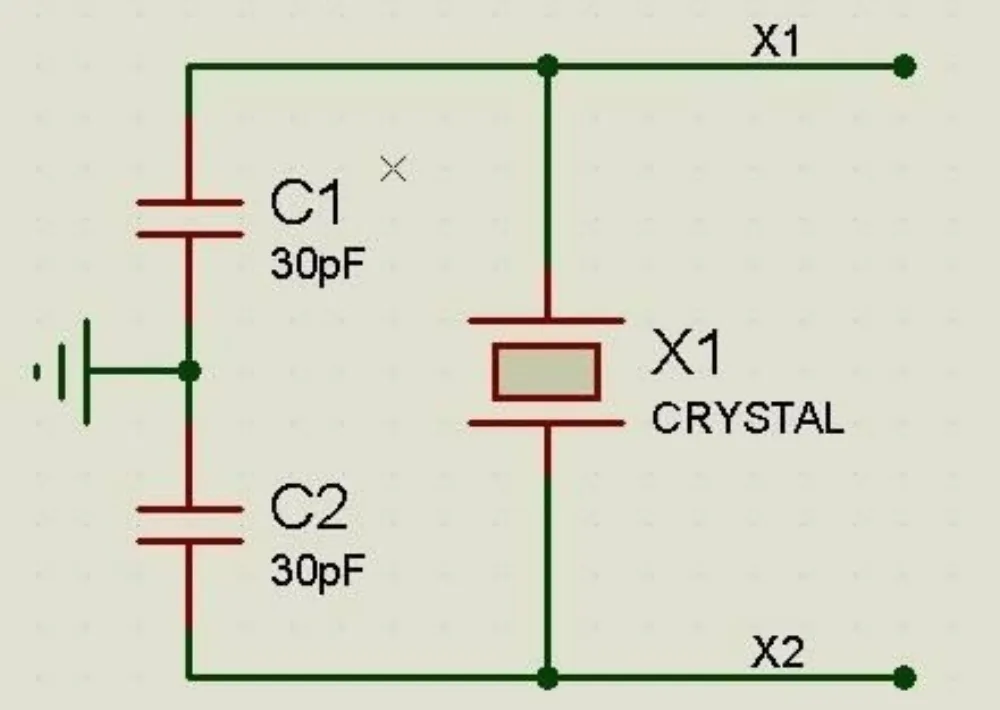
Think of the crystal like a kid on a swing. It is going back and forth at a certain oscillation. The load capacitors would be weights that you add onto the swing to speed it up or slow it down to get the exact frequency. The same applies to the crystal oscillators. The capacitors are used to fine-tune the oscillations (clock speed) of the crystal.
Each crystal has a datasheet that specifies the load capacitance that it needs, and I have already looked them up for the crystals mentioned above. REMEMBER THAT EACH CRYSTAL IS DIFFERENT EVEN IF THEY MIGHT HAVE THE SAME FREQUENCY.
The capacitors for the 25 MHz crystal should be 20 pF and for the 32 kHz should be 6.8 pF. After you're done adding them, it should look like this:
Buttons
Now for the reset and boot buttons. These are super important for flashing or working with your STM32 in general. Taking a look at the reference design above, we need to connect the reset pin to a button parallel with a capacitor to ground. For the boot pin, we need to create a button that will set the boot pin to 3.3V when we press it. (Look at the datasheet to learn more.) This allows us to change the boot configuration depending on whether the boot pin is a 1 or a 0. In the end, it should look something like this:
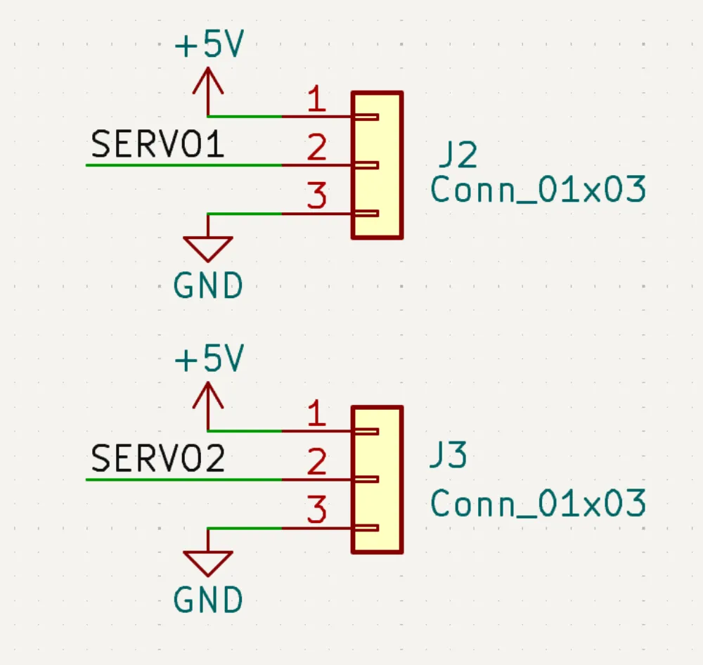
Servo Headers
Almost done, just need to add in some 3-pin headers to control the servos. They typically have a pinout of 5V - PWM - GND so it's good to keep the pinout in that same order. Mine looks like this in the end:
Finish Schematic
Now all that's left to do is to finish the schematic by adding net labels on all of the pins that we have used in STM32CubeMX. Your layout might look different from my layout if you're using a different chip or sensors, but here's how my STM32 looks after adding all of the net labels:
For the USB lines, DM = DN, and DP = DP.
For the ICM SPI lines, SDI = MOSI. (For the ICM, it's an input, so it would be MOSI (Master Out Slave In) for the STM32.) By that logic, SDO = MISO.
Note that for the I2C lines, I changed the names to be able to connect to each of the devices like so:
You may have a different pinout than me, but as long as you know which pins you are using and for what, then you'll be fine.
DOUBLE TRIPLE CHECK THAT YOUR PINS MATCH THE ONES IN STM32CUBEMX.
Now that you're done with your schematic, organize everything so that it looks nice. You might have to change the page settings via File > Page Settings in order to change the size of it:
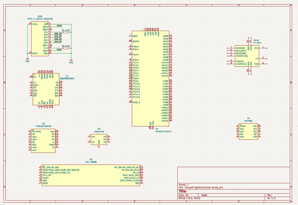
Now after organizing it a bit, your schematic should look like this:
I placed text to name each block and added a title at the bottom right.
Finally, we're done with the schematic!
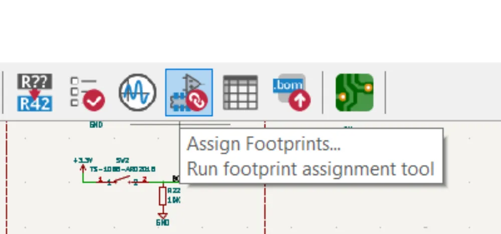
Footprint Assignment
Before continuing on to the PCB, we have to Assign Footprints which basically tells KiCad how big each component is physically and how the connections look in real life to be able to solder it.
Click on this button to open the footprint selection screen:
The lines in yellow are components whose footprints we have to assign:
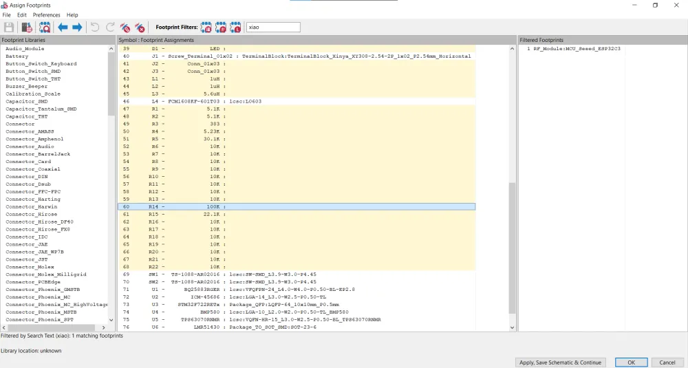
But since it's mainly resistors and capacitors, that makes it a lot easier.
Since we're designing a flight controller, this has to be as small as possible, so I am going to be choosing the smallest footprints I can (while staying within good practices). The smaller the footprint, the more it can heat up and the less it can tolerate (for resistors and capacitors). A rule of thumb that I go by is any resistors under 80K I assign a 0201 footprint, over that and it's 0402. For capacitors, any bulk capacitors (capacitors that have high values like 4.7 µF or 10 µF) I usually assign 0402. Any bigger than 10 µF and I assign 0805, but it depends on the datasheet of the component. Under the application and implementation section there is usually a table that specifies which footprints/components to use.
Now all that's left is to finish adding the footprints for these symbols:
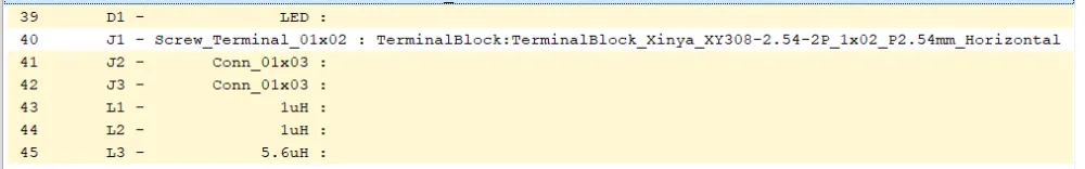
For the LED, I am going to have it in a 0402 package. And for the headers, I am going to use these footprints (basically the standard headers for jumper cables):
The inductors are a bit trickier. For this, you're gonna have to go into the datasheet and see where it says the size:
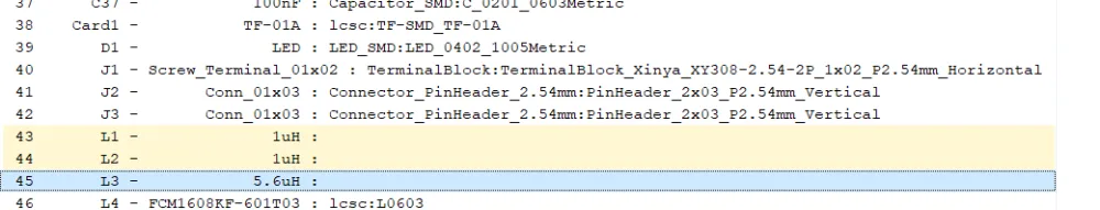
For that 5.6uH inductor, I am going to be using C18236327 (LCSC Part Number).
For the 5V buck-boost, I am going to be using C3033018. I also noticed that I had the inductor value wrong from the datasheet. THIS IS WHY DOUBLE CHECKING IS IMPORTANT:
For the final inductor in the battery charging IC, I am going to use C435392.
Press Apply, Save Schematic & Continue to save the footprints you have already placed and then import the new inductors that you have selected.
PCB Layout
Now go to the PCB section in KiCad. There's a button at the top of the schematic page that says Switch to PCB Editor to go there.
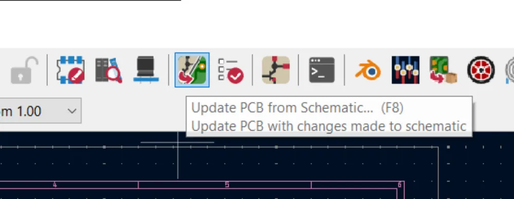
Then to import all of our components from the schematic, we hit this button:
A screen should pop up:
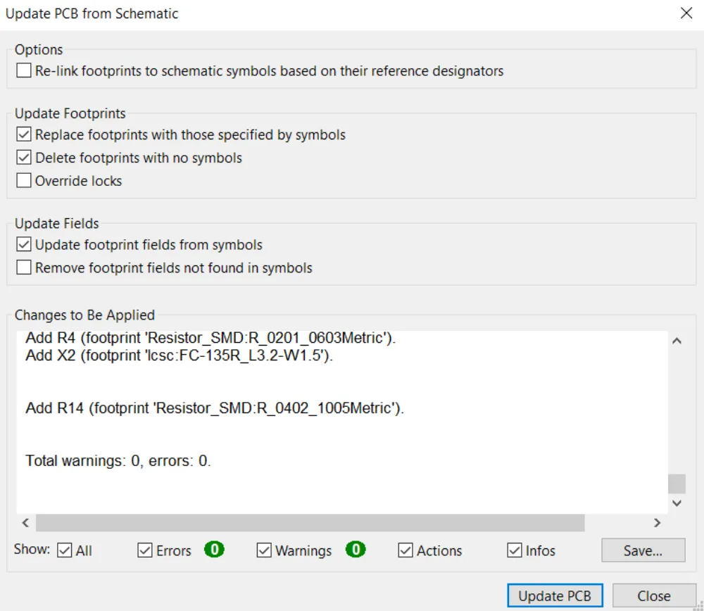
There should be no errors or warnings. Then press Update PCB to import everything from the schematic.
Now comes the fun part, part placement!
But wait, what's a PCB?
A PCB (Printed Circuit Board) is a board used to mechanically support and electrically connect electronic components. It is composed of layers of copper and a dielectric material (a material that acts as an "insulator" and isn't conductive). PCBs can have from 2-32 layers, although for this board, we will be working with 2 (maybe 4 if we need to).
In KiCad, if you look to the right, it shows the different layers:
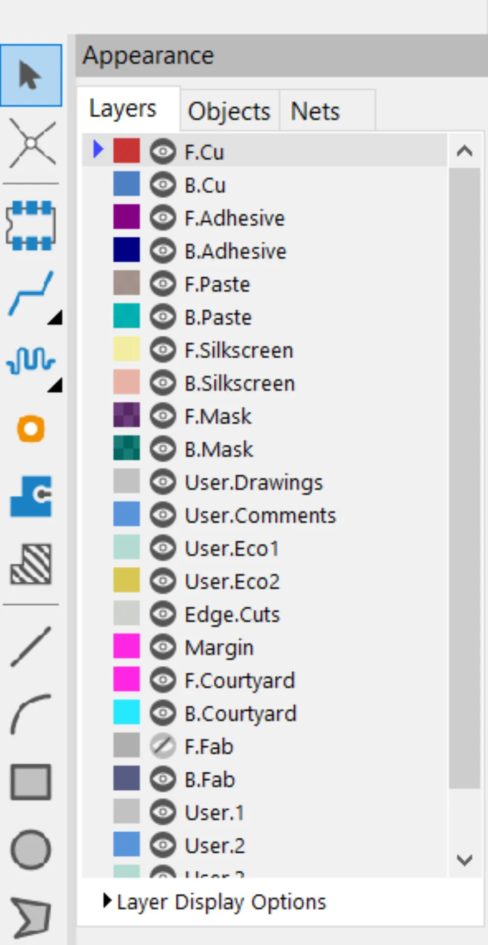
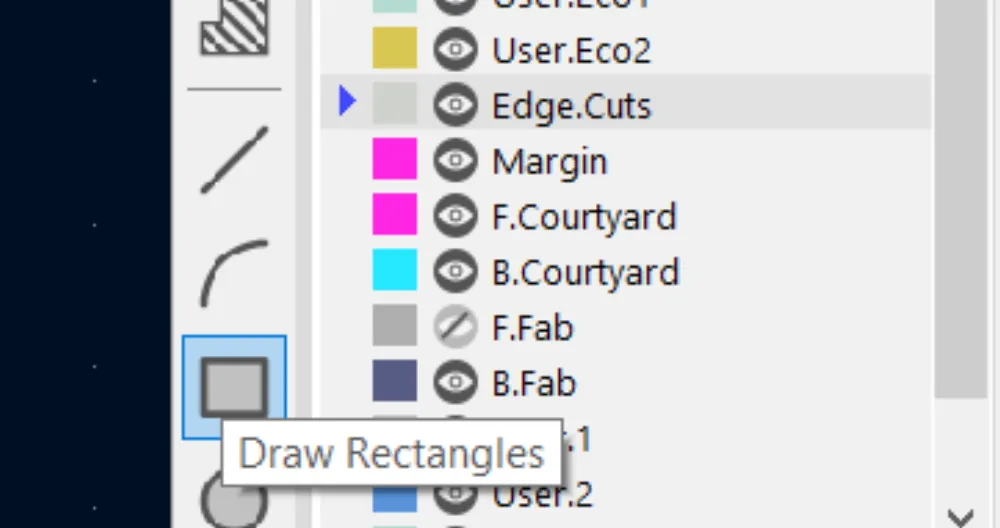
F.Cu and B.Cu (Front Copper and Back Copper) are our copper layers (denoted by the .Cu). The only other layers that are important to us are F/B.Silkscreen and Edge.Cuts. The silkscreen layers allow us to put text/images and is usually that white text that you find on any PCB. Edge.Cuts is the layer for the edges of the board (e.g., where JLCPCB will cut to make the outline). For now we will focus on the copper layers and routing. We can add more copper layers later in the board settings.
Now we have to connect each of the components and route them (create copper lines between each of them).
Layout
I personally have always relied on this one trick to route my PCBs and it has always helped me without fail. First, separate the components into their respective groups (e.g., all of the components for the battery charger, 5V regulator, 3.3V regulator, STM, etc.), then lay them out and route them in those groups, finally put the groups together on the PCB and route the connections between them.
Starting with USB-C, go to the schematic and select the USB-C section:
Then going back to the PCB editor, you should see that the connector and its parts are selected. Then drag them off to one side.
Do the same for each of the sections and after you've done that you should get something like this:
Now go section by section and place the components close to where they're supposed to be connected. Make sure to place decoupling capacitors close to the pins that they need to decouple or they won't work.
Example of the USB-C connector:
I placed the resistors close to the pins that they need to decouple and in a good orientation so that I can connect that ground pin easily.
For the 3.3V Buck converter I routed it like this:
But now I'm realizing that the components I chose are too small so I am going to make the capacitors and resistors a bit bigger:
Ignore the silkscreen for now (the yellow) we are going to come back to that later.
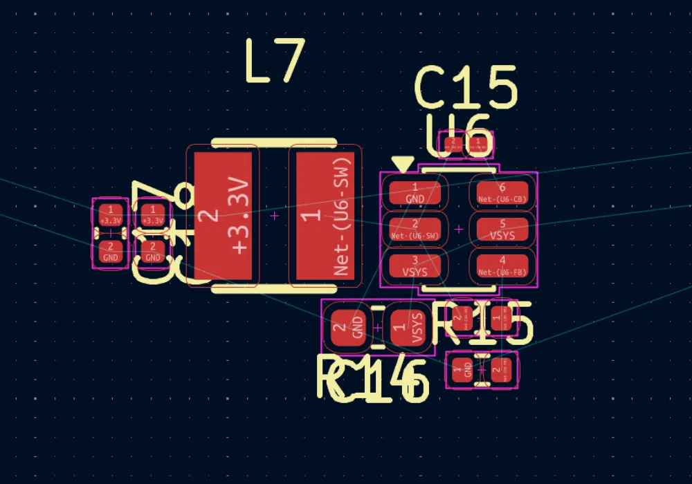
Continue on for each of the chips. For example, here is how I placed the 5V buck-boost converter:
As you can see, the capacitors are close to the pin and to each other, and all of the components I have placed in a way where I can create easy connections like so:
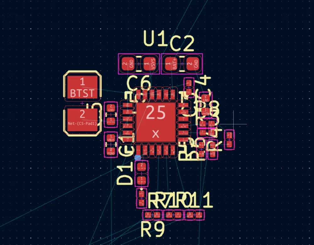
Moving on to the battery charger:
Crystals:
microSD Card:
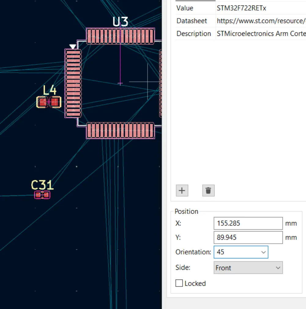
For the STM32/microcontroller, it's a personal preference of mine to rotate it 45 degrees so that it's "easier" (subjectively) to route later. You can change this by editing the orientation property:
Also for these decoupling caps:
I changed the sizes to be 0402 as they are bulk decoupling capacitors and should always be a bit bigger than the normal ones.
After laying out the decoupling capacitors for the STM32, it looks like this:
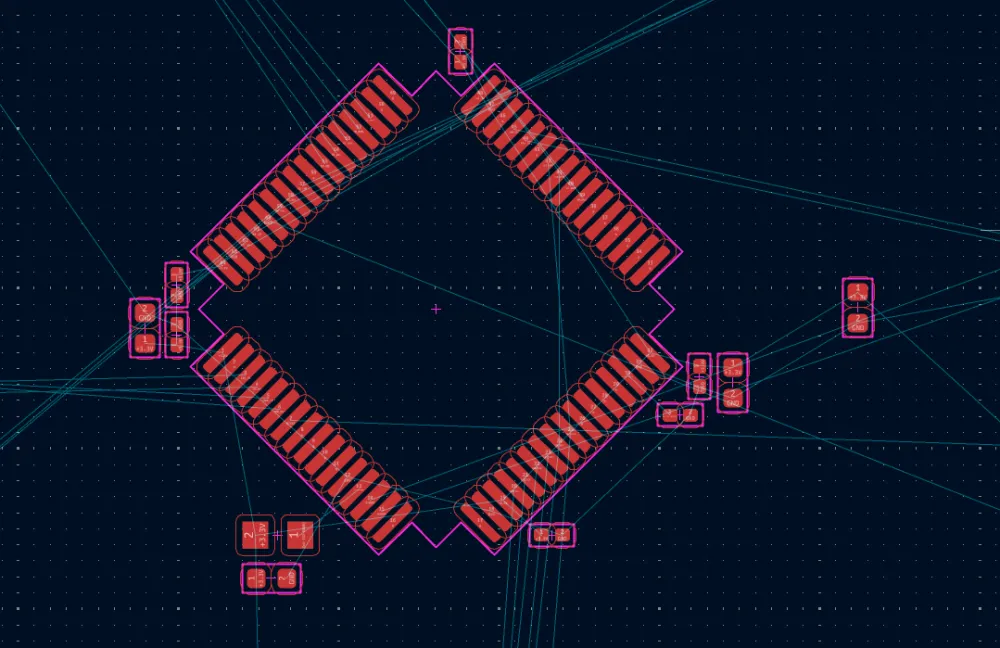
That one capacitor that is by itself on the right is the big 10 µF capacitor that I plan on laying out later depending on where the 3.3V is coming from.
Final Layout
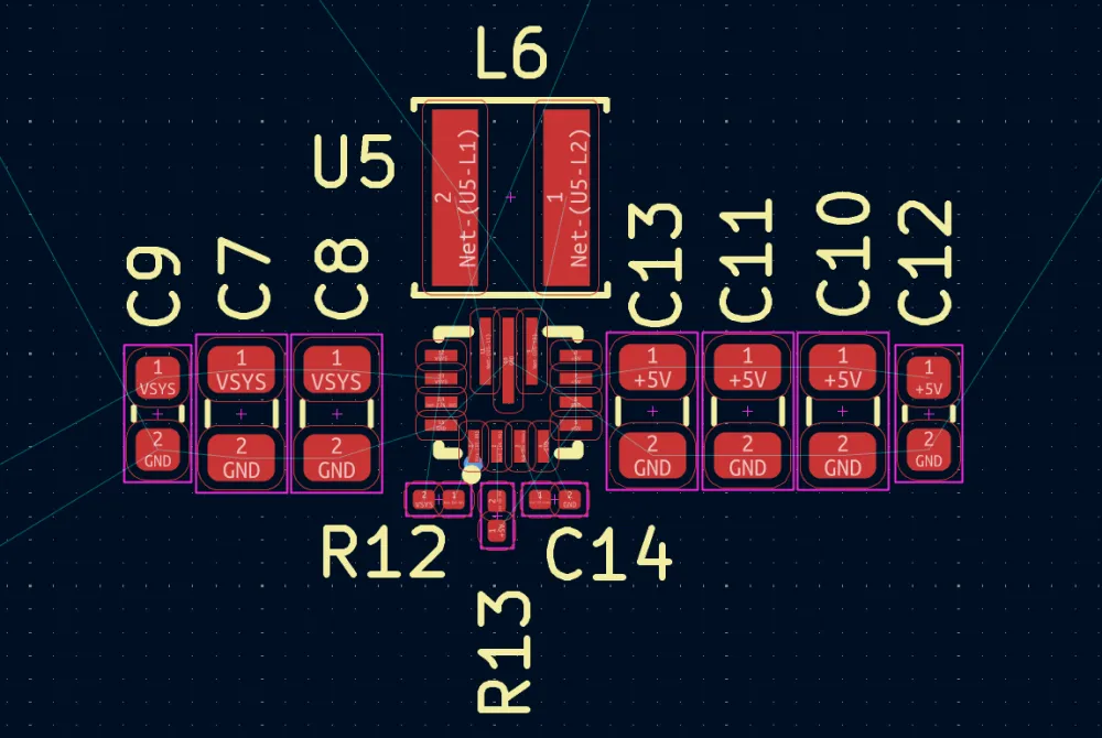
After you're done laying out all of the passive components (resistors, inductors, capacitors, etc.) and their respective ICs, it's time to layout each of those groups on the board.
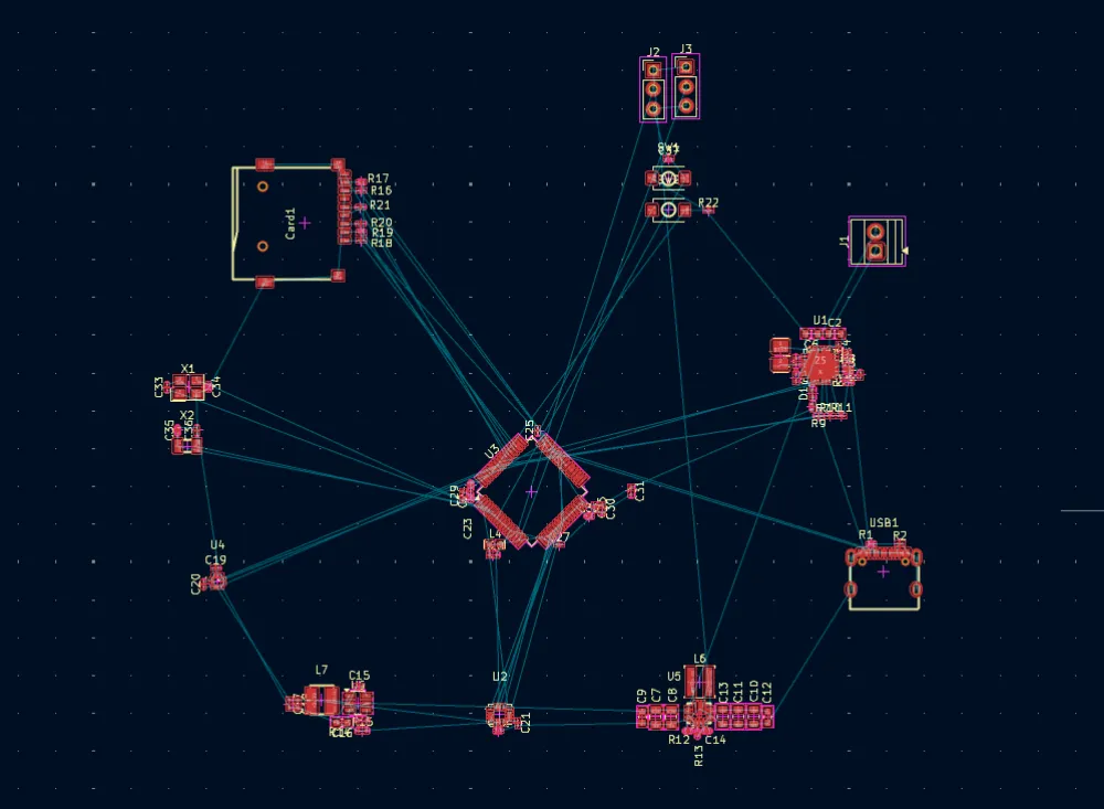
Here's what my "board" layout is and I'm going to play around with the placement of each of the groups before routing to make it more compact.
TIP
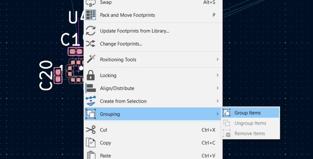
It may be helpful to literally group them in KiCad to move them around easier.
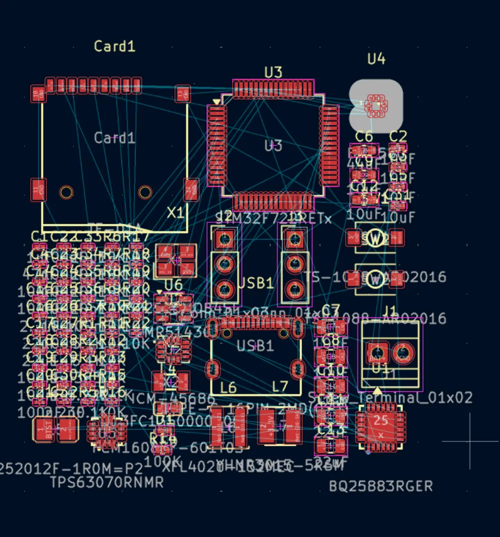
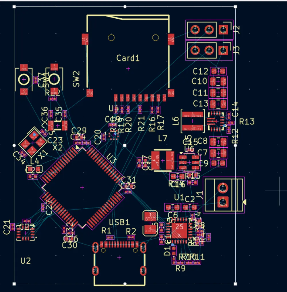
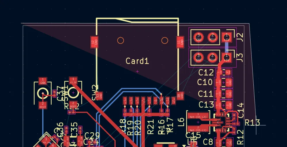
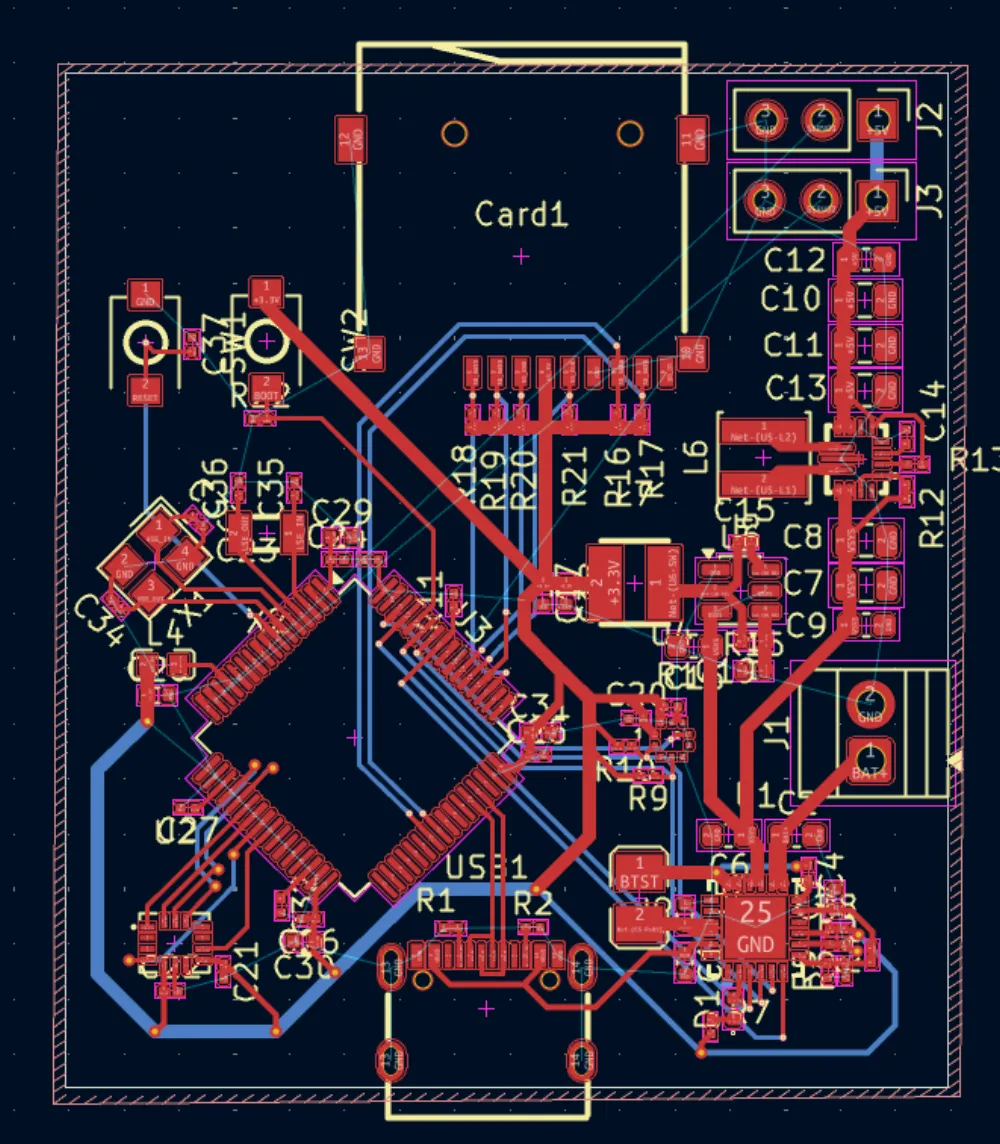
After a bit of laying out and thinking I came up with this:
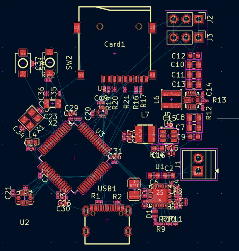
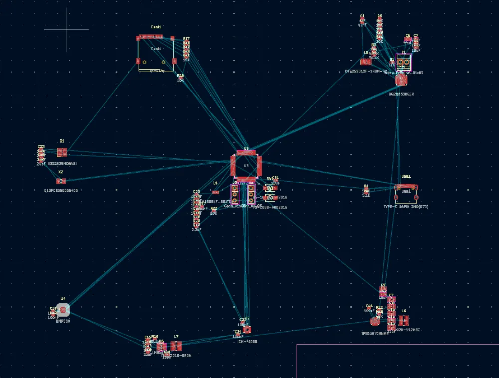
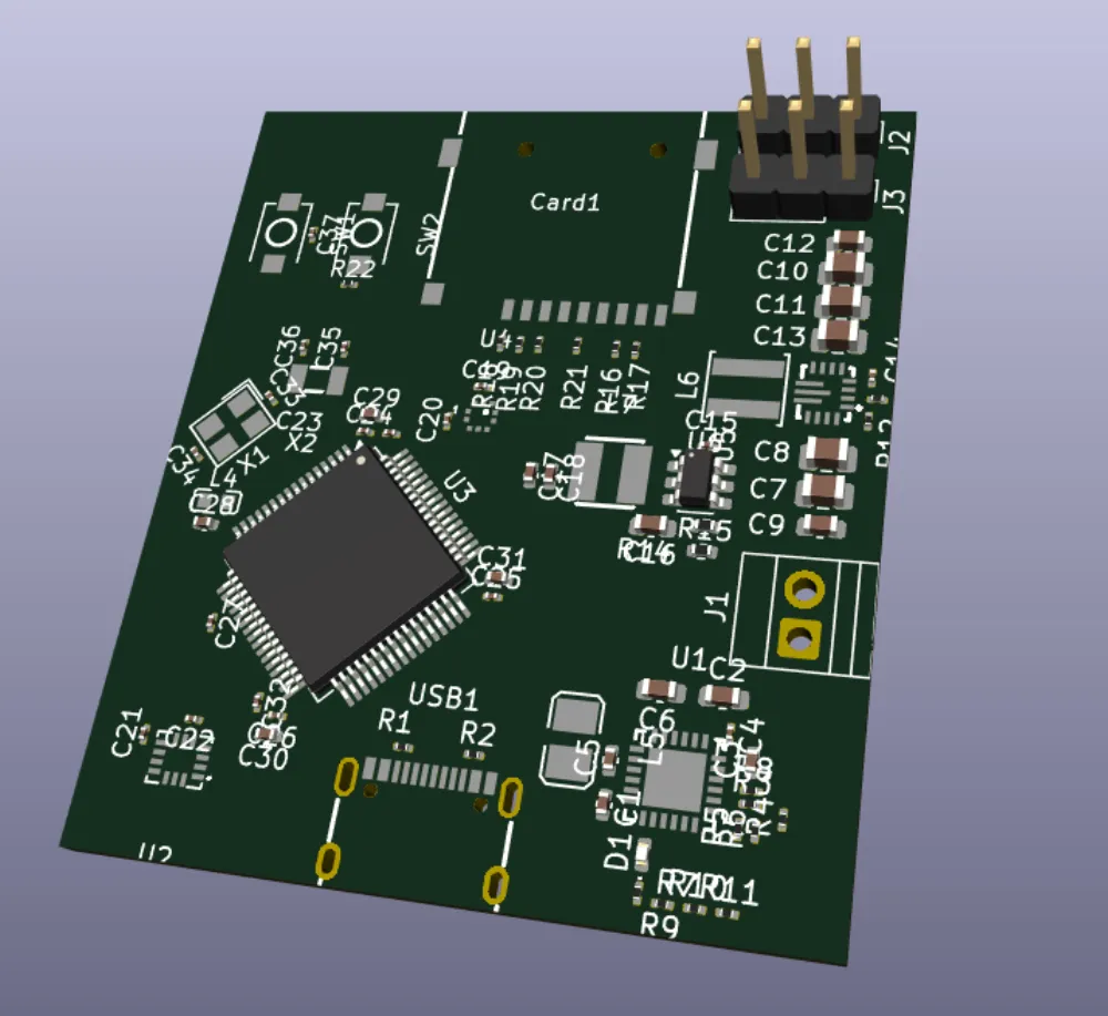
The battery charger is close to VBUS and then VSYS has an easy path through to the 3.3V buck converter and 5V buck-boost. The battery connector is also on that side. On the top is the microSD card with a connection to the STM32 directly under it. On the top left are the buttons for boot and reset and also the 2 clocks. On the bottom left is the IMU that is kept separated from the rest to reduce noise (happened by accident lol) and the STM32 in the middle whose USB DP and DN pins are inline with the USB-C port.
You don't have to use this exact layout but try to have one that's "organized".
Now after defining the layout, go to the Edge.Cuts layer and create a rectangle with the tool on the side:
This will be the PCB outline.

When I originally created the board size to cover all of the parts, it had a size of 42.7mm x 47.8 mm so I decided to round it to 40mm x 46mm (optional). After creating the board outline, you may need to shuffle some stuff around for it to fit. It's good practice to put the USB-C connector hanging out a bit so that you have space to plug in the cable like so:
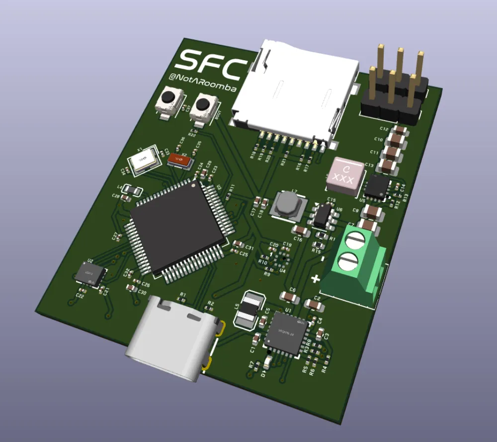
After organizing it, look at the board in the 3D viewer to get a good feel for how the components are going to look. Don't worry if the silkscreen/3D models look terrible for now, we will fix that at the end.
Routing
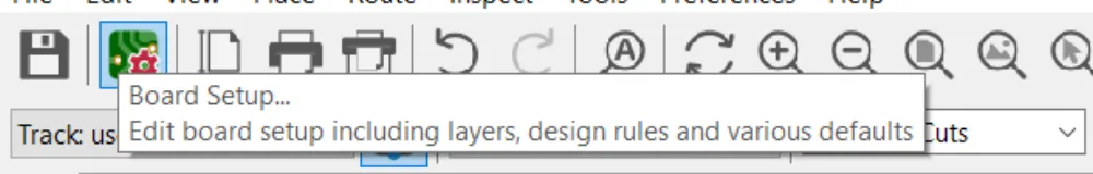
Before we start routing, let's configure the Design Rules. These are rules that KiCad has to impose certain restrictions like spacing between components and track width and via size, among other things. It is also where we can add default sizes for vias (holes that connect tracks between layers) and tracks (copper lines that connect components).
Go to the Pre-defined Sizes section:
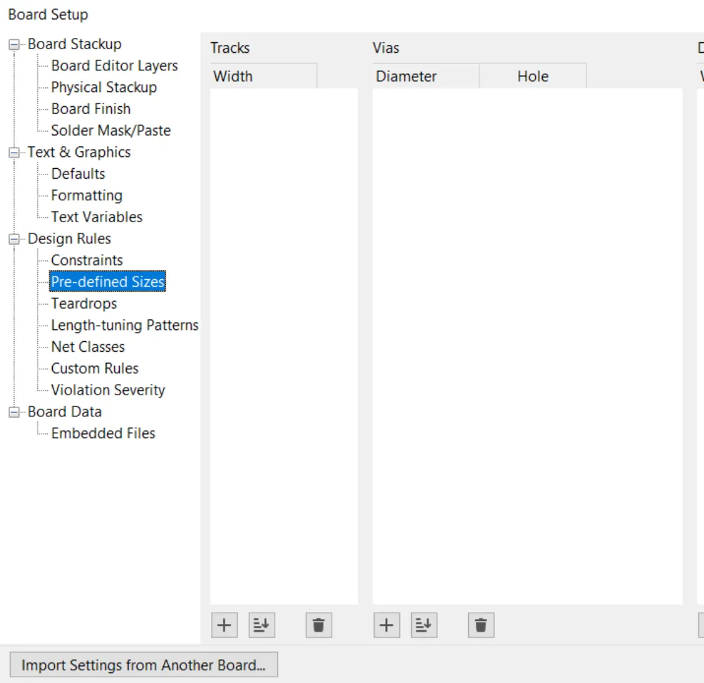
I am going to add 0.6mm, 0.4mm and 0.2mm track widths. For vias, I usually go with vias that have 0.6mm Diameter / 0.3mm Hole and 0.4 Diameter / 0.2mm Hole.
Now after that we have to edit the constraints of the board so that KiCad doesn't throw an error when we try to place them. Go to the Board Setup and then Constraints.
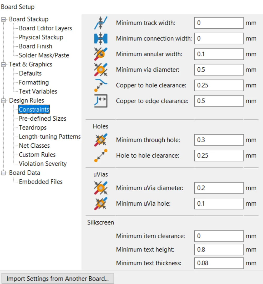
Here we are going to change a couple of settings due to the size of our board. We need to be able to place smaller vias and traces, so change the Minimum via diameter to 0.4mm and the Minimum through hole to 0.2mm. After that's done, click OK and you can start routing!
How to Route
Basically connect each of the pads to their connections and try to use as few vias as possible. I usually try to route the signal stuff (USB, sensors, microSD, crystals, etc.) first and then the power.
(Press x to start routing or use the buttons on the side).
Starting with the USB-C data lines, these are what's known as a differential pair, so they have to be the same length as they carry a signal that needs to be in sync with the other and the only way for that to happen is if they're the same length. Start connecting them like so:
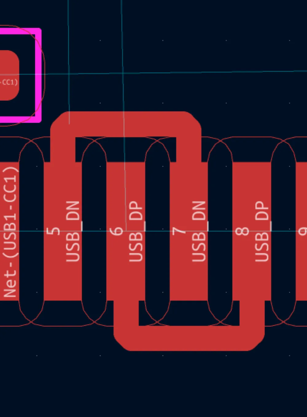
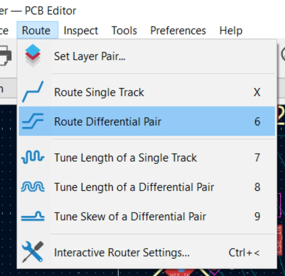
Then go to Route > Route Differential Pair
and then click on the USB_DP to the far right:
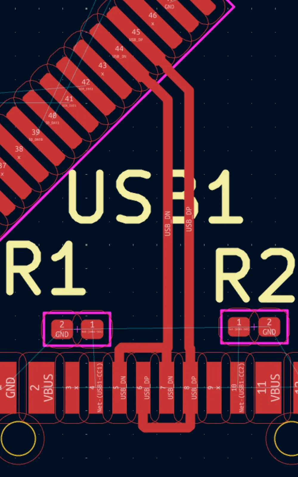
Then route it to the STM32. That's basically the only component that needs differential routing.
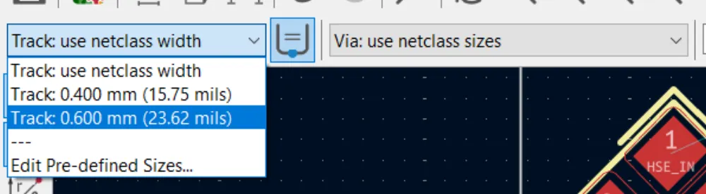
Moving on, just some general tips. I personally like to use 0.6mm or 0.4mm width for power stuff, mainly anything that runs either 5V (0.6mm) or 3.3V (0.4mm), and you can change the track width or via size from these drop downs at the top.
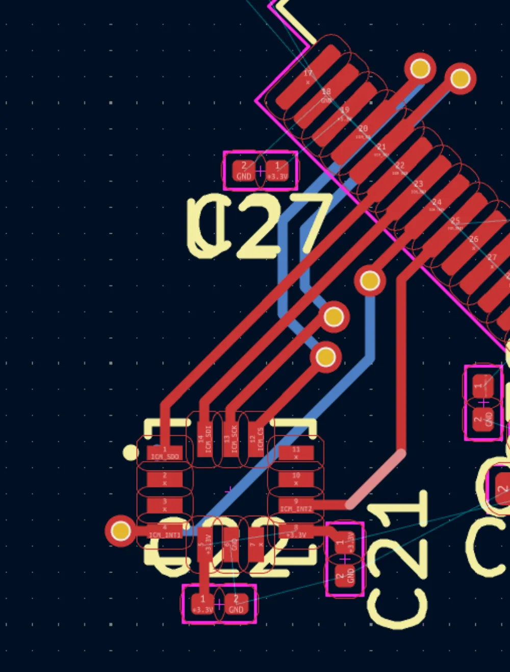
I also like to do the same as in the layout where I route all of the passive components to their respective ICs before then routing those groups together. For example, routing the decoupling capacitors to the IMU before connecting it to the STM32:
You might have to rotate components as well to get a good placement. For vias, I aim to use a maximum of 2 per line like so:
Don't worry about connecting the GNDs for now, as we are going to use what's called a ground plane (a copper area of GND that can connect to pins/pads).
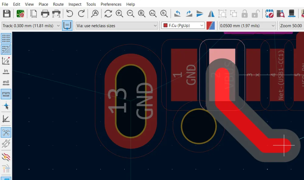
Sometimes for VBUS on USB-C or any other component, you might have vias that can't pass through, so I added a 0.3mm track width in the board settings and it works:
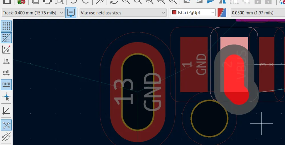
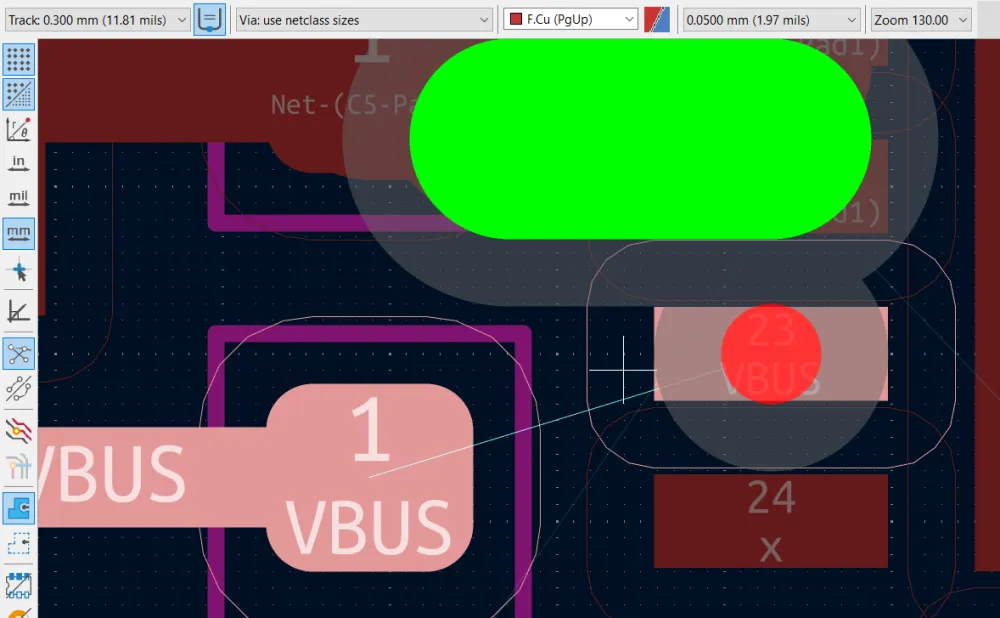
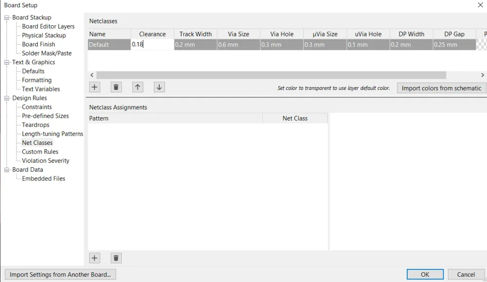
If KiCad doesn't let you place a via on a pad for whatever reason, you can edit the clearance in Board Setup > Net Classes. I set it to 0.15, but try not to set it any lower as the minimum for JLCPCB is 0.1mm:
This is how I routed the Battery charger:
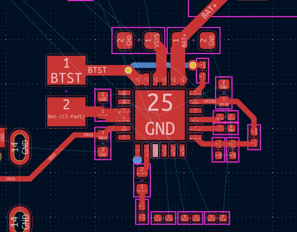
See how I used wider traces for power lines and thinner traces for the other pins. I plan on wiring the I2C lines and INT pins connecting to the BMP580 like so:
I connected them to the STM32 through the underside to save space (very useful sometimes). Also, I hid the silkscreen layer so that I can route easier.
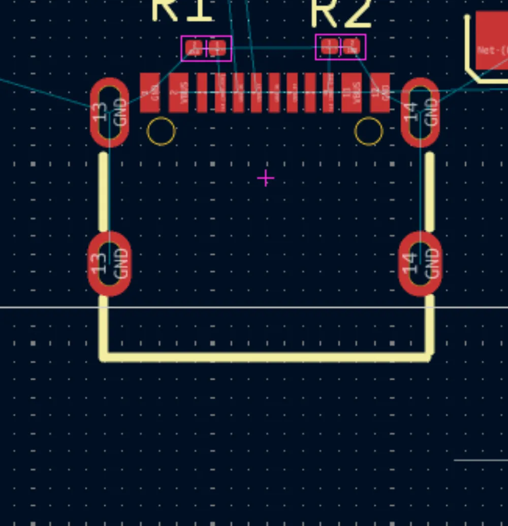
Then routed the microSD card:
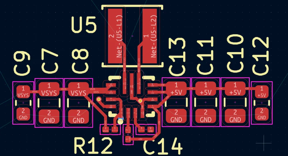
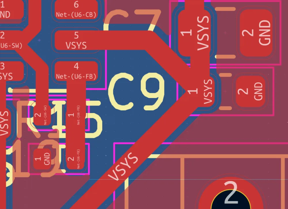
Then finally I routed the 3.3V line, using 0.6mm tracks and then branching off into smaller 0.3mm tracks to connect to the different ICs.
REMEMBER THAT THE 3.3V MUST GO THROUGH THE DECOUPLING CAPACITORS FIRST BEFORE REACHING THE PIN LIKE SO:
After routing your board should look something like this:
Now we are going to add the ground pours. This is so that we don't have to manually connect all of the ground pads and it also helps with interference and noise across the board.
Go to the right and click on Draw filled zones and click on one corner and a window should pop up:
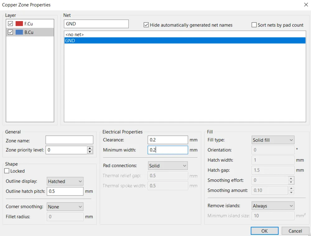
Here you need to select both layers of copper and select the GND net. Then you need to change the clearance and minimum width to both 0.2mm and also change the Pad connection to Solid or Thermal reliefs. Solid allows the ground plane to connect to the pads better but Thermal reliefs is good if you need to solder/fix the board as the solid ground plane makes it difficult to heat up specific components. For this tutorial I am going to use Solid but feel free to use Thermal reliefs if you want to be able to solder it later. Press OK and start creating the zone like so:
You want it to look something like this:
Then press b on your keyboard and it should fill the zone automatically (Ctrl-b to clear them).
Now you should check if you have any ratlines (blue lines that signal unconnected pins) and fix them. In my case, I forgot to connect the servos so I will do that now.
Now you need to check if there are any holes that don't have any ground plane and add a stitching via (via that connects ground/power planes to cover everything) like so:
You also might see a ratline connecting a piece of the ground plane. This usually means that you need a stitching via in that area.
As you can see, the ground plane connecting to Pin 18 isn't connected to the rest of the ground plane, so we need to add a stitching via there like so:
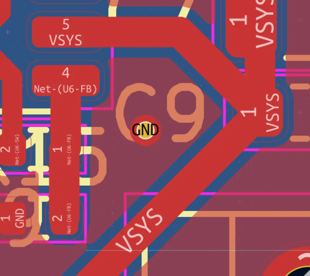
SUPER IMPORTANT: FOR ANY COMPONENTS THAT HAVE A THERMAL PAD, CONNECT IT TO GND WITH A STITCHING VIA (depends on the chip but check the datasheet to be sure):
(You can edit the properties by right clicking the pad and editing the Net name.)
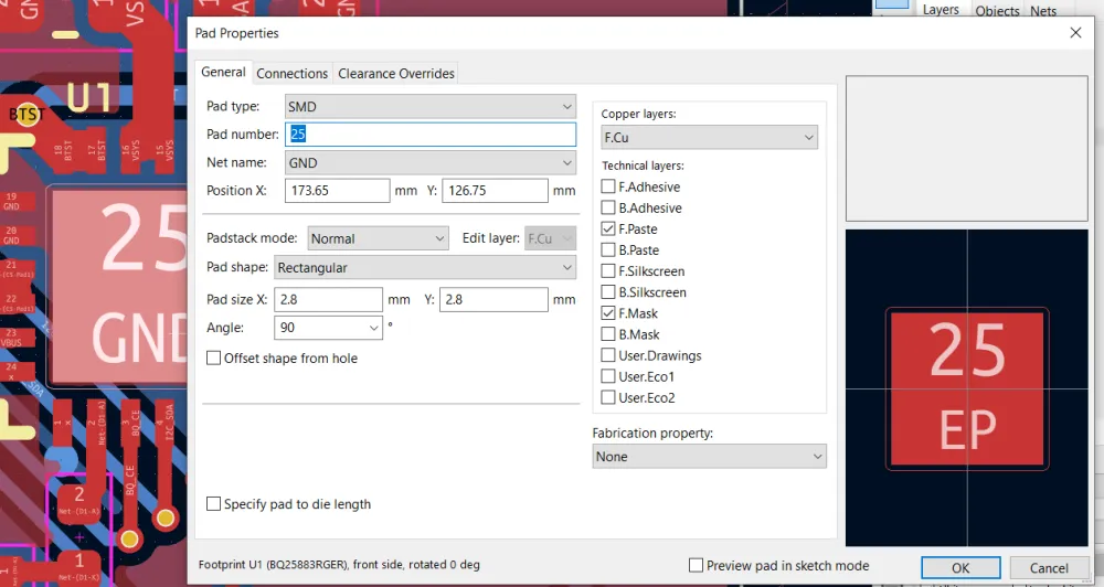
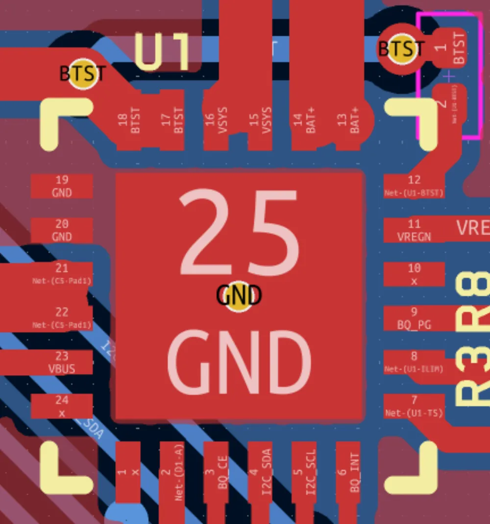
Also Notice how I didn't connect the grounds together and connected both PGND and GND, that was made automatically by KiCad when I connected the EP Pin of the battery charger:
After connecting everything we are going to run Check DRC which basically checks the design rules and makes sure our board is ready for production.
Then click on Run DRC:
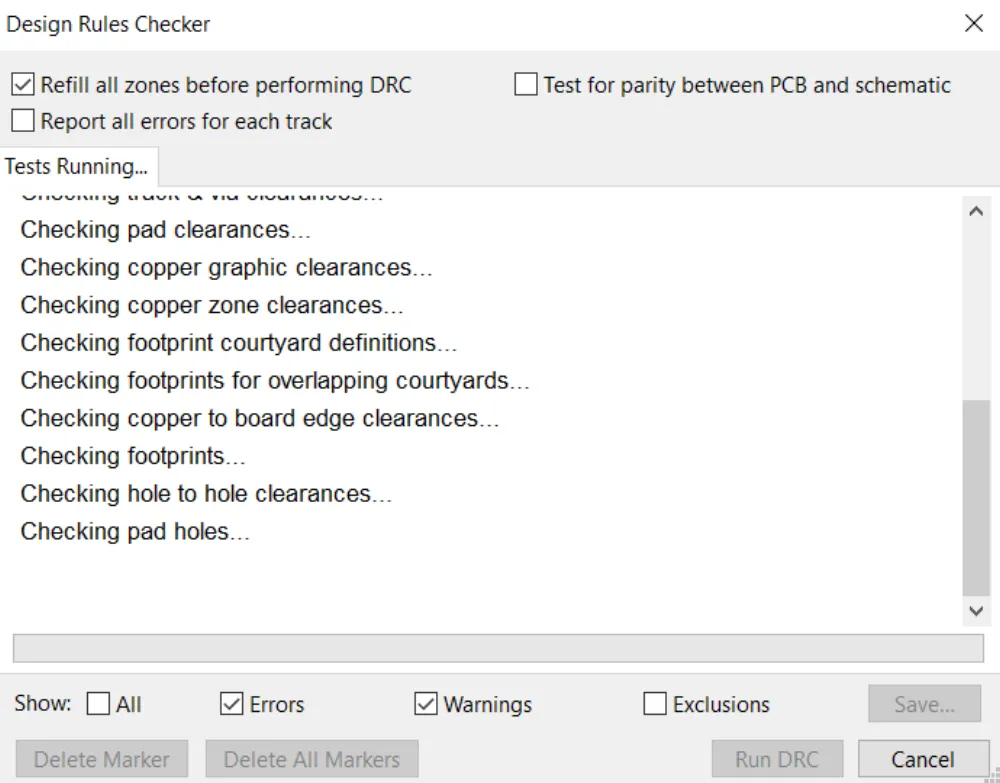
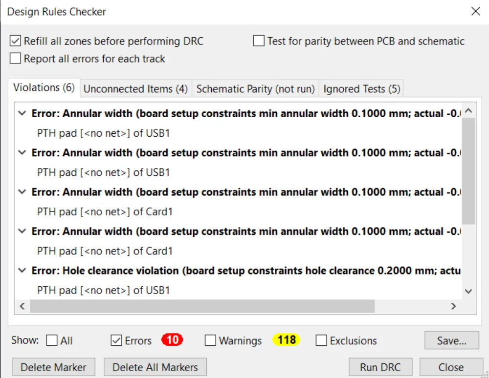
Unselect the warnings and look at the errors. If there are any errors about unconnected pads then you should probably go back and make sure that everything is connected. There are some errors but those are from the parts that we imported like the USB-C and microSD card that KiCad is complaining about the holes:
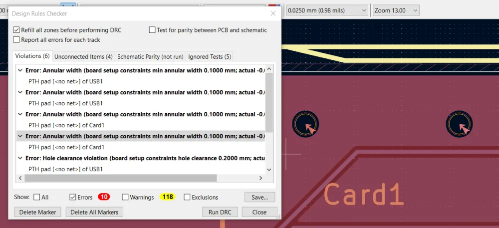
Those errors are safe to ignore but any others you should probably fix.
And with that out of the way, congrats! You've finished the PCB!
Now all that's left is to add silkscreen and make it look pretty and then get the files ready so you can order it on JLCPCB (or any other board manufacturer).
Finishing Touches
Now I'm going to fix the silkscreen component names so that they look better (and a bit smaller). Go to Edit > Text & Graphics Properties
This window should show up:
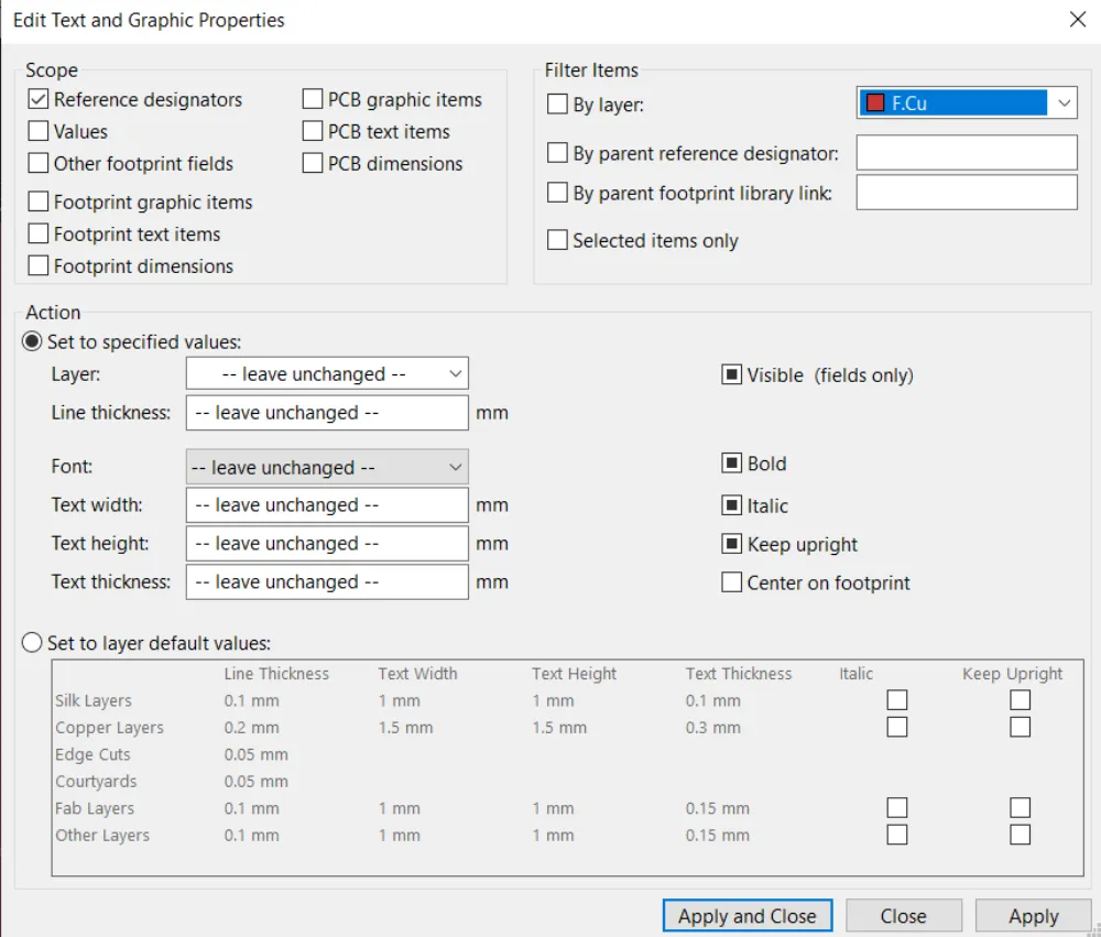
Here you're going to select Reference designators as this will select all of the designators (R1, C1, etc...) on the board so we can edit their properties. Then in the action I am going to change the font and the size:
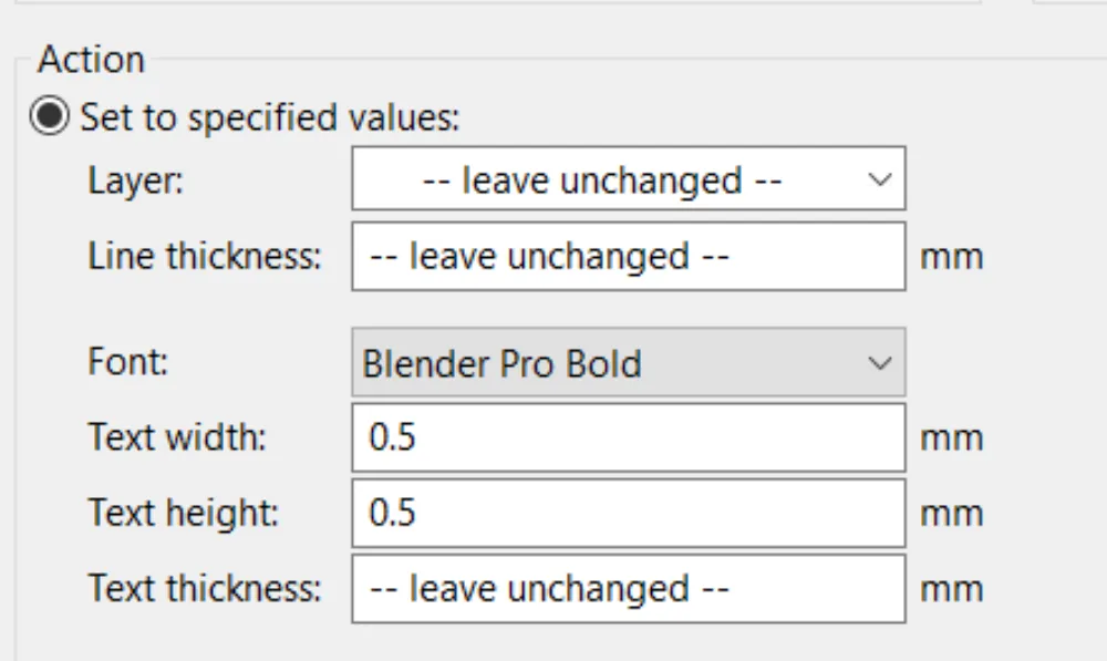
You can set these values to whatever you want but I am going to go with this. Then click Apply to test it out and Apply and Close when you are done.
Now all I'm going to do is organize the references like this:
(before)
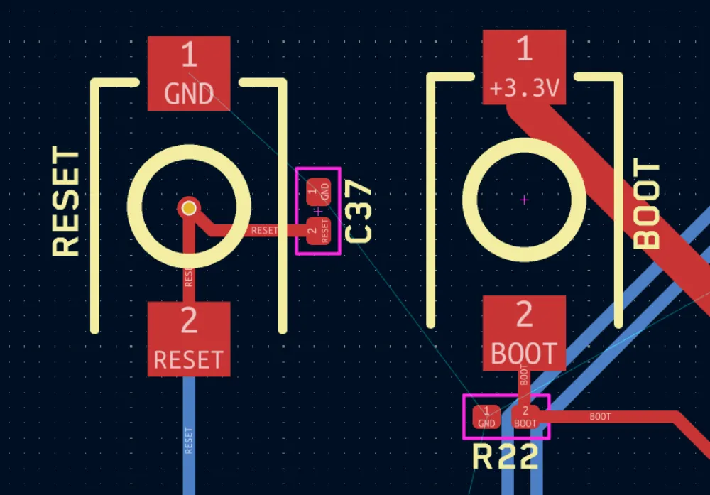
(after)
This is completely optional but look at how neat it looks now with all the designators/references properly sized and placed:
I even added text to the battery connector to show which side is + and -.
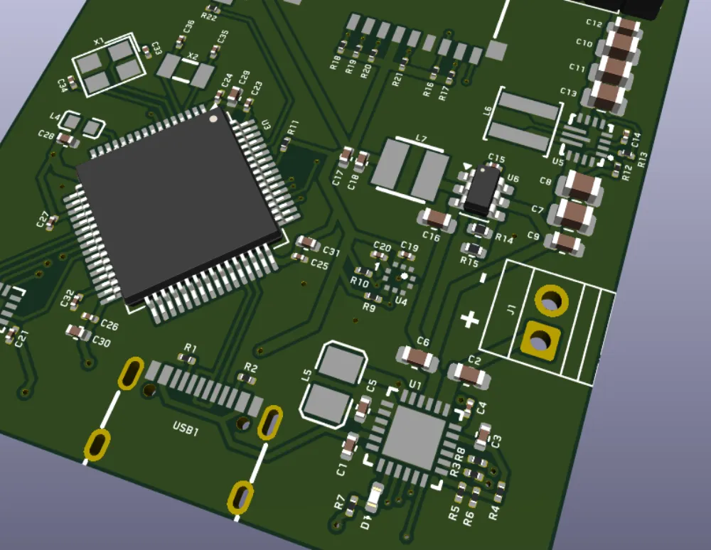
If you want to add the 3D models to render, then just go to properties and find a 3D model that works for you:
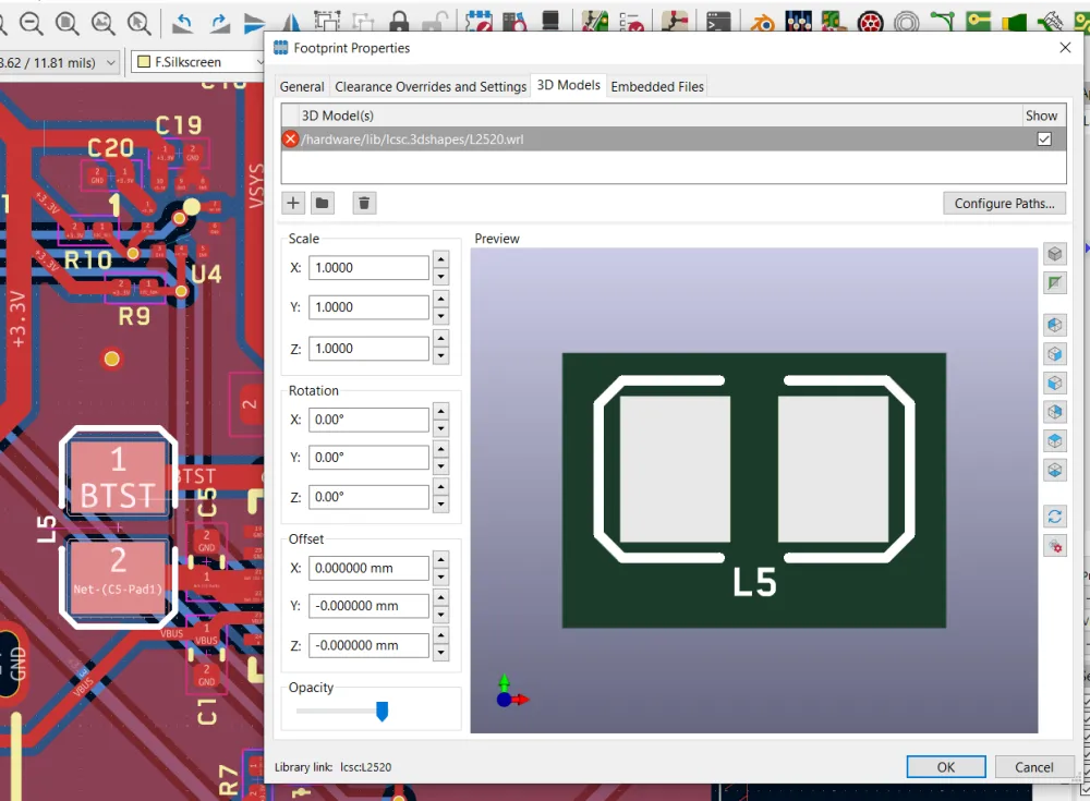
(You may have to click on the folder icon next to the path/show button to change the 3D model from a .wrl to the .step in the same folder for imported LCSC parts for it to show. Just changing the name will not update it.)
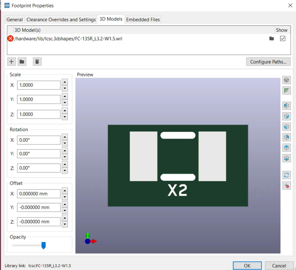
(Before)
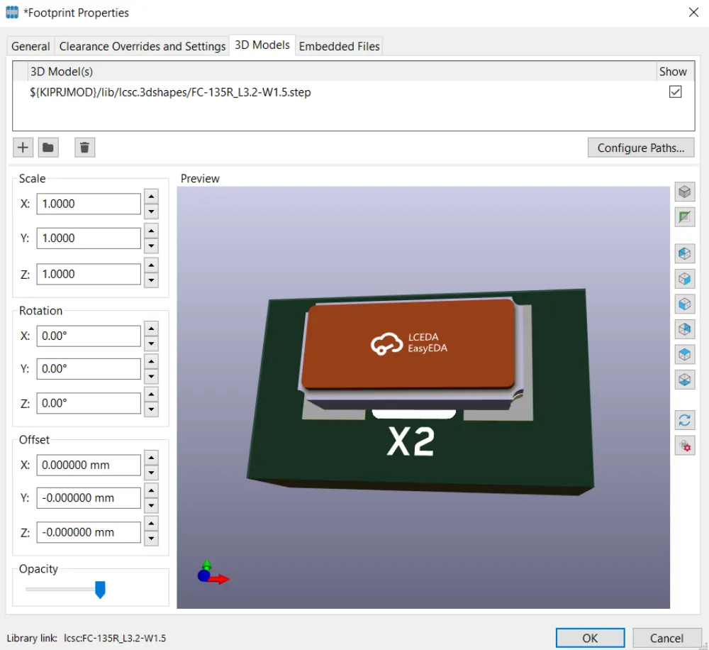
(After)
And you're done!
Exporting Production Files
To get your project ready for submission, we need to export the production files (gerbers, etc.). These files tell JLCPCB or whatever board manufacturer how to make the board and which components to place.
![]()
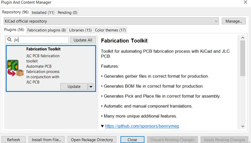
Thankfully, there's a plugin that KiCad has to make this export easy. Go to the Plugin and Content Manager in KiCad and search for jlc.
You should see this plugin show up:
Press the install button and then Apply Pending Changes to install it. Finally, go back to your PCB screen and you should see this icon:
![]()
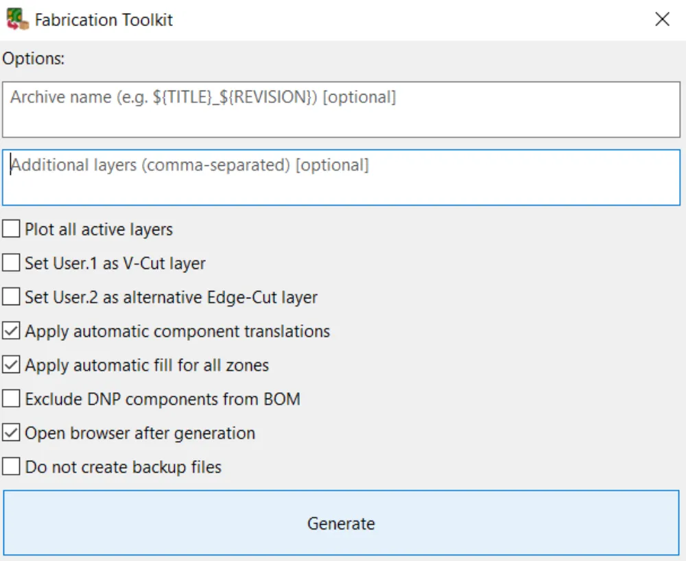
A window should open and click Generate:
It should create this directory in the hardware folder:
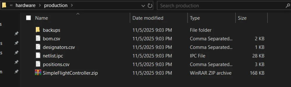
But I'm going to copy it out of that folder and move it to the root so that reviewing is much easier.
Now open JLCPCB and upload the gerbers (ZIP file that has the name of the KiCad project) in the production folder to see how much it costs.
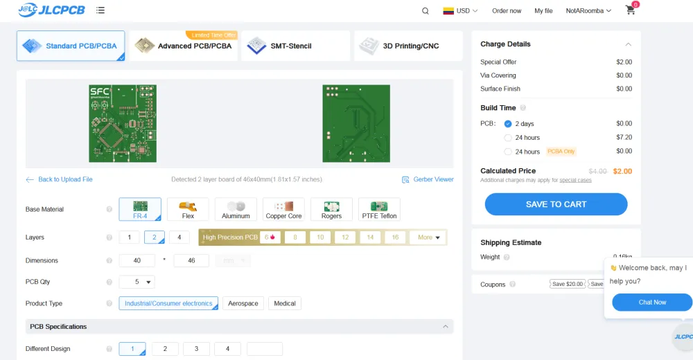
Select PCBA and make sure that it is only one side and that you order 2 and not 5 boards assembled to minimize cost:
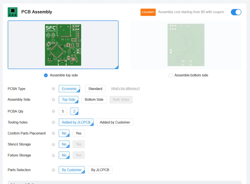
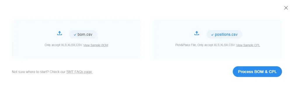
Continue and upload the BOM and CPL (BOM = bom.csv, basically the components and their ID; CPL = positions.csv, where exactly the components are placed):
Depending on the sensors you use, you may have to use standard PCBA:

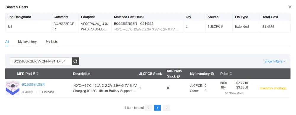
If there are any components that have shortfall, then you need to order them separately and add them to your library before ordering:
Continue without placing the parts for now to get the general cost of the board:
CONGRATS! YOU'VE MADE YOUR FIRST FLIGHT CONTROLLER!
Feel free to modify this board to include more sensors, servos, peripherals, microSD cards (lmao), literally anything you can put your mind to.
Firmware
Now you can either write your firmware through STM32CubeMX/VSCode or use STM32duino.
STM32CubeMX
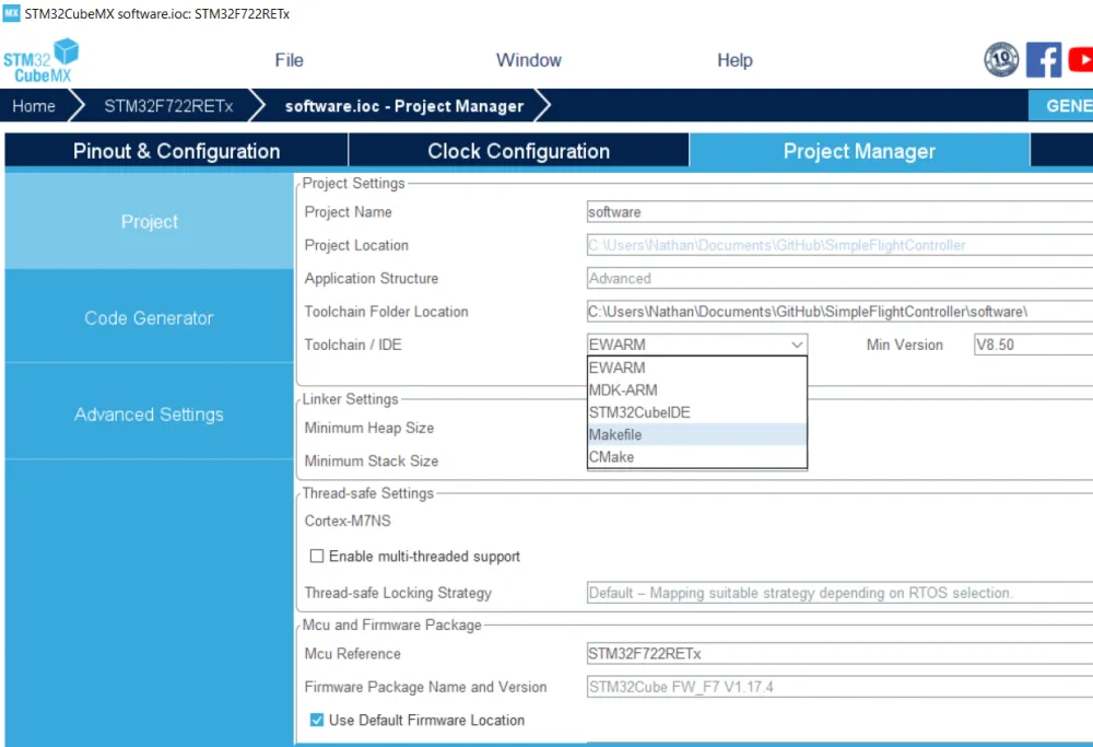
After you have received your board, you need to write the firmware to communicate with the STM32. From STM32CubeMX, go to the Project Manager section, then click on Toolchain / IDE and select Makefile. This allows you to use VSCode or any other code editor to edit the files much more easily without having to use ST's software.
Now click the Generate Code button at the top and download/install any packages that are required.
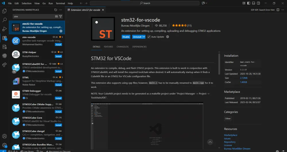
After that's done, open VSCode and open the software directory. You're also going to want to install this extension to make building the software much easier:
Then you should see this button on the side:
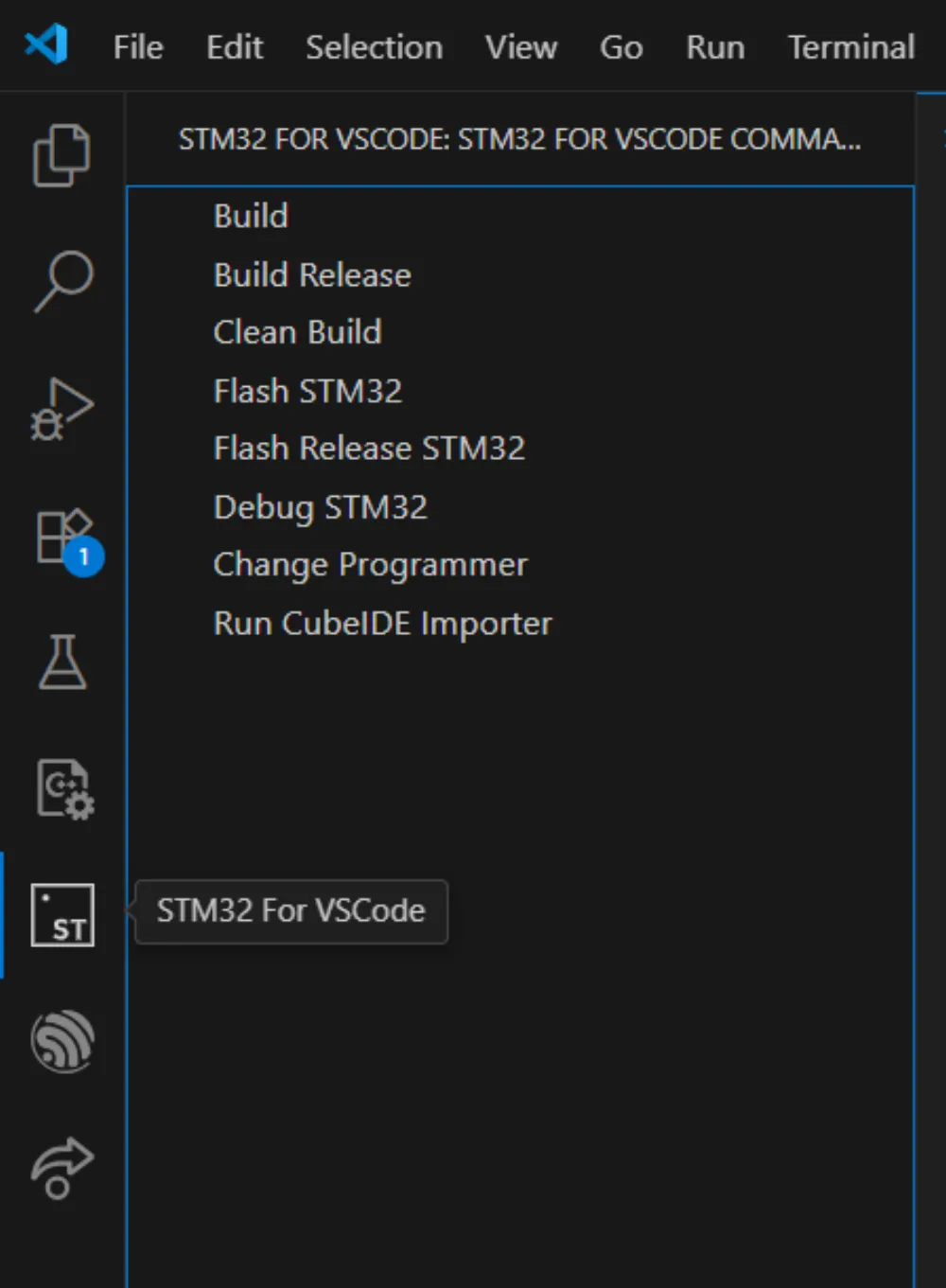
This will allow you to build and flash your flight controller all from VSCode!
If you need to edit the pinout or functions of any pin, remember to generate the code again from STM32CubeMX.
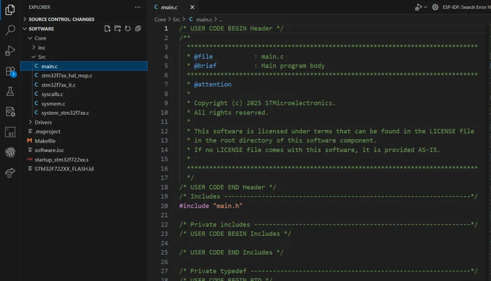
Edit main.c and remember to keep your code inside the commented sections that say USER CODE BEGIN and USER CODE END to prevent it from being overwritten when you generate the code again. There are many tutorials online/on YouTube on how to program with STM32, so I'd recommend looking there. You will also need files called drivers to control each of the chips/sensors that you use, but those can be found on the internet/GitHub and can be imported into your project easily. (example)
STM32duino
Follow the instructions in the GitHub
If you have any questions feel free to DM me on Slack (@NotARoomba) and if you want to check out my other projects, here's my GitHub / Website.