Make a LoRa Puck!
note: this guide assumes some previous knowledge about KiCAD / basic electronics!
How does your smartphone send and receive signals? How can a car receive broadcasts? How does GPS work? Well, they answer to all these questions lies in one word: RADIO! Radio lies on the high-frequency end of the electromagnetic spectrum. The radio spectrum encompasses systems like amateur radio, satellite systems, and FM radio stations, each having their own frequency. In this guide, we'll learn how to leverage one section of frequencies, called the ISM Band, to send and receive our own signals.
There are two main ISM bands:
- 915MHz - United States
- 868MHz - Most European countries Be sure to check your local regulation for license-free ISM band use. This guide is primarily built for 915MHz, but much of the same hardware should work.
The final product will be a 4-layer board with an SX1262 radio module, an RP2040 microcontroller, and pins broken out for development.
Table of Contents
- Setting Up a Project
- Fleshing Out the Schematic
- The SX1262
- Footprints
- Layout
- Routing
- Guidelines for Routing RF Traces
- Calculating Microstrips
- Appendix
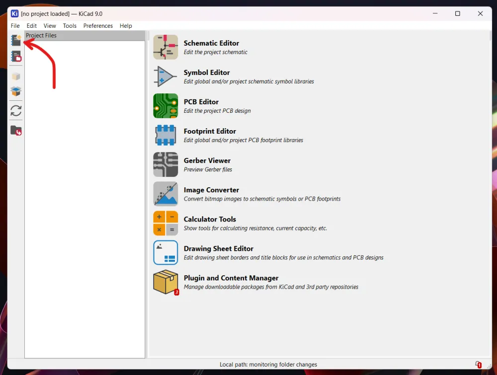
Setting Up a Project
For this guide, we'll be using KiCAD!
Fire up whatever KiCAD version you prefer (I'll be using 9.0.0), and create a new project.
Fleshing Out the Schematic
Start by opening up the Schematic Editor in KiCAD!
The SX1262
In this example, we'll be using the SX1262 radio module by Semtech. Transceiver modules like these are designed to take in a digital signal (in this case, by writing packets into registers over SPI), and send it out over the air waves. Properties like frequency, spreading factor, and power are set as configuration options in software.
To get started, using the Place Symbol tool, place an SX1262 module into your schematic. You may also place down an RP2040 microcontroller.
A lot of concepts from this guide can be transferred over to other microcontrollers like the SAMD21, ATTiny, and others.
Next, we'll put each pin on a local label. In general, use local labels unless you need global labels! We'll also add our decoupling capacitors and power regulation components.
Decoupling capacitors, as the name suggests, decouple the input voltage to the module. For example, if there's a noisy component elsewhere on the board, strong decoupling capacitors will help smooth this ripple out.
The SX1262 has two options for internal power: linear regulator and a switching regulator. We opt for the switching regulator as it's a lot more efficient. However, since they're noisy, we'll need to pay more attention to the PCB routing.
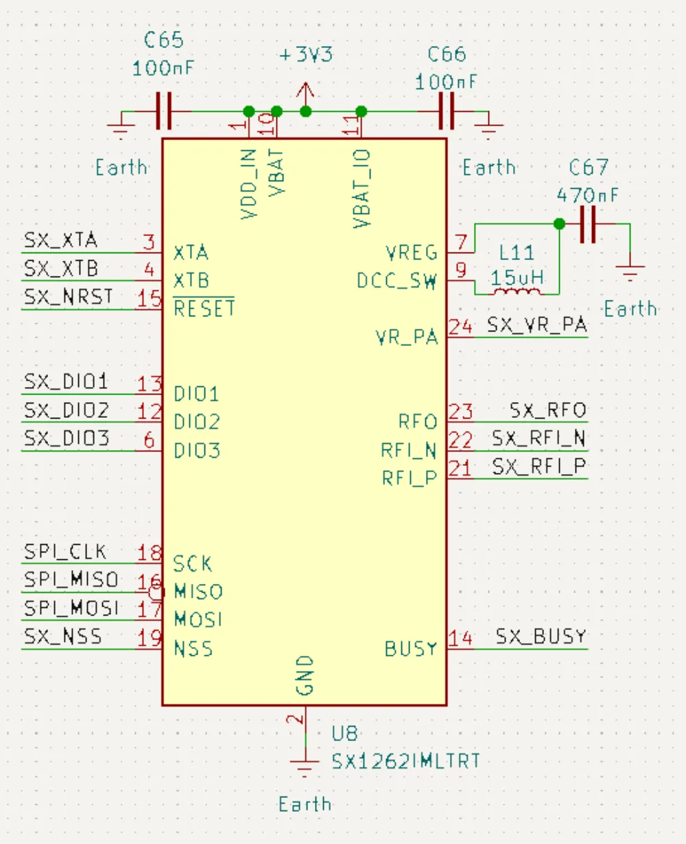
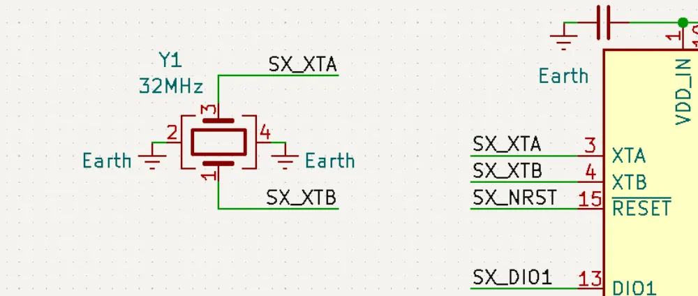
Next, we need to give the module a crystal. It has built-in configurable loading capacitors, so all we need is a direct connection to the chip. The module expects a clean 32MHz signal. I use the Crystal_GND24 symbol
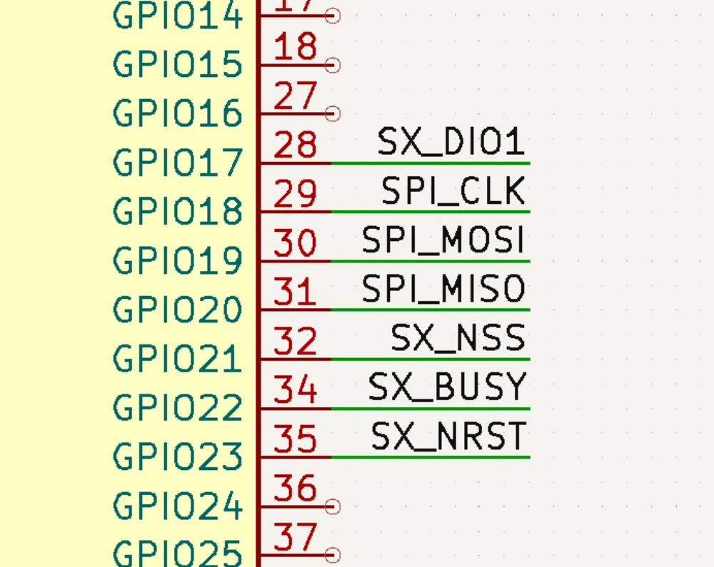
Time to connect it to the RP2040! This module uses SPI, which luckily we broke out to local labels! Here's how I connect them:
SCK -> GPIO18
MOSI -> GPIO19
MISO -> GPIO20
SX_NSS (chip select) -> GPIO21
The SX1262 has 3 configurable GPIO pins. DIO1 defaults to TX/RX control, which is what we're using it for here. There's also some additional digital pins to hook up:
DIO1 (lets us select TX or RX) -> GPIO17
BUSY -> GPIO22
NRST -> GPIO23
Matching and Filtering
It's time to deal with the frontend between the SX1262 and the antenna!
Theory
if you want to skip this, go here.
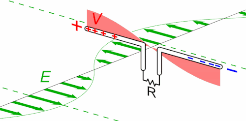
Balun
You may have noticed that the RF inputs are differential. As our antenna is single-ended, we need a balun (literally balanced-unbalanced) to convert RFIP/RFIN to a single-ended signal!
Here's what a typical balun circuit looks like:
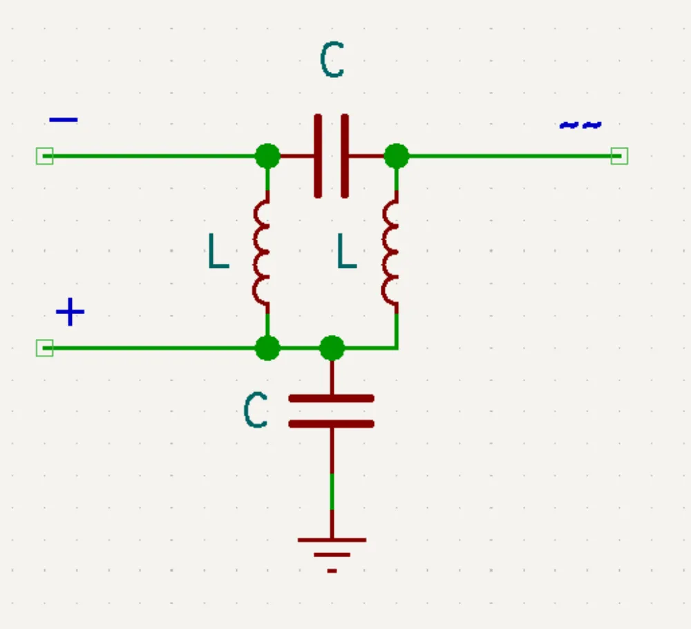
This lets us directly connect the two differential pins of the SX1262 to an antenna frontend!
Impedance Matching
We also need impedance-matching. Here's my attempt to explain this best as possible :sob:
Impedance:
Essentially, impedance is defined as opposition to an AC signal at a specific frequency. Impedance is defined as a complex number composed of two parts: real resistance + imaginary reactance.
Resistance:
This is just the opposition to current flow caused by resistors. This also means resistance introduced by PCB traces and resistance of passive components.
Reactance:
Reactance is the part of impedance that comes from reactive components like inductors and capacitors. It describes how these components resist changes to AC current flow. Inductive reactance increases w.r.t frequency, and capacitive reactance decreases with frequency.
The goal of impedance matching is to keep the impedance of the source, load, and the characteristic impedance of the feedline are all equal. This minimizes reflections and power loss. On a PCB, this often means designing traces and selecting component values to match a target impedance, which we often use 50 ohms.
Filtering
The last step of this process is filtering. This weeds out unwanted harmonics and other spurious emissions.
A sine wave is mathematically the perfect waveform. It contains just one fundamental frequency. However, since ideal sine waves are impossible in real life, every signal has harmonics. These harmonics occur at each whole-number multiples of a fundamental frequency. Here's a nice visualization!
If we neglected these harmonics and just hooked up the output (transmit node) of the SX1262 through matching to the antenna, it will not only emit the desired signal at the desired frequency, but also the signal at undesired harmonics. Hence, we use a low-pass filter. Since harmonics only occur at frequencies higher than the fundamental frequency, we can effectively chop off frequencies above our desired frequency. This can be achieved with a low-pass filter! The drawback is it will introduce some amount of signal loss, even at the desired frequency.
Filters like a low-pass filter are defined by the cutoff frequency, which is the frequency at which the filter starts attenuating. Similarly, band-pass filters (which attenuate frequencies both above and below the desired frequency) are defined by a passband. Since we just need to reject higher frequencies, we can just use a low-pass filter. The simplest version of this would be either an RC (resistor-capacitor) filter, or an LC (inductor-capacitor) filter. LC filters achieve much sharper rolloff!
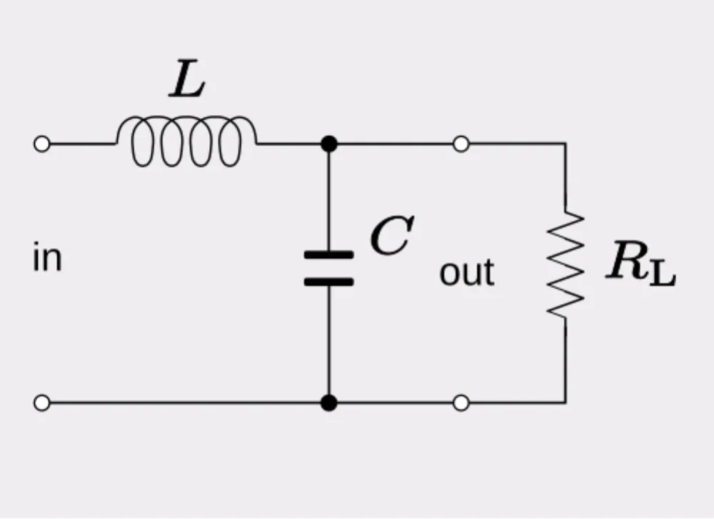
Passive filters like these are also defined by the order. The above image is a first-order filter. As you add more orders, you'll get a better (flatter passband and sharper rolloff) transfer function!
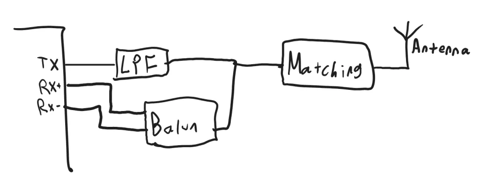
In summary, our frontend should look something like this:
Applying these Concepts
Now here's the fun part: there's a part that does almost all of this for us! The 0900FM15D0039 is an IPD (integrated passive device) by Johanson which contains the balun and filtering (868-915MHz, slightly different footprint [check the datasheet for this, some components may be different!])! We still get to do the pi match ourselves though. To switch between TX and RX, we'll also use an RF switch, controlled by DIO2.
Here's the final frontend schematic. Note the pi network at the end!
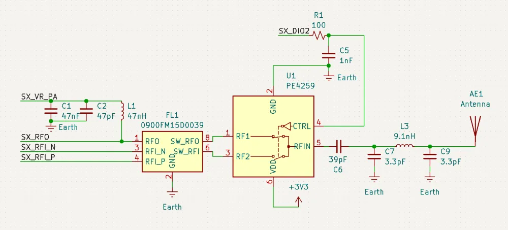
Here's the symbol for the PE4259!
The RP2040
I'm going to speed up this section a bit since many of you may be using different microcontrollers, and tutorials with this microcontroller have been featured several times previously.
Protip: select all pins you want to no-connect, right-click > Pin Helpers > No Connect!
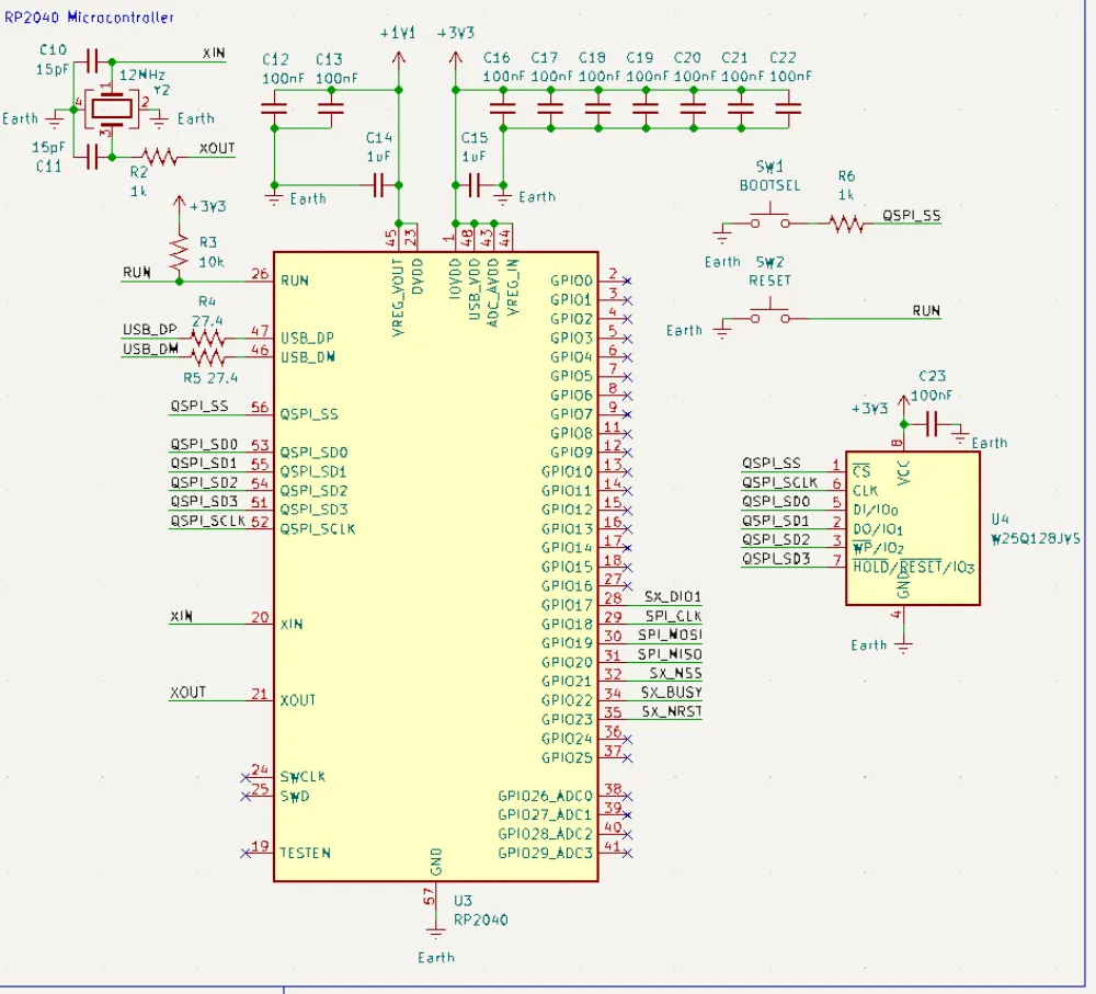
Note that it's good practice to add a small stub of wire in the schematic to make clear that there's a connection. Note the use of decoupling capacitors here again! The values used for the loading capacitors will need to be adjusted per-crystal.
For the USB receptacle, I'll keep it simple for this guide for the sake of brevity, but feel free to add ESD and fuses if desired. I used the AP211K-3.3 as it gives us a lot of current to work with!
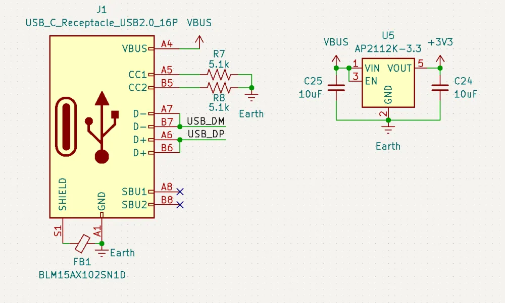
Note the ferrite bead here. The general purpose of this device is to pass DC currents and act as an inductive resistor at higher frequencies. I used the BLM15AX102SN1D, which has low DC resistance, and high inductance at frequencies from 10 MHz to 1 GHz. (this is just the FerriteBead_Small symbol renamed).
When you attach an antenna, there's never a single node. The board ground will act as the other radial. If we simply connected the USB shield to ground, the USB shield itself will resonate, bringing that RF directly into your host device!
Add Footprints!
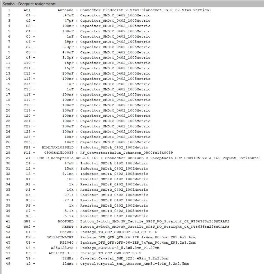
The last step in the schematic, adding footprints.
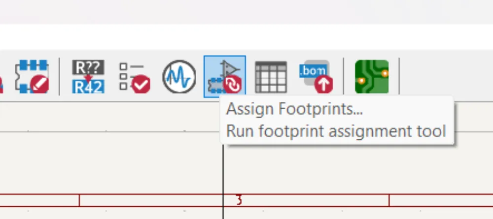
Feel free to use whatever package size you're most comfortable with. The general rule-of-thumb is that smaller and "thinner" packages are more efficient at higher frequencies. I'll be using 0402 components, but feel free to vary. There's several ways to assign footprints in KiCAD, I'll be using the footprint assignment tool here:
Here are my assignments:
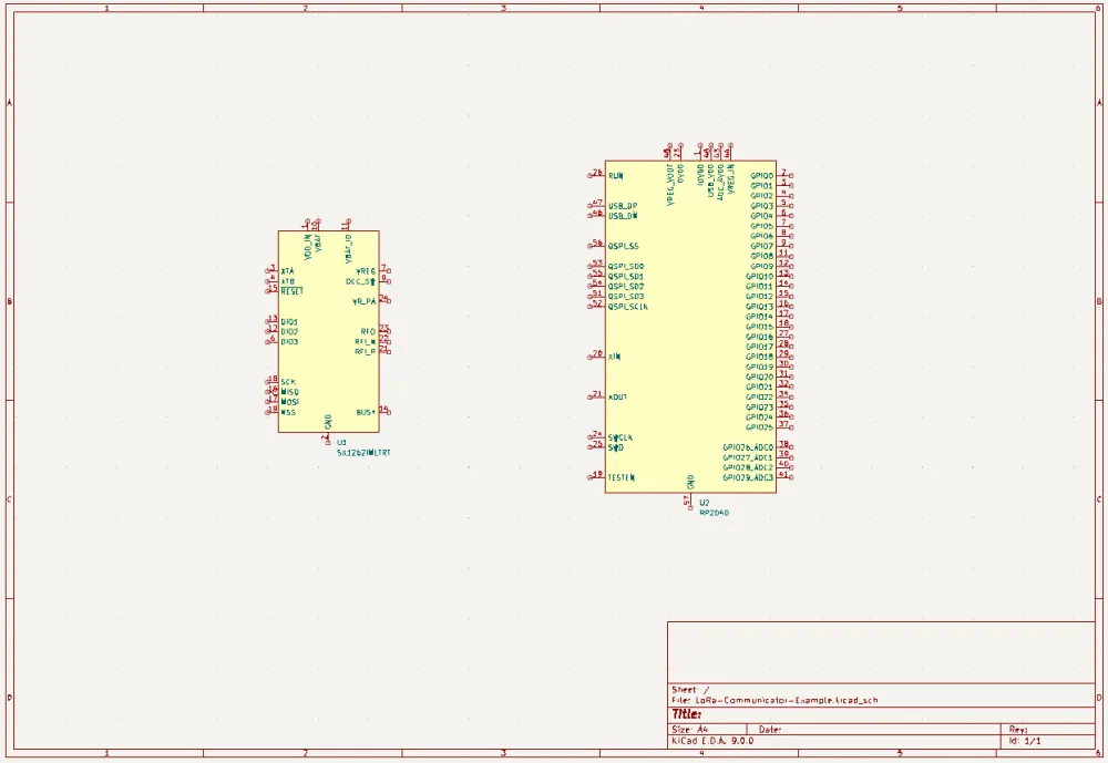
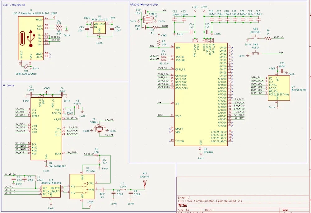
Here's the final schematic design:
PCB Design
Woah, great job getting through the first part! Now we get to (in my opinion) the fun part: the PCB design!
Please consult the Guidelines for Routing RF Traces section when necessary!
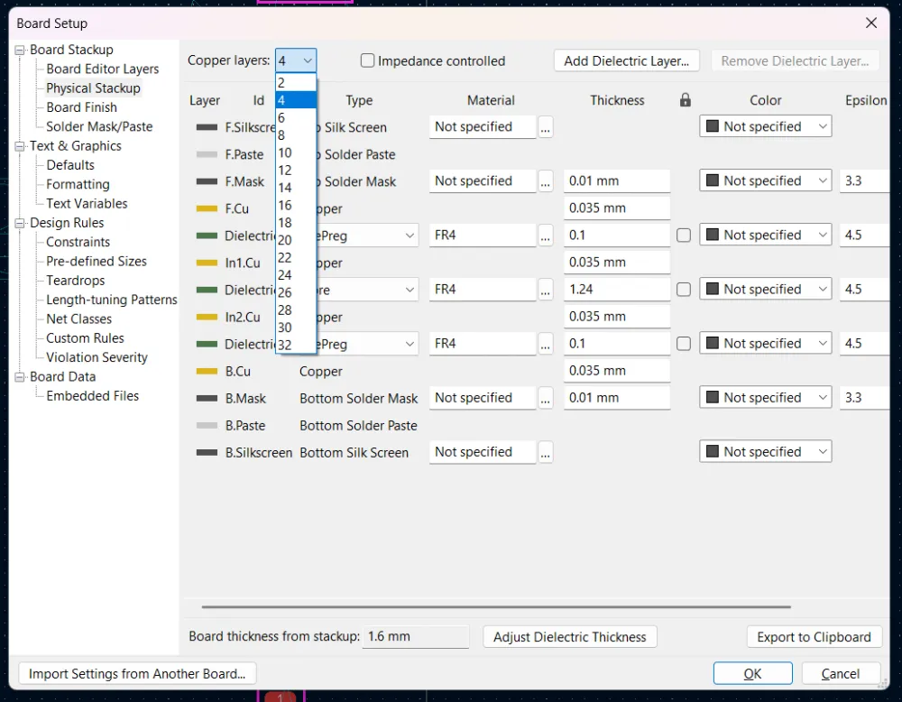
First, head over to Board Setup -> Physical Stackup -> then select 4 copper layers. A dedicated ground reference layer under the RF and other section helps a lot with shielding, and we're left with allowance for a power plane! (note: for more complex boards, power planes should generally be avoided as it's not a good reference).
General Layout
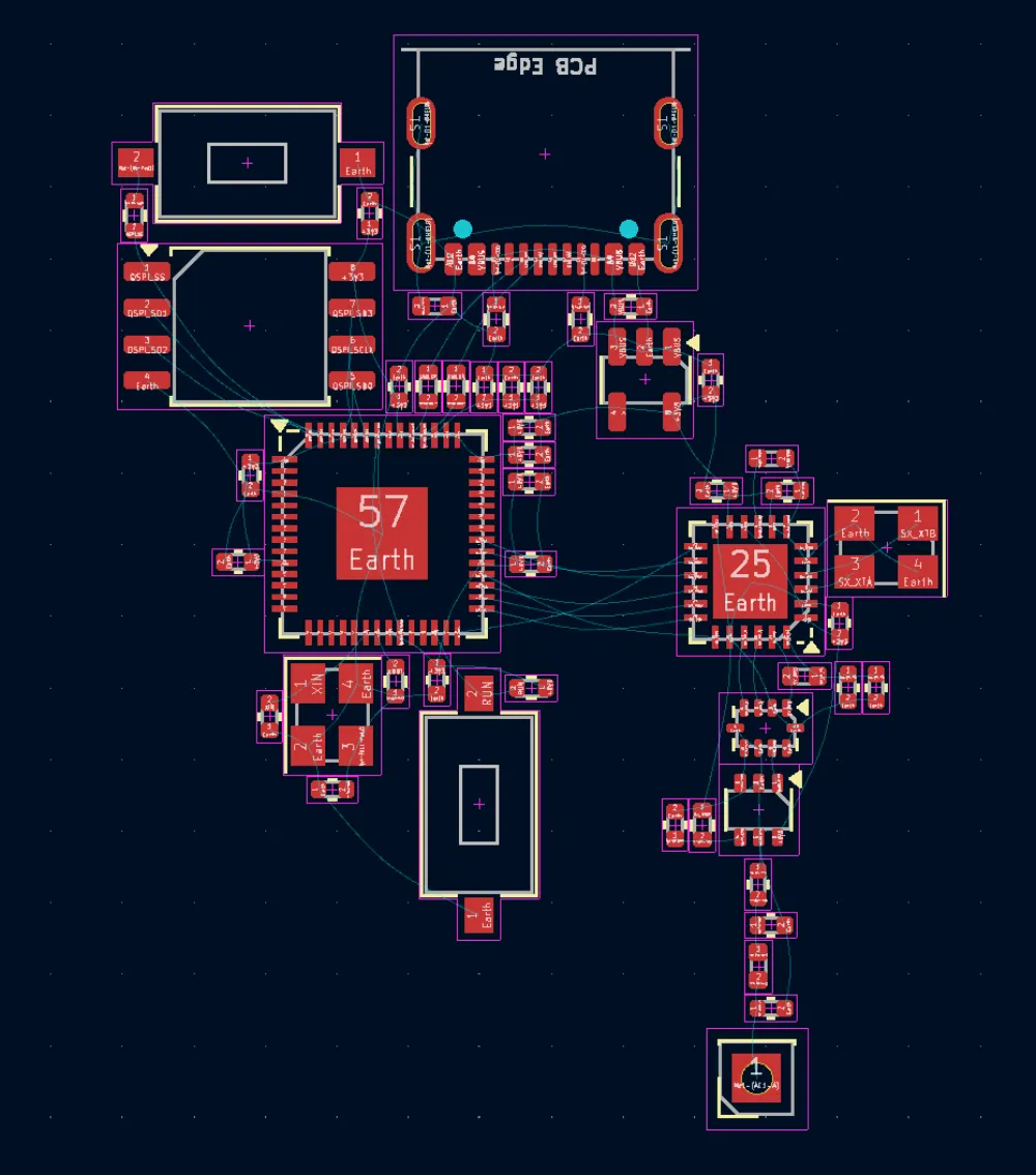
In general, it's good to start with a general layout of parts before routing the traces.
Start by importing the schematic parts into the PCB:
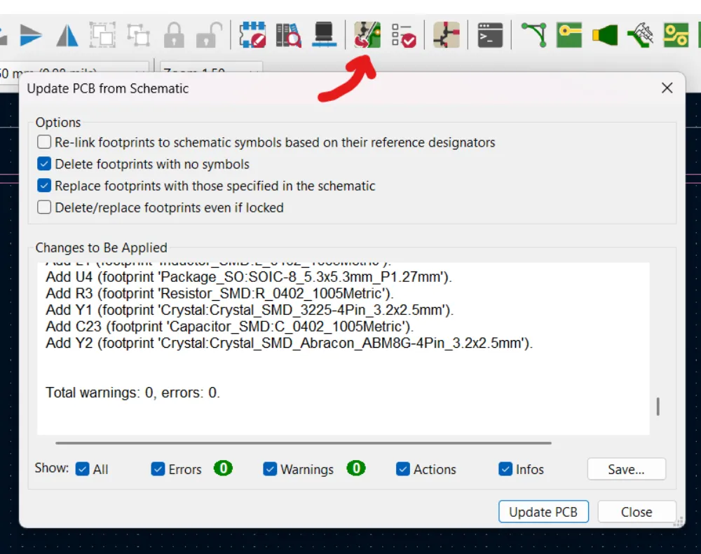
Hit Update PCB to bring in the footprints and netlist.
You have quite a bit of freedom in laying out your PCB. I recommend laying out each section (MCU, Radio, USB) as separate systems, and combining as desired. Remember:
- Keep decoupling capacitors as close to their designated power pins as possible (match it up with the schematic! It makes it a lot easier to come back to it later)
- Keep distances as short as possible, especially for the high-speed flash, and especially the RF
Here's my RF layout:
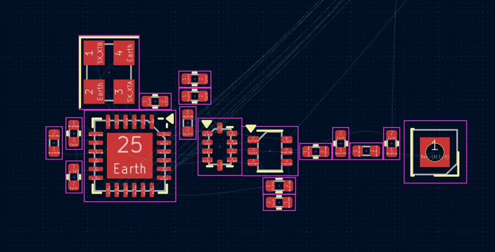
Remember, the inductor by the DCC node is switching high-frequency, so we'll use wide traces to route this. Also note how there is little extraneous distances between components!
Here's how my MCU ended up:
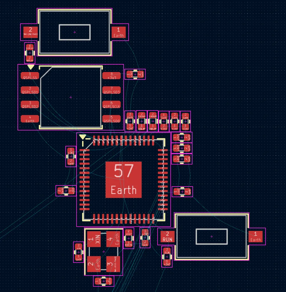
Note the placement of the decoupling capacitors!
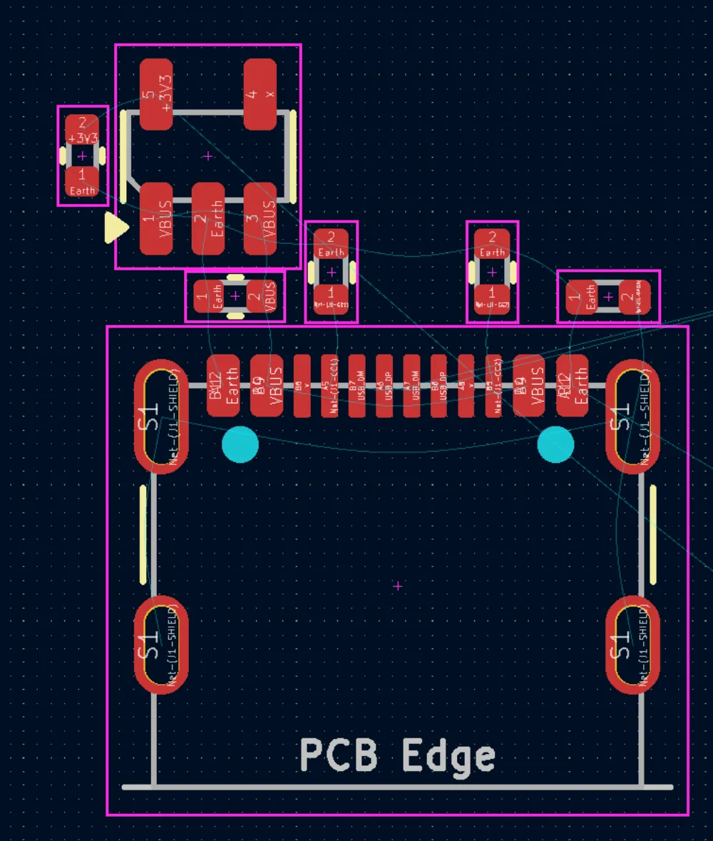
Lastly, here's the USB section layed out:
Here are all of the subsections layed out together! Make sure to give the RF some isolation.
Routing
Once you get your layout drafted, it's time to route! This process can often times change the layout slightly, so be flexible!
The premise is to go from most sensitive -> least sensitive. For this reason, I'll start with the RF, then USB differential pair, then crystals and digital. Have a look at the centralized Guidelines for Routing RF Traces while routing RF!
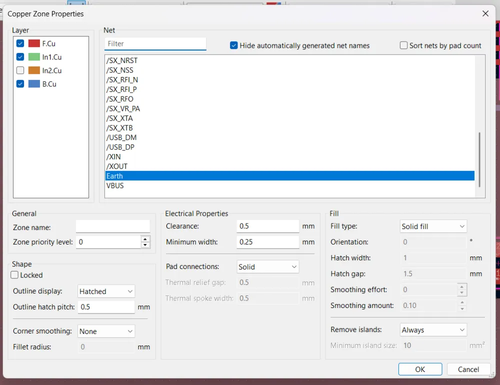
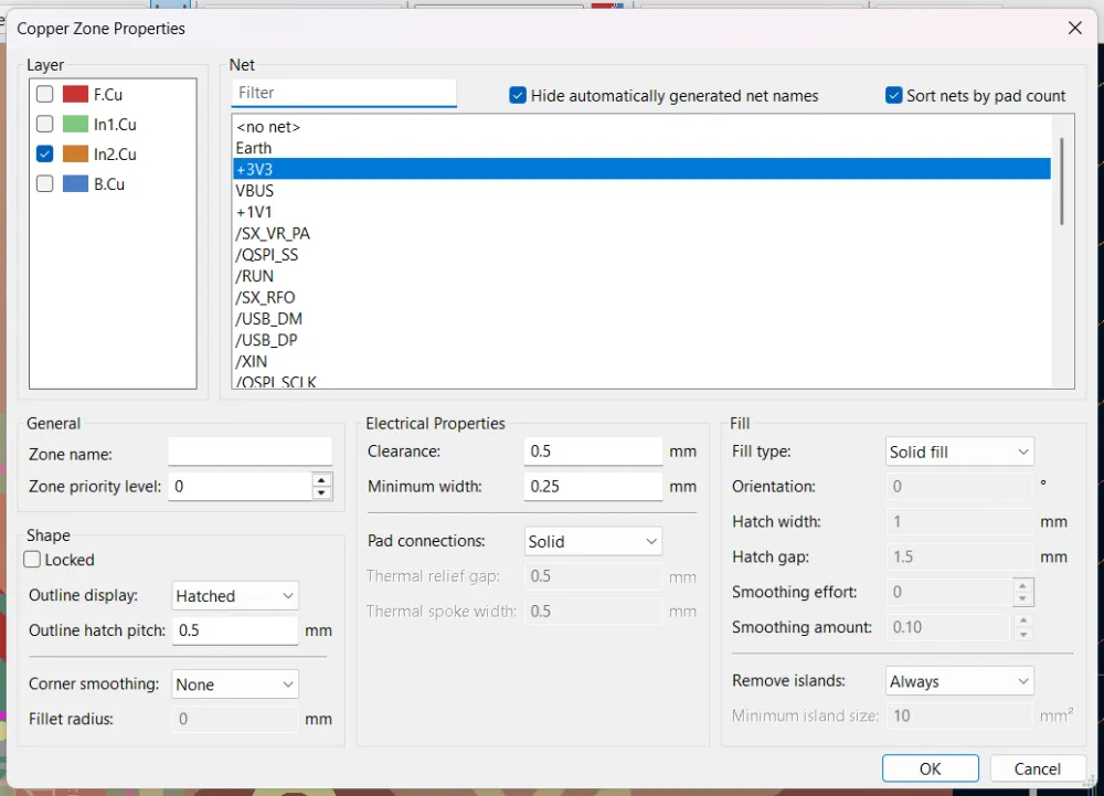
Let's also set up our board outline (rectangle on Edge.Cuts) and zone fill. For zone fill, layers 1,2, and 4 should be filled with ground, and pad connections should be set to solid for better signal integrity. You can always hit B to refill all zones as you're working!
Here's the RF section routed:
Note the use of thick traces on the top for the DC regulator!
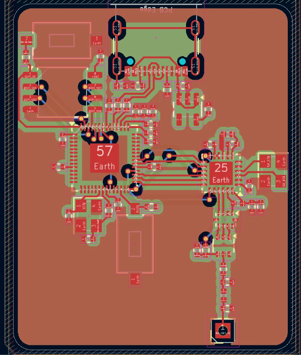
I'll skim over the rest of the routing. The final result before power routing is shown below! Don't worry about power quite yet, as we're gonna use specially-placed ground and power vias to connect!
Delivering Power
We'll do the RF power/ground last, as it's a bit more complex.
First let's add our power plane! For more complex designs you would typically use all ground on inner layers, but it's good enough for us since we don't have a lot of sensitive signals on the back!
Add a new zone on layer 3 (In.2 by default) on the 3.3v net:
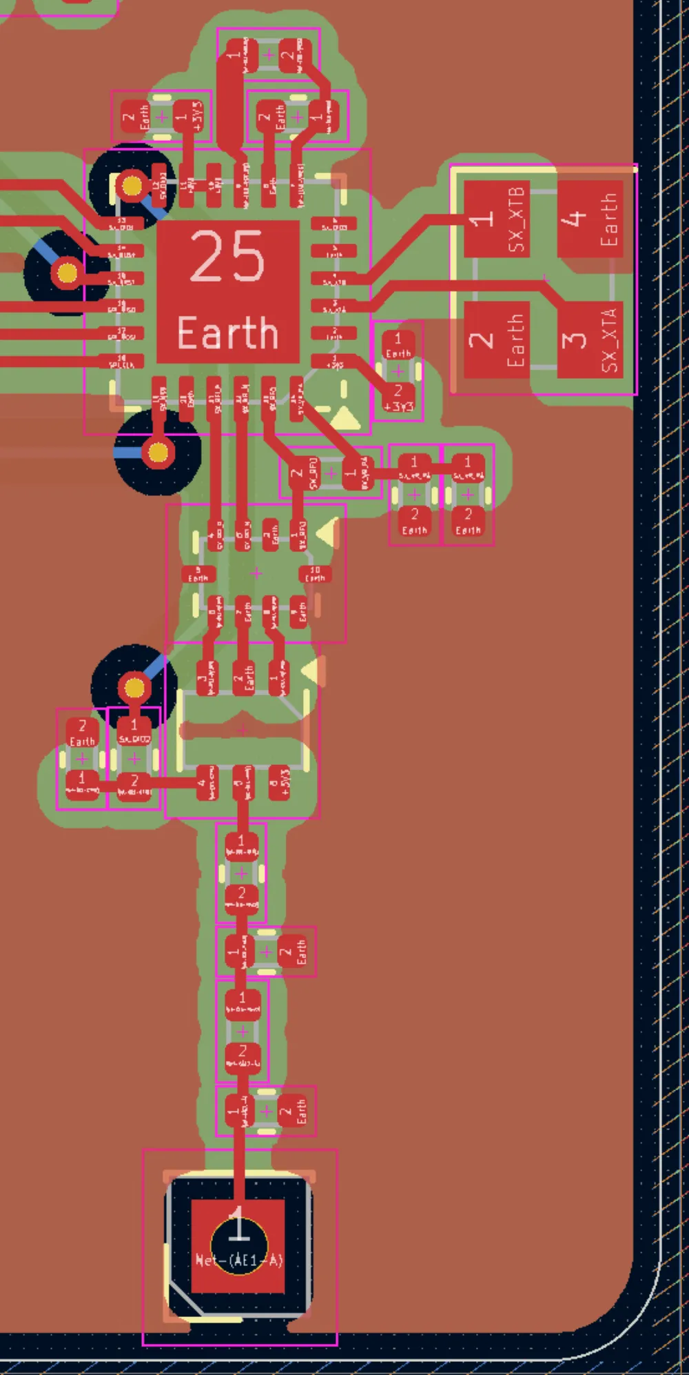
In essence, just add vias as close as possible to the pad. Generally, avoid via-in-pad, as it can create manufacturing problems. I also suggest continuously refilling all zones (B key) to make sure you don't have too many big holes or notches. We do this to ensure all of our return paths are uninterrupted!
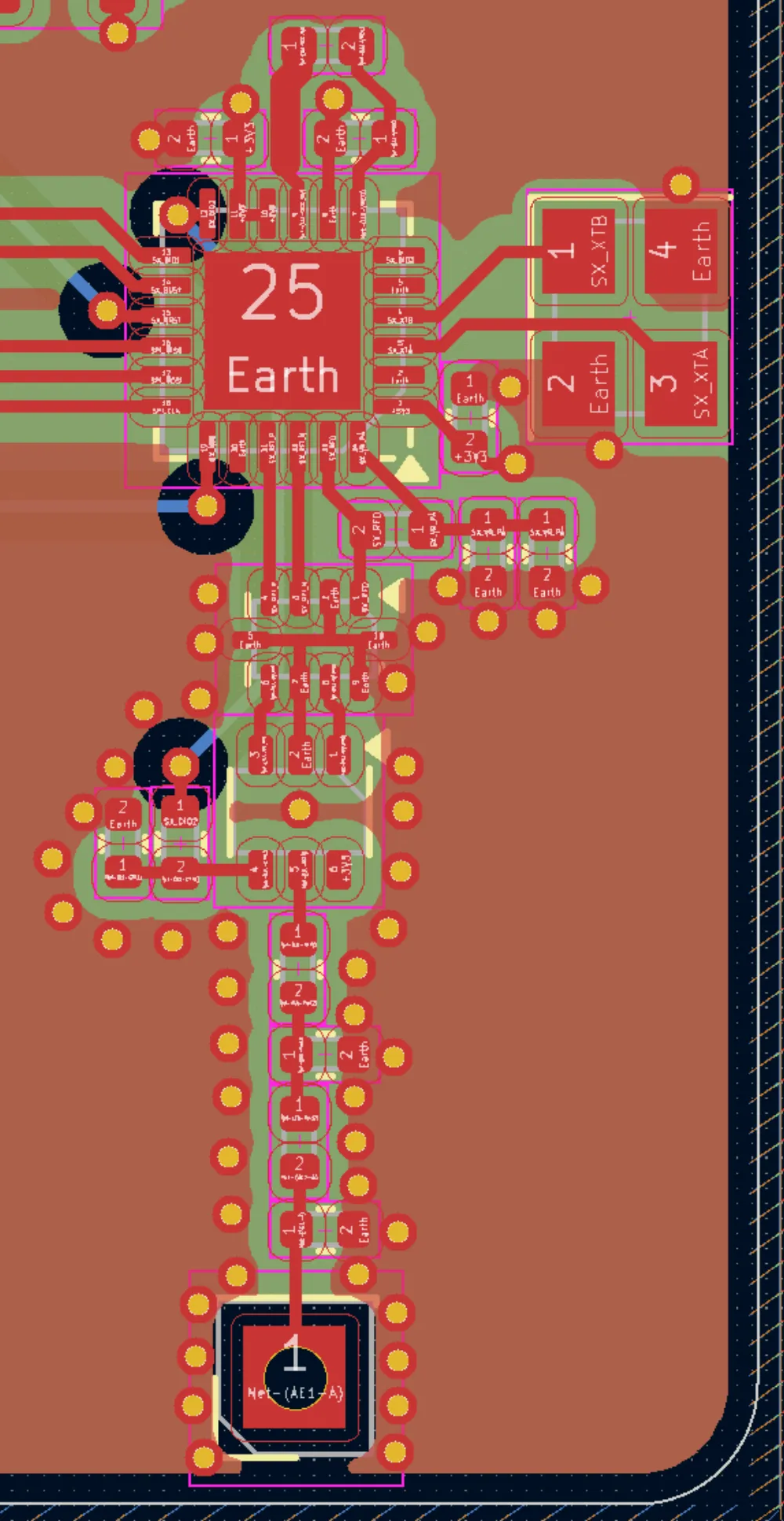
For the RF power, we'll also combine this with via fences. The goal of via fences is to isolate the noise created by the module to it's own section on the ground plane with the use of grounding vias. This also keeps all the grounds equal, eliminating potential grounds. As a general rule of thumb, use 3 ground vias per shunt node!
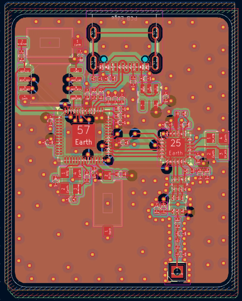
Finally, let's finish via stitching on the rest of our board and fences along the edges (to prevent harmful effects from the skin effect!). Over large, unconnected regions, or flaps, of ground planes, add a via to keep potential grounds away. Then, add a series of closely-packed vias along the edge!
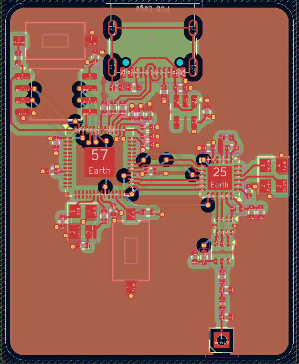
Here's the completed routing:
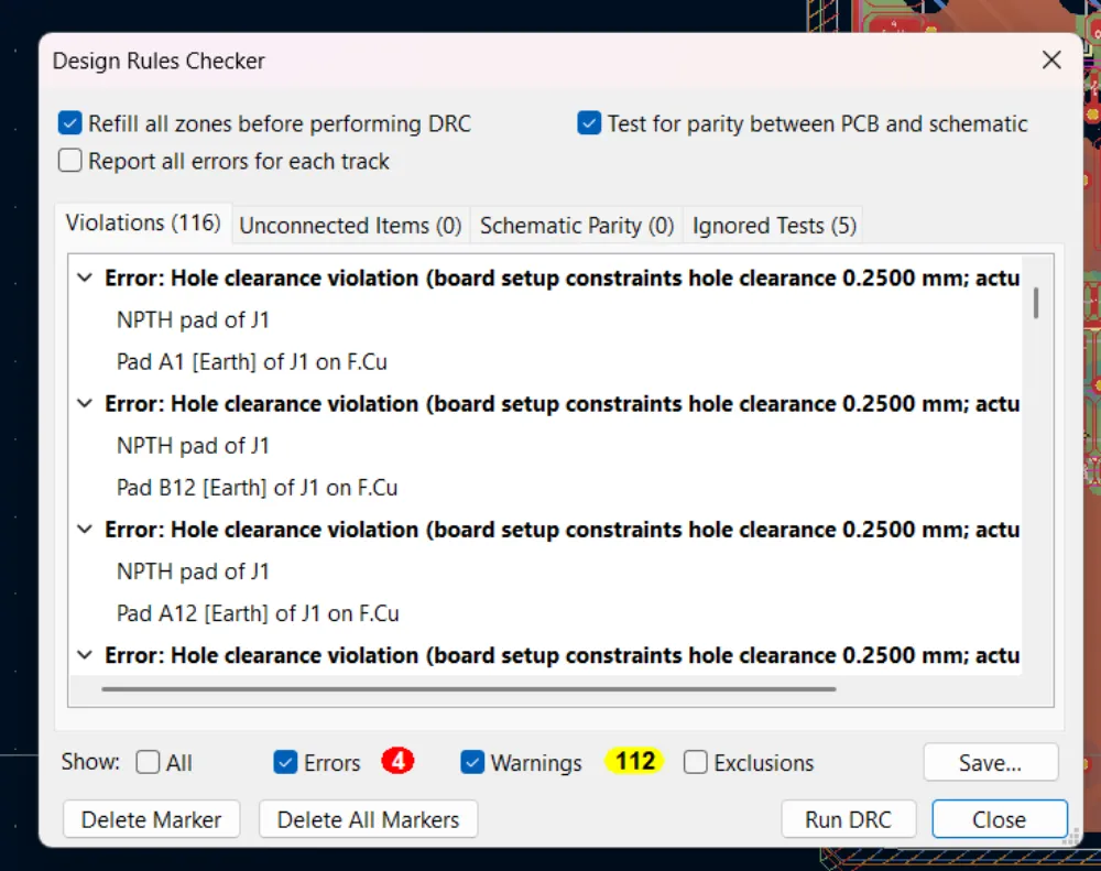
Make sure to check DRC, as we're done routing now! The 4 errors are just from the USB footprint.
Silkscreen and Decor!
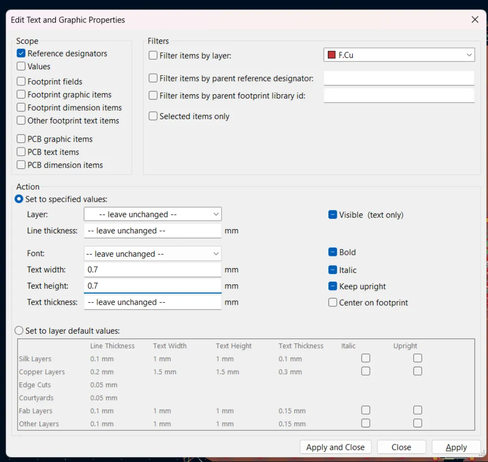
Finally! Before we get into fancy design, let's just straighten out the reference designators.
I recommend going to Edit > Edit Text & Graphics Properties, and check reference designators and change width/height to 0.7mm to make it smaller.
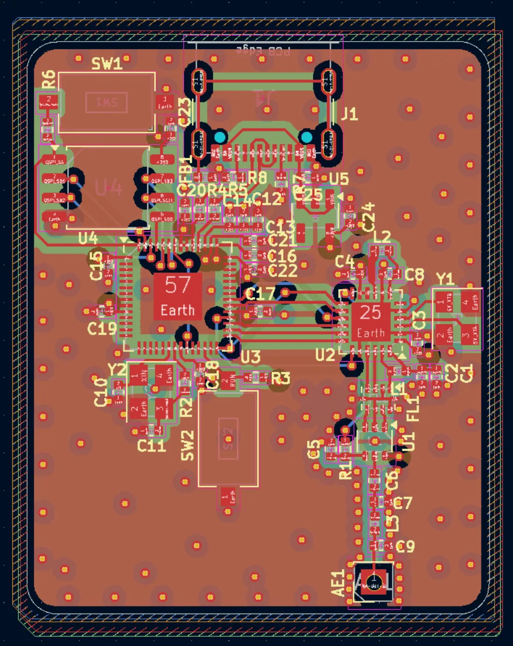
After a few minutes of playing around with reference designators, here's what I got.
Art time! I went for some text and a Hack Club/Blueprint logo, feel free to add your own! You may find that KiCAD's Image Converter tool is great for this, just delete the default reference designators (G***).
And...
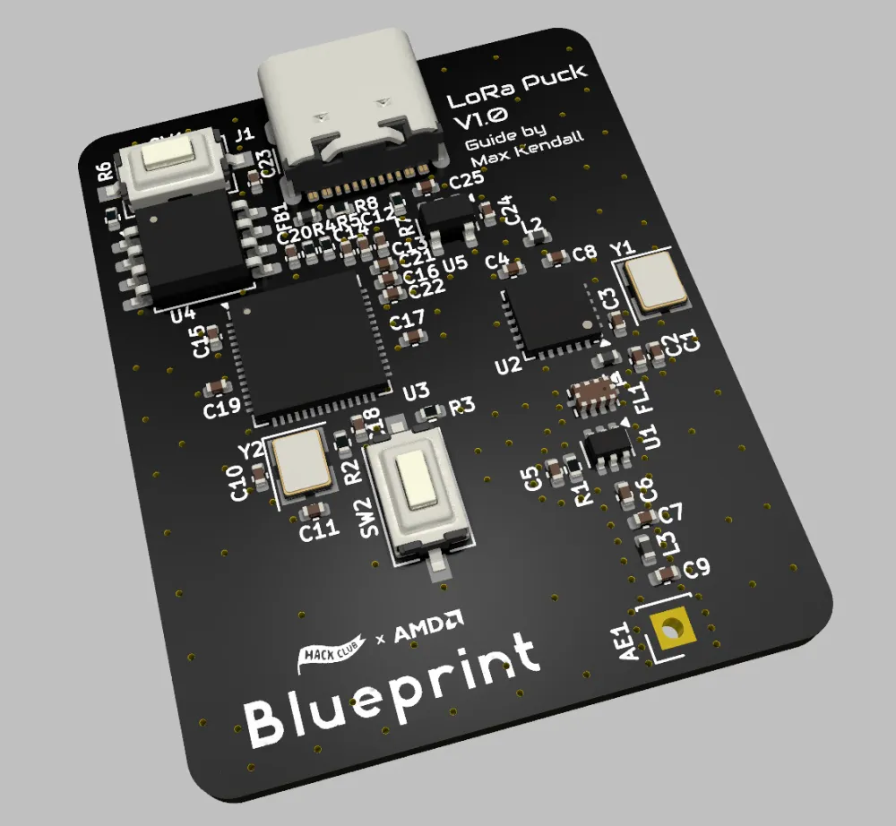
Done!
Guidelines for Routing RF Traces
Since these signals are relatively high frequency (approaching 1GHz), we need to pay very special attention to how we route the traces carrying these signals. Below is an oversimplification of some quite complex rules, but these should provide a general guide to follow.
- Ensure traces are impedance-matched
- Distances are as short as possible
- No right-angles. Use curved or milled bends if needed
- Every trace has a reference. Control the return path with vias. The goal is to keep the return path as short as possible
- Any sensitive signal going through a via should have at least 2 surrounding ground vias to minimize parasitic inductance
Calculating Transmission Lines
KiCAD actually has a built-in calculator tool with all sorts of calculations! We'll be using the transmission line calculator to calculate the properties of our RF traces.
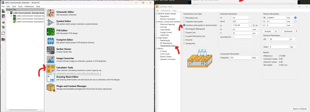
CPWG with Ground is the type of trace we're using. Co-planar just means that there is filled copper surrounding it. With ground just means there's a filled ground plane under the trace.
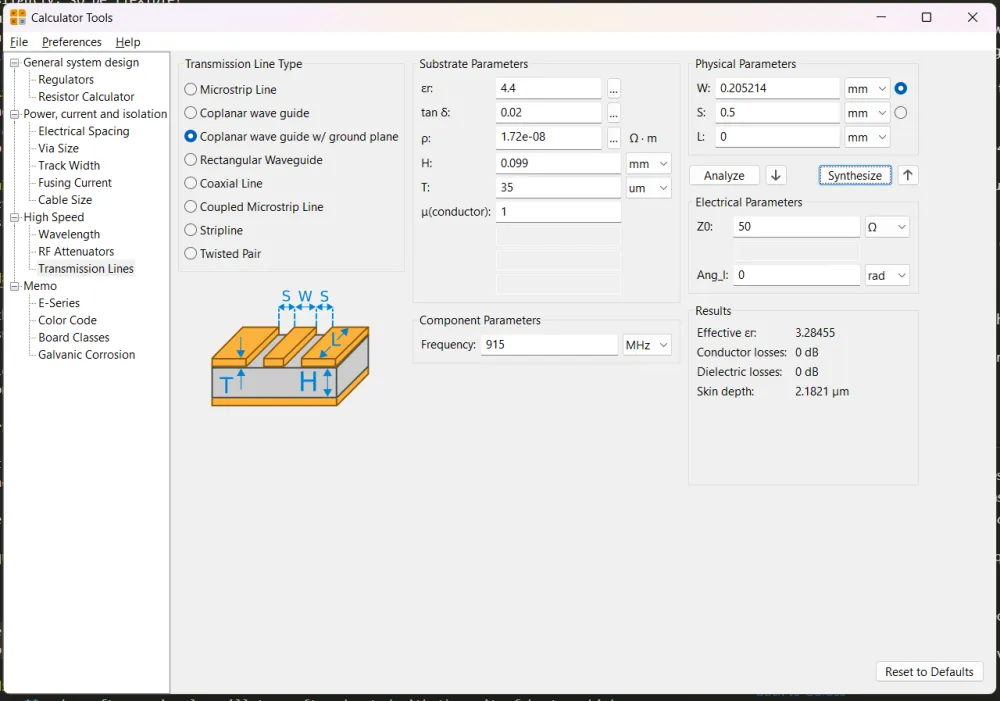
The dielectric constant can be found on the manufacturer's website, but it doesn't have a big effect on the result. I'll use 4.2 as that's JLCPCB's default.
Dielectric loss can be kept at 0.02 as FR-4.
The next setting, DC resistance, is attributed to the type of metal. Since we're using copper, click the 3 dots and select copper.
H is the height of the prepreg. We'll use 0.099, as that's JLCPCB's 3313 stackup setting.
The frequency is 915 MHz!
Finally, for S, we'll use 0.5mm, as that's the KiCAD default for zone fill clearance.
Next, we're targeting 50 ohms, so we can just hit Synthesize! This finallly gives us our trace width to use while routing the RF traces.
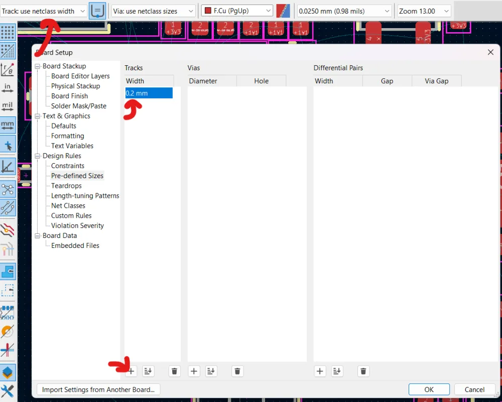
Let's add this to out KiCAD trace widths:
Appendix
frequency - how often a signal oscillates, often denoted with the unit of hertz, which measures oscillations per second. Each radio transmission happens on a specific frequency, and as long as two signals are on different frequencies, they wont interfere. *this is oversimplified. for additional info, look online!
ISM Band - a license-free section of frequencies for "Industrial, Scientific, and Medical". We'll be using the one between 902-928 MHz.
differential - data values are determined by the difference of two nodes.
single-ended - opposite of differential, value is interpreted absolutely as opposed to relatively.